Table of Contents
Advertisement
Quick Links
Advertisement
Table of Contents

Related Manuals for Alpha Data ADA-R9100


Summary of Contents for Alpha Data ADA-R9100
- Page 1 ADA-R9100 User Manual Document Revision: 1.2 10th October 2023...
- Page 2 ADA-R9100 User Manual V1.2 - 10th October 2023 © 2023 Copyright Alpha Data Parallel Systems Ltd. All rights reserved. This publication is protected by Copyright Law, with all rights reserved. No part of this publication may be reproduced, in any shape or form, without prior written consent from Alpha Data Parallel Systems Ltd.
-
Page 3: Table Of Contents
ADA-R9100 User Manual V1.2 - 10th October 2023 Table Of Contents Product Description ......................... 1 HW Modules ............................. 3 FPGA and SFP/QSFP ........................3 CPU board ............................. 3 Redundant PSU (RPSU) ........................ 4 HW Interfaces ........................... 5 Installing the Chassis ........................7 Operating System and Pre-installed SW .................. - Page 4 AD01474 pinout ..........................35 Table 12 SFP delays ............................56 Table 13 QSFP delays ............................ 60 List of Figures Figure 1 ADA-R9100 Appliance ........................1 Figure 2 R9100 HW modules ........................... 3 Figure 3 Interfaces ............................5 Figure 4 Chassis Elements ..........................7 Figure 5 Securing the mount support to the rack .....................
- Page 5 ADA-R9100 User Manual V1.2 - 10th October 2023...
- Page 6 ADA-R9100 User Manual V1.2 - 10th October 2023 Page Intentionally left blank...
-
Page 7: Product Description
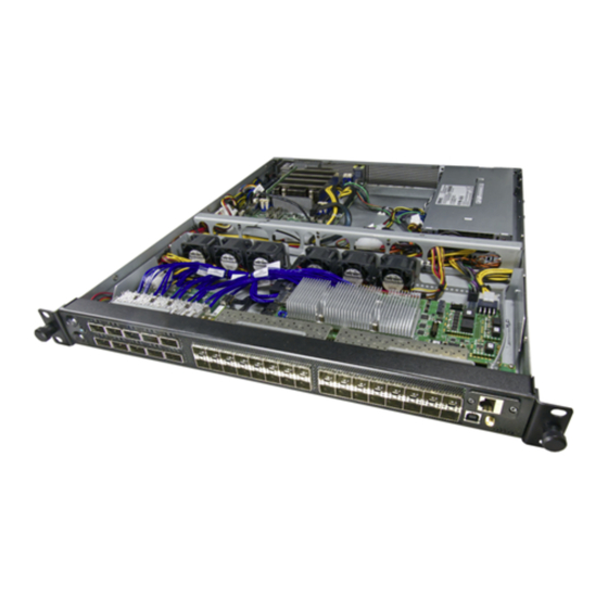
V1.2 - 10th October 2023 1 Product Description The ADA-R9100 is a 1U 19" Rack Mount appliance based around the AMD Ultrascale+ VU2P Ultra Low Latency FPGA. This appliance is designed to provide the lowest latency access to the highest number of ultra-low latency GTF transceivers that are the unique feature of the VU2P device. - Page 8 ADA-R9100 User Manual V1.2 - 10th October 2023 Description Measure Total Dy 540 mm Total Dx 484 mm Total Dz 44 mm Weight 11.28 kg PSU Rating 500W Table 1 : Mechanical Dimensions (Without Rails) Page 2 Product Description ad-sp-r9100_v1_2.pdf...
-
Page 9: Hw Modules
The AD01474 is fitted with an AMD Virtex UltraScale+ VU2P, an ultra-low latency FPGA device. The low-latency lanes are driven by the Xilinx GTF transceivers. The ADA-R9100 has been tested at both 10.3125Gbps and 25.78125Gbps for each low latency lane. -
Page 10: Redundant Psu (Rpsu)
ADA-R9100 User Manual V1.2 - 10th October 2023 2.3 Redundant PSU (RPSU) The system is fitted with a 500W 1+1 redundant power supply (ATX compliant), compatible with CPU boards with 24P connectors. The RSPU is PMBus/SMBUS 1.2 compliant. To operate the RPSU remotely (query state, switch ON/OFF, etc..), see... -
Page 11: Hw Interfaces
ADA-R9100 User Manual V1.2 - 10th October 2023 3 HW Interfaces Figure 3 : Interfaces Front Panel PWR: Power ON/OFF button/indicator. This is a momentary action pushbutton with LED indication. The two independent processing systems (ROMED4ID-2T and AD01474) remain on standby until the button is pressed. - Page 12 ADA-R9100 User Manual V1.2 - 10th October 2023 RST: ROMED4ID-2T’s reset. This is a momentary action pushbutton. It performs a system reset when pressed. QSFP28: Ethernet/Optical connections. There are 5 cages per row and 4 lanes per cage (x40 channels).
-
Page 13: Installing The Chassis
ADA-R9100 User Manual V1.2 - 10th October 2023 4 Installing the Chassis Figure 4 : Chassis Elements Item Description Chassis Base Top Cover Mounting Tray Rack Adjustable Rail Rack Adjustable Hook Bracket M2.5x6 CSK POSI Black M3 KEPS Hex Nut... -
Page 14: Figure 5 Securing The Mount Support To The Rack
ADA-R9100 User Manual V1.2 - 10th October 2023 Figure 5 : Securing the mount support to the rack Now, fit the mounting rail (4), but not too tight (allow some horizontal movement) and slide it all the way back for maximum extension, then slide the unit in the rack until solidly supported by the previously installed rear brackets (5). -
Page 15: Operating System And Pre-Installed Sw
ADA-R9100 User Manual V1.2 - 10th October 2023 5 Operating System and Pre-installed SW The R9100 comes with Ubuntu 18.04.6 LTS preinstalled. It is configured with a graphical desktop and will automatically boot into it when operated locally. SSH is enabled for remote access too. -
Page 16: Powering The System Up
ADA-R9100 User Manual V1.2 - 10th October 2023 6 Powering the System Up The R9100 is equipped with a 1+1 redundant power supply unit (RSPU), and as such both redundant modules need to be sourced for a reliable 24/7 server operation. For best performance, plug both modules into the power... -
Page 17: Full-Power Operation
ADA-R9100 User Manual V1.2 - 10th October 2023 6.2 Full-power operation The system will enter the full-power mode only after the power ON/OFF button of the R9100 has been pressed while in standby mode (see Section 3, item 1). The system will boot into the preinstalled Ubuntu OS and show the login screen with the default user. -
Page 18: Feature Description
ADA-R9100 User Manual V1.2 - 10th October 2023 7 Feature Description 7.1 IPMI PCIe/I2C There is an internal IPMI (PCIe/I2C) connection between the CPU System and the AD01474. It can handle the IPMI commands locally from the CPU system as a local I2C device, or remotely through the IPMI tree by the BMC/CPU Ethernet connections. -
Page 19: Input Clock Reference
ADA-R9100 User Manual V1.2 - 10th October 2023 Note: You will need to deactivate flow control in Minicom by: Ctr-A Z --> Configure Minicom(O) --> Serial port setup --> HW flow control --> OFF --> SW flow control --> OFF Alternatively, run minicom -s to change parameters or modify the file minirc.dlf with the following lines to... -
Page 20: Leds
7.5 LEDs 7.5.1 System LEDs There are 9 system LEDs on the ADA-R9100, 6 of which are general purpose and whose meaning can be defined by the user. The other 3 have fixed functions described below: Figure 8 : Front Panel LEDs Comp. -
Page 21: Sfp+ Cages Leds
ADA-R9100 User Manual V1.2 - 10th October 2023 7.5.2 SFP+ cages LEDs There are 2 LEDs per SFP+ cage, arranged in pairs of 2 together (for the top and bottom cages). The two on the right-hand side are the "module present" signal of each cage, whereas the two on the left are the "link up"(or user definable) of either one. -
Page 22: Qsfp/Sfp
The reprogrammable clocks from the LMK61E2 are reconfigurable from the USB front/back interface by using Alpha Data’s avr2util utility. This allows the user to configure almost any arbitrary clock frequency during application run time for the SFP/QSFP reference clock. The maximum clock frequency for the LMK61E2 is 900MHz. -
Page 23: Figure 12 Clock Topology
ADA-R9100 User Manual V1.2 - 10th October 2023 SFP side of FPGA FPGA GPIO SI5324_1V8_SDA SI5324_1V8_SCL SI5324_0_OUT_1 (MGTREFCLK0) NC (MGTREFCLK1) MEZ_CLK (MGTREFCLK0) NC (MGTREFCLK1) I2C + Si5324_0 CLKOUT1 CNTRL Crystal SI5324_0_OUT_2 (MGTREFCLK0) (2.5V VCC) XA/XB CLKOUT2 114.285MHz SI5324_0_IN1 NC (MGTREFCLK1) -
Page 24: Lmk61E2
ADA-R9100 User Manual V1.2 - 10th October 2023 7.7.1 LMK61E2 The ADM-R9100 uses the LMK61E2 for arbitrary clock frequency synthesis. For complete technical details, please reference the datasheet: https://www.ti.com/lit/ds/symlink/lmk61e2.pdf The ADM-R9100 uses two LMK61E2 devices in the clock architecture. These can be accessed through either the USB or PCIe link using the AVR2UTIL application. -
Page 25: Si5324
ADA-R9100 User Manual V1.2 - 10th October 2023 7.7.3 Si5324 Please note that some net names in the design refer to the SI5324 as an SI5328. These devices are footprint and functionally compatible. The SI5324E-C-GM was chosen at the time of production due to availability concerns and is the part fitted on every board. -
Page 26: Configuration
The Alpha Data System Monitor is also capable of reconfiguring the flash memory and reprograming the FPGA. This provides a useful failsafe mechanism to re-program the FPGA even if it drops off the PCIe bus. The system monitor can be accessed with avr2util over USB at the front panel and rear edge. -
Page 27: Configuration Via Jtag
ADA-R9100 User Manual V1.2 - 10th October 2023 Program with Vivado Hardware Manager with these settings (see xapp1233): • SPI part: mt25qu01g-spi-x1_x2_x4 • State of non-config mem I/O pins: Pull-none 7.8.2 Configuration via JTAG A micro-USB AB Cable may be attached to the front panel or rear edge USB port. This permits the FPGA to be reconfigured using the Xilinx Vivado Hardware Manager via the integrated Digilent JTAG converter box. -
Page 28: System Monitoring
(through ROMED4ID-2T's BMC). 8.1 AD01474 System Monitor The ADA-R9100's USB connections described in the previous section can be used to directly access the system monitor system on the AD01474. All voltages, currents, temperatures, and non-volatile clock configuration settings can be accessed using Alpha Data's avr2util software at this interface (preinstalled in the Ubuntu OS). -
Page 29: System Monitor Status Leds
ADA-R9100 User Manual V1.2 - 10th October 2023 8.1.1 System Monitor Status LEDs LEDs D35 (Red) and D34 (Green) indicate the card health status. LEDs Status Green Running and no alarms Green + Red Standby (Powered off) Flashing Green + Flashing Red... - Page 30 ADA-R9100 User Manual V1.2 - 10th October 2023 Voltage VCPU full-power 12V rail LAN_1.2V Ethernet chipset voltage 1 LAN_0.83V Ethernet chipset voltage 1 Temperatures (degrees Celsius) CPU Temp CPU on-die temperature MB Temp Motherboard chipset temperature TR1 Temp AD01474 FPGA on-die temperature...
-
Page 31: Using Vivado Lab To Program The Ad01474
ADA-R9100 User Manual V1.2 - 10th October 2023 9 Using Vivado Lab to program the AD01474 Once the system is powered up and has booted into Ubuntu, the default user credentials must be provided to log into Ubuntu through its GUI. -
Page 32: Figure 16 Opening Hw Manager
ADA-R9100 User Manual V1.2 - 10th October 2023 Figure 16 : Opening HW Manager Click on the 'Open Target' button that appears at the top, then select 'Auto Connect.' The software will scan the JTAG chain for the FPGA and display its programming status upon detection. This occurs because the FPGA is automatically programmed with a default image from Flash during power-up. -
Page 33: Figure 18 Reprogramming The Fpga
ADA-R9100 User Manual V1.2 - 10th October 2023 Figure 18 : Reprogramming the FPGA Note: Example designs are available for this system. You can request them at support@alpha-data.com. Using Vivado Lab to program the AD01474 Page 27 ad-sp-r9100_v1_2.pdf... -
Page 34: Management Interface (Bmc)
ADA-R9100 User Manual V1.2 - 10th October 2023 10 Management interface (BMC) The BMC processor provides the server capabilities to the system addresses, managing the different services and subsystems. The R9100 is configured to get IP adressess for the BMC and the CPU system automatically. In order to gain access to the system, the assigned IP address by your DHCP server is needed. -
Page 35: Remote Connection To Server (Gui)
ADA-R9100 User Manual V1.2 - 10th October 2023 Figure 21 : BMC's administrator login You will be able to browse through the BMC's different options. See the sensors list below: Figure 22 : BMC's sensors list 10.2 Remote connection to server (GUI) Now, let us open the KVM options to remote control the CPU system. -
Page 36: Figure 23 Kvm Remote Control
ADA-R9100 User Manual V1.2 - 10th October 2023 Figure 23 : KVM remote control Next, the login screen of the CPU system (Ubuntu) will be displayed: Figure 24 : Ubuntu through KVM You can operate the system entirely from here, including performing an ACPI shutdown, reboot, etc. Then you... -
Page 37: Figure 25 Accessing System Bios Remotely
This maximises the available power for the user application on the AD01474/75/76 subsystem and ensures the RPSU operating limits. This is after considering component derating curves and ADA-R9100's safety certification, which specifies a maximum operating temperature of 50 degrees Celsius. The CPU's speed SHOULD NOT be increased. -
Page 38: Remote Control And Monitoring Through Console Commands (Ipmi)
ADA-R9100 User Manual V1.2 - 10th October 2023 11 Remote Control and Monitoring through console commands (IPMI) The main monitoring functions are carried out by ROMED4D-2T's BMC, and these can be accessed through the (Figure 22) or queried with console commands. These are referred to as sensors in the BMC. For a... -
Page 39: Get Cpu Temperature
ADA-R9100 User Manual V1.2 - 10th October 2023 Sensor ID : PSU2 Status (0xa8) Entity ID : 10.0 Sensor Type (Discrete): Power Supply States Asserted : Power Supply [Presence detected] Find below the list of RPSU sensors accessible with PMBus through the ROMED4ID-2T (PSUX=[PSU1|PSU2]):... -
Page 40: Set Commands (Ipmi Raw)
ADA-R9100 User Manual V1.2 - 10th October 2023 11.3 SET Commands (IPMI raw) 11.3.1 Set chassis fan array speeds Fan array speeds are set independently for ROMED4ID-2T and AD01474 to handle their cooling, with two arrays of x3 fans each (Figure 2). -
Page 41: Appendix A Complete Ad01474 Pinout
ADA-R9100 User Manual V1.2 - 10th October 2023 Appendix A: Complete AD01474 pinout Front FPGA FPGA Pin Name Signal Name IO Voltage Panel MGTFRXN0_227 FIREFLY_6_RX0_N J3B1 MGTFRXP0_227 FIREFLY_6_RX0_P J3B1 MGTFRXN1_227 FIREFLY_6_RX1_N J3B1 MGTFRXP1_227 FIREFLY_6_RX1_P J3B1 MGTFRXN2_227 FIREFLY_6_RX2_N J3B1 MGTFRXP2_227 FIREFLY_6_RX2_P... - Page 42 ADA-R9100 User Manual V1.2 - 10th October 2023 Front FPGA FPGA Pin Name Signal Name IO Voltage Panel MGTFRXN0_229 FIREFLY_3_RX0_N J3B3 MGTFRXP0_229 FIREFLY_3_RX0_P J3B3 MGTFRXN1_229 FIREFLY_3_RX1_N J3B3 MGTFRXP1_229 FIREFLY_3_RX1_P J3B3 MGTFRXN2_229 FIREFLY_3_RX2_N J3B3 MGTFRXP2_229 FIREFLY_3_RX2_P J3B3 MGTFRXN3_229 FIREFLY_3_RX3_N J3B3 MGTFRXP3_229...
- Page 43 ADA-R9100 User Manual V1.2 - 10th October 2023 Front FPGA FPGA Pin Name Signal Name IO Voltage Panel MGTFRXP1_132 FIREFLY_8_RX1_P J3B5 MGTFRXN2_132 FIREFLY_8_RX2_N J3B5 MGTFRXP2_132 FIREFLY_8_RX2_P J3B5 MGTFRXN3_132 FIREFLY_8_RX3_N J3B5 MGTFRXP3_132 FIREFLY_8_RX3_P J3B5 MGTFTXN0_132 FIREFLY_8_TX0_N J3B5 MGTFTXP0_132 FIREFLY_8_TX0_P J3B5 MGTFTXN1_132...
- Page 44 ADA-R9100 User Manual V1.2 - 10th October 2023 Front FPGA FPGA Pin Name Signal Name IO Voltage Panel MGTFRXN3_230 FIREFLY_4_RX3_N J3T2 MGTFRXP3_230 FIREFLY_4_RX3_P J3T2 MGTFTXN0_230 FIREFLY_4_TX0_N J3T2 MGTFTXP0_230 FIREFLY_4_TX0_P J3T2 MGTFTXN1_230 FIREFLY_4_TX1_N J3T2 MGTFTXP1_230 FIREFLY_4_TX1_P J3T2 MGTFTXN2_230 FIREFLY_4_TX2_N J3T2 MGTFTXP2_230...
- Page 45 ADA-R9100 User Manual V1.2 - 10th October 2023 Front FPGA FPGA Pin Name Signal Name IO Voltage Panel MGTFTXP0_233 FIREFLY_0_TX0_P J3T4 MGTFTXN1_233 FIREFLY_0_TX1_N J3T4 MGTFTXP1_233 FIREFLY_0_TX1_P J3T4 MGTFTXN2_233 FIREFLY_0_TX2_N J3T4 MGTFTXP2_233 FIREFLY_0_TX2_P J3T4 MGTFTXN3_233 FIREFLY_0_TX3_N J3T4 MGTFTXP3_233 FIREFLY_0_TX3_P J3T4 MGTFRXN0_133...
- Page 46 ADA-R9100 User Manual V1.2 - 10th October 2023 Front FPGA FPGA Pin Name Signal Name IO Voltage Panel MGTFRXN2_129 MGT_129_RX2_N J4B12 MGTFRXP2_129 MGT_129_RX2_P J4B12 AB39 MGTFTXN2_129 MGT_129_TX2_N J4B12 AB38 MGTFTXP2_129 MGT_129_TX2_P J4B12 MGTFRXN0_130 MGT_130_RX0_N J4B13 MGTFRXP0_130 MGT_130_RX0_P J4B13 MGTFTXN0_130 MGT_130_TX0_N...
- Page 47 ADA-R9100 User Manual V1.2 - 10th October 2023 Front FPGA FPGA Pin Name Signal Name IO Voltage Panel AT38 MGTFTXP0_126 MGT_126_TX0_P J4B5 AM44 MGTFRXN2_126 MGT_126_RX2_N J4B6 AM43 MGTFRXP2_126 MGT_126_RX2_P J4B6 AP39 MGTFTXN2_126 MGT_126_TX2_N J4B6 AP38 MGTFTXP2_126 MGT_126_TX2_P J4B6 AK44 MGTFRXN0_127...
- Page 48 ADA-R9100 User Manual V1.2 - 10th October 2023 Front FPGA FPGA Pin Name Signal Name IO Voltage Panel MGTFTXN1_130 MGT_130_TX1_N J4T13 MGTFTXP1_130 MGT_130_TX1_P J4T13 MGTFRXN3_130 MGT_130_RX3_N J4T14 MGTFRXP3_130 MGT_130_RX3_P J4T14 MGTFTXN3_130 MGT_130_TX3_N J4T14 MGTFTXP3_130 MGT_130_TX3_P J4T14 MGTFRXN1_131 MGT_131_RX1_N J4T15 MGTFRXP1_131...
- Page 49 ADA-R9100 User Manual V1.2 - 10th October 2023 Front FPGA FPGA Pin Name Signal Name IO Voltage Panel AJ45 MGTFRXP1_127 MGT_127_RX1_P J4T7 AL41 MGTFTXN1_127 MGT_127_TX1_N J4T7 AL40 MGTFTXP1_127 MGT_127_TX1_P J4T7 AG46 MGTFRXN3_127 MGT_127_RX3_N J4T8 AG45 MGTFRXP3_127 MGT_127_RX3_P J4T8 AJ41 MGTFTXN3_127...
- Page 50 ADA-R9100 User Manual V1.2 - 10th October 2023 Front FPGA FPGA Pin Name Signal Name IO Voltage Panel IO_L17P_T2U_N8_AD10P_72 DDR4_A14 IO_L14N_T2L_N3_GC_72 DDR4_A15 IO_L24N_T3U_N11_72 DDR4_A16 IO_L22N_T3U_N7_DBC_AD0N_72 DDR4_A2 IO_T2U_N12_72 DDR4_A3 IO_L22P_T3U_N6_DBC_AD0P_72 DDR4_A4 IO_T3U_N12_72 DDR4_A5 IO_L17N_T2U_N9_AD10N_72 DDR4_A6 IO_L18N_T2U_N11_AD2N_72 DDR4_A7 IO_L20P_T3L_N2_AD1P_72 DDR4_A8 IO_L20N_T3L_N3_AD1N_72 DDR4_A9...
- Page 51 ADA-R9100 User Manual V1.2 - 10th October 2023 Front FPGA FPGA Pin Name Signal Name IO Voltage Panel IO_L1P_T0L_N0_DBC_72 DDR4_DM8 IO_L21P_T3L_N4_AD8P_71 DDR4_DQ0 IO_L21N_T3L_N5_AD8N_71 DDR4_DQ1 IO_L6P_T0U_N10_AD6P_71 DDR4_DQ10 IO_L5P_T0U_N8_AD14P_71 DDR4_DQ11 IO_L2N_T0L_N3_71 DDR4_DQ12 IO_L3P_T0L_N4_AD15P_71 DDR4_DQ13 IO_L2P_T0L_N2_71 DDR4_DQ14 IO_L6N_T0U_N11_AD6N_71 DDR4_DQ15 IO_L18N_T2U_N11_AD2N_71 DDR4_DQ16 IO_L18P_T2U_N10_AD2P_71 DDR4_DQ17...
- Page 52 ADA-R9100 User Manual V1.2 - 10th October 2023 Front FPGA FPGA Pin Name Signal Name IO Voltage Panel IO_L20P_T3L_N2_AD1P_71 DDR4_DQ4 IO_L9P_T1L_N4_AD12P_73 DDR4_DQ40 IO_L8N_T1L_N3_AD5N_73 DDR4_DQ41 IO_L11N_T1U_N9_GC_73 DDR4_DQ42 IO_L11P_T1U_N8_GC_73 DDR4_DQ43 IO_L9N_T1L_N5_AD12N_73 DDR4_DQ44 IO_L8P_T1L_N2_AD5P_73 DDR4_DQ45 IO_L12N_T1U_N11_GC_73 DDR4_DQ46 IO_L12P_T1U_N10_GC_73 DDR4_DQ47 IO_L2P_T0L_N2_73 DDR4_DQ48 IO_L5P_T0U_N8_AD14P_73 DDR4_DQ49...
- Page 53 ADA-R9100 User Manual V1.2 - 10th October 2023 Front FPGA FPGA Pin Name Signal Name IO Voltage Panel IO_L5P_T0U_N8_AD14P_72 DDR4_DQ71 IO_L3N_T0L_N5_AD15N_71 DDR4_DQ8 IO_L5N_T0U_N9_AD14N_71 DDR4_DQ9 IO_L22N_T3U_N7_DBC_AD0N_71 DDR4_DQS0_C IO_L22P_T3U_N6_DBC_AD0P_71 DDR4_DQS0_T IO_L4N_T0U_N7_DBC_AD7N_71 DDR4_DQS1_C IO_L4P_T0U_N6_DBC_AD7P_71 DDR4_DQS1_T IO_L16N_T2U_N7_QBC_AD3N_71 DDR4_DQS2_C IO_L16P_T2U_N6_QBC_AD3P_71 DDR4_DQS2_T IO_L10N_T1U_N7_QBC_AD4N_71 DDR4_DQS3_C IO_L10P_T1U_N6_QBC_AD4P_71 DDR4_DQS3_T...
- Page 54 ADA-R9100 User Manual V1.2 - 10th October 2023 Front FPGA FPGA Pin Name Signal Name IO Voltage Panel MGTREFCLK0N_232 FIREFLY_CLK_0_PIN_N MGT REFCLK MGTREFCLK0P_232 FIREFLY_CLK_0_PIN_P MGT REFCLK AA10 MGTREFCLK0N_229 FIREFLY_CLK_1_PIN_N MGT REFCLK AA11 MGTREFCLK0P_229 FIREFLY_CLK_1_PIN_P MGT REFCLK AG10 MGTREFCLK1N_227 FIREFLY_CLK_2_PIN_N MGT REFCLK...
- Page 55 ADA-R9100 User Manual V1.2 - 10th October 2023 Front FPGA FPGA Pin Name Signal Name IO Voltage Panel MGTYRXN1_225 PCIE_RX2_N MGTYRXP1_225 PCIE_RX2_P MGTYRXN0_225 PCIE_RX3_N MGTYRXP0_225 PCIE_RX3_P MGTYRXN3_224 PCIE_RX4_N MGTYRXP3_224 PCIE_RX4_P MGTYRXN2_224 PCIE_RX5_N MGTYRXP2_224 PCIE_RX5_P MGTYRXN1_224 PCIE_RX6_N MGTYRXP1_224 PCIE_RX6_P MGTYRXN0_224 PCIE_RX7_N...
- Page 56 ADA-R9100 User Manual V1.2 - 10th October 2023 Front FPGA FPGA Pin Name Signal Name IO Voltage Panel BE25 IO_L5N_T0U_N9_AD14N_66 QDR2_0_A13 BE23 IO_L4P_T0U_N6_DBC_AD7P_66 QDR2_0_A14 AU25 IO_L16P_T2U_N6_QBC_AD3P_66 QDR2_0_A15 AU24 IO_L16N_T2U_N7_QBC_AD3N_66 QDR2_0_A16 BA24 IO_L12P_T1U_N10_GC_66 QDR2_0_A17 BB25 IO_L7N_T1L_N1_QBC_AD13N_66 QDR2_0_A18 BB24 IO_L8P_T1L_N2_AD5P_66 QDR2_0_A19 BB21...
- Page 57 ADA-R9100 User Manual V1.2 - 10th October 2023 Front FPGA FPGA Pin Name Signal Name IO Voltage Panel AT17 IO_L18P_T2U_N10_AD2P_D12_65 QDR2_0_D17 IO_L23N_T3U_N9_PERSTN1_I2C AT20 QDR2_0_D2 _SDA_65 AU20 IO_L22P_T3U_N6_DBC_AD0P_D04_65 QDR2_0_D3 AU19 IO_L22N_T3U_N7_DBC_AD0N_D05_65 QDR2_0_D4 AT18 IO_L21N_T3L_N5_AD8N_D07_65 QDR2_0_D5 AR18 IO_L21P_T3L_N4_AD8P_D06_65 QDR2_0_D6 AR17 IO_L20N_T3L_N3_AD1N_D09_65 QDR2_0_D7...
- Page 58 ADA-R9100 User Manual V1.2 - 10th October 2023 Front FPGA FPGA Pin Name Signal Name IO Voltage Panel BC28 IO_T1U_N12_67 QDR2_1_A0 AU31 IO_L21N_T3L_N5_AD8N_67 QDR2_1_A1 AY27 IO_T2U_N12_67 QDR2_1_A10 AT29 IO_L22P_T3U_N6_DBC_AD0P_67 QDR2_1_A11 AW28 IO_L17N_T2U_N9_AD10N_67 QDR2_1_A12 AV28 IO_L17P_T2U_N8_AD10P_67 QDR2_1_A13 AU26 IO_L19P_T3L_N0_DBC_AD9P_67 QDR2_1_A14 AR28...
- Page 59 ADA-R9100 User Manual V1.2 - 10th October 2023 Front FPGA FPGA Pin Name Signal Name IO Voltage Panel BC32 IO_L5P_T0U_N8_AD14P_68 QDR2_1_D16 BD33 IO_L5N_T0U_N9_AD14N_68 QDR2_1_D17 BF38 IO_L8N_T1L_N3_AD5N_68 QDR2_1_D2 BE38 IO_L8P_T1L_N2_AD5P_68 QDR2_1_D3 BF37 IO_L7N_T1L_N1_QBC_AD13N_68 QDR2_1_D4 BE37 IO_L7P_T1L_N0_QBC_AD13P_68 QDR2_1_D5 BD36 IO_L12N_T1U_N11_GC_68 QDR2_1_D6 BD35...
- Page 60 ADA-R9100 User Manual V1.2 - 10th October 2023 Front FPGA FPGA Pin Name Signal Name IO Voltage Panel IO_L12P_T1U_N10_GC_70 REFCLK200_0_PIN_P AY22 IO_L13N_T2L_N1_GC_QBC_66 REFCLK200_1_PIN_N AW23 IO_L13P_T2L_N0_GC_QBC_66 REFCLK200_1_PIN_P BC27 IO_L11N_T1U_N9_GC_67 REFCLK200_2_PIN_N BB27 IO_L11P_T1U_N8_GC_67 REFCLK200_2_PIN_P IO_L11N_T1U_N9_GC_72 REFCLK200_3_PIN_N IO_L11P_T1U_N8_GC_72 REFCLK200_3_PIN_P AY15 IO_L6N_HDGC_AD6N_88 SI5328_0_CLKIN1_N AW15...
- Page 61 ADA-R9100 User Manual V1.2 - 10th October 2023 Front FPGA FPGA Pin Name Signal Name IO Voltage Panel MGTREFCLK0N_230 SI5328_2_CLKOUT2_PIN_N MGT REFCLK MGTREFCLK0P_230 SI5328_2_CLKOUT2_PIN_P MGT REFCLK BC14 IO_L3P_AD9P_88 SI5328_2_INT_C1B BD14 IO_L3N_AD9N_88 SI5328_2_LOL AP15 IO_L11P_AD1P_88 SI5328_2_RST_L AU14 IO_L8N_HDGC_AD4N_88 SI5328_3_CLKIN1_N AU15 IO_L8P_HDGC_AD4P_88...
-
Page 62: Appendix B Sfp Delays
ADA-R9100 User Manual V1.2 - 10th October 2023 Appendix B: SFP delays Trace Trace FPGA Length FPGA Pin Name Signal Name Delay (ps) (mm) AE45 MGTFRXP1_128 MGT_128_RX1_P AE46 MGTFRXN1_128 MGT_128_RX1_N AH44 MGTFRXN2_127 MGT_127_RX2_N AH43 MGTFRXP2_127 MGT_127_RX2_P AG45 MGTFRXP3_127 MGT_127_RX3_P AG46... - Page 63 ADA-R9100 User Manual V1.2 - 10th October 2023 Trace Trace FPGA Length FPGA Pin Name Signal Name Delay (ps) (mm) AM38 MGTFTXP0_127 MGT_127_TX0_P AM39 MGTFTXN0_127 MGT_127_TX0_N AM44 MGTFRXN2_126 MGT_126_RX2_N AM43 MGTFRXP2_126 MGT_126_RX2_P AN41 MGTFTXN3_126 MGT_126_TX3_N AN40 MGTFTXP3_126 MGT_126_TX3_P AL46 MGTFRXN3_126...
- Page 64 ADA-R9100 User Manual V1.2 - 10th October 2023 Trace Trace FPGA Length FPGA Pin Name Signal Name Delay (ps) (mm) AT43 MGTFRXP2_125 MGT_125_RX2_P AU40 MGTFTXP3_125 MGT_125_TX3_P AU41 MGTFTXN3_125 MGT_125_TX3_N AR45 MGTFRXP3_125 MGT_125_RX3_P AR46 MGTFRXN3_125 MGT_125_RX3_N MGTFTXN0_130 MGT_130_TX0_N MGTFTXP0_130 MGT_130_TX0_P MGTFRXP3_130...
- Page 65 ADA-R9100 User Manual V1.2 - 10th October 2023 Trace Trace FPGA Length FPGA Pin Name Signal Name Delay (ps) (mm) AY44 MGTFRXN2_124 MGT_124_RX2_N AY43 MGTFRXP2_124 MGT_124_RX2_P MGTFTXP0_131 MGT_131_TX0_P MGTFRXN3_131 MGT_131_RX3_N MGTFTXN0_131 MGT_131_TX0_N MGTFRXP3_131 MGT_131_RX3_P MGTFTXP1_131 MGT_131_TX1_P MGTFTXN1_131 MGT_131_TX1_N MGTFRXP0_131 MGT_131_RX0_P...
-
Page 66: Appendix C Qsfp Delays
ADA-R9100 User Manual V1.2 - 10th October 2023 Appendix C: QSFP delays Length FPGA Delay (ps) FPGA Pin Name Signal Name (mm) 1191 MGTFRXP1_232 FIREFLY_1_RX1_P 1192 MGTFRXN1_232 FIREFLY_1_RX1_N 1211 MGTFRXN3_232 FIREFLY_1_RX3_N 1211 MGTFRXP3_232 FIREFLY_1_RX3_P 1213 MGTFRXN0_232 FIREFLY_1_RX0_N 1213 MGTFRXP0_232 FIREFLY_1_RX0_P... - Page 67 ADA-R9100 User Manual V1.2 - 10th October 2023 Length FPGA Delay (ps) FPGA Pin Name Signal Name (mm) 1303 MGTFTXN0_232 FIREFLY_1_TX0_N 1307 MGTFRXN3_233 FIREFLY_0_RX3_N 1307 MGTFRXP3_233 FIREFLY_0_RX3_P 1321 MGTFRXN2_233 FIREFLY_0_RX2_N 1321 MGTFRXP2_233 FIREFLY_0_RX2_P 1335 MGTFTXN0_229 FIREFLY_3_TX0_N 1335 MGTFTXP0_229 FIREFLY_3_TX0_P 1337...
- Page 68 ADA-R9100 User Manual V1.2 - 10th October 2023 Length FPGA Delay (ps) FPGA Pin Name Signal Name (mm) 1417 MGTFRXP0_228 FIREFLY_5_RX0_P 1418 MGTFRXP3_228 FIREFLY_5_RX3_P 1419 MGTFRXN3_228 FIREFLY_5_RX3_N 1438 MGTFTXN1_228 FIREFLY_5_TX1_N 1438 MGTFTXP1_228 FIREFLY_5_TX1_P 1445 MGTFRXN2_228 FIREFLY_5_RX2_N 1445 MGTFRXP2_228 FIREFLY_5_RX2_P 1447...
- Page 69 ADA-R9100 User Manual V1.2 - 10th October 2023 Length FPGA Delay (ps) FPGA Pin Name Signal Name (mm) 1545 MGTFTXP2_227 FIREFLY_6_TX2_P 1566 MGTFTXN1_227 FIREFLY_6_TX1_N 1566 MGTFTXP1_227 FIREFLY_6_TX1_P 1567 MGTFRXN3_226 FIREFLY_7_RX3_N 1567 MGTFRXP3_226 FIREFLY_7_RX3_P 1569 MGTFRXN2_226 FIREFLY_7_RX2_N 1569 MGTFRXP2_226 FIREFLY_7_RX2_P 1570...
- Page 70 ADA-R9100 User Manual V1.2 - 10th October 2023 Length FPGA Delay (ps) FPGA Pin Name Signal Name (mm) 2035 MGTFRXP0_133 FIREFLY_9_RX0_P 2045 MGTFRXN1_133 FIREFLY_9_RX1_N 2045 MGTFRXP1_133 FIREFLY_9_RX1_P 2047 MGTFTXN2_133 FIREFLY_9_TX2_N 2047 MGTFTXP2_133 FIREFLY_9_TX2_P 2049 MGTFTXN1_133 FIREFLY_9_TX1_N 2049 MGTFTXP1_133 FIREFLY_9_TX1_P 2074...
-
Page 71: Appendix D System Sensors And Monitoring
ADA-R9100 User Manual V1.2 - 10th October 2023 Appendix D: System Sensors and Monitoring Access Standby Full Power Device Sensor BMCEth Front Panel USB Front Panel UART CPUEth CPUApp FPGA 3VSB 5VSB VCPU VSOC VCCM ABCD VCCM EFGH VPPM ABCD... -
Page 72: Figure 26 Sensors List With Access Options Based On Power Profiles
ADA-R9100 User Manual V1.2 - 10th October 2023 MFR_POUT_MAX MFR_AMBIENT_MAX PSUPDBDevice Device Sensor IPMI IPMI/USB IPMI/USB AVR IPMI IPMI/USB IPMI/USB AVR ADC00(12V AUXrail) IPMI IPMI/USB IPMI/USB AVR ADC01(12V rail) IPMI IPMI/USB IPMI/USB AVR ADC02(12V current) IPMI IPMI/USB IPMI/USB AVR ADC03(3.3V AUXrail) - Page 73 ADA-R9100 User Manual V1.2 - 10th October 2023 Revision History Date Revision Changed By Nature of Change C. Gutierrez - K. Issued 23/05/23 Roth Added complete FPGA pinout and QSFP/SFP cages C. Gutierrez - K. 05/07/23 connection to the FPGA (QUADs)
Need help?
Do you have a question about the ADA-R9100 and is the answer not in the manual?
Questions and answers