Table of Contents
Advertisement
Quick Links
Advertisement
Table of Contents

Related Manuals for Alpha Data ADM-VPX3-9V2


Summary of Contents for Alpha Data ADM-VPX3-9V2
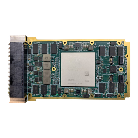
- Page 1 ADM-VPX3-9V2 User Manual Document Revision: 1.2 13th October 2020...
- Page 2 ADM-VPX3-9V2 User Manual © 2020 Copyright Alpha Data Parallel Systems Ltd. All rights reserved. This publication is protected by Copyright Law, with all rights reserved. No part of this publication may be reproduced, in any shape or form, without prior written consent from Alpha Data Parallel Systems Ltd.
-
Page 3: Table Of Contents
ADM-VPX3-9V2 User Manual Table Of Contents Introduction ............................1 Key Features ..........................1 Order Code ............................ 2 Board Information ..........................3 Physical Specifications ........................3 Chassis Requirements ........................4 2.2.1 PCI Express ..........................4 2.2.2 Mechanical Requirements ......................4 2.2.3 Power Requirements ......................... - Page 4 ADM-VPX3-9V2 Product Photo ......................1 Figure 2 ADM-VPX3-9V2 Top View ......................... 3 Figure 3 Thermal Performance ........................5 Figure 4 ADM-VPX3-9V2 VU9P Block Diagram ....................6 Figure 5 ADM-VPX3-9V2 VU13P Block Diagram .................... 7 Figure 6 ADM-VPX3-9V2 with debug board ....................7 Figure 7 Switches ............................
-
Page 5: Introduction
ADM-VPX3-9V2 User Manual 1 Introduction The ADM-VPX3-9V2 is a 3U VPX embedded high-performance reconfigurable computing card intended for high speed switch applications. Featuring 28G transceivers in the Xilinx Virtex UltraScale+ Plus FPGA at all VPX P1 and P2 wafers, and two FireFly sites for rugged optical communications. -
Page 6: Order Code
SLT3-PAY-1F2U-14.2.12 • SLT3-PAY-3F2U-14.2.13 • SLT3-PAY-2U2U-14.2.17 • SLT3-PER-2F-14.3.1 • SLT3-PER-1F-14.3.2 • SLT3-PER-1U-14.3.3 • SLT3-PER-1Q-14.3.4 • SLT3-SWH-6F6U-14.4.1 • SLT3-SWH-8F-14.4.2 • SLT3-SWH-2F24U-14.4.3 • SLT3-SWH-4F-14.4.4 • SLT3-SWH-2F8U-14.4.5 • SLT3-SWH-6F8U-14.4.9 • SLT3-SWH-6F8U-14.4.9 1.2 Order Code See http://www.alpha-data.com/pdfs/adm-vpx3-9v2.pdf for complete ordering options. Page 2 Introduction ad-ug-1377_v1_2.pdf... -
Page 7: Board Information
ADM-VPX3-9V2 User Manual 2 Board Information 2.1 Physical Specifications The ADM-VPX3-9V2 complies with 4HP pitch slot profiles from AV48.1 and AV48.2 respectively Description Measure Total Dy 100 mm PCB Dy 94 mm Total Dx 171 mm PCB Dx 160 mm Total Dz 21.5 mm... -
Page 8: Chassis Requirements
ADM-VPX3-9V2 User Manual 2.2 Chassis Requirements 2.2.1 PCI Express The ADM-VPX3-9V2 is capable of PCIe Gen 3 with up to 16 lanes, using the Xilinx Integrated Block for PCI Express. 2.2.2 Mechanical Requirements A 3U VPX compliant backplane is required for use with this module. -
Page 9: Thermal Performance
If the FPGA core temperature exceeds 105 degrees Celsius, the FPGA design will be cleared to prevent the card from over-heating. The ADM-VPX3-9V2 comes with either a convection or conduction heat sink. The only part of the card monitored for over-temperature shutdown is the FPGA, since it is typically the hottest point on the card. The FPGA die temperature must remain under 100 degrees Celsius. -
Page 10: Functional Description
The ADM-VPX3-9V2 comes with a front access debug board which includes: 8 user LEDs, 4 status LEDs, DIP switch, Xilinx JTAG programing header, micro usb access to system montior, and factory programing headers. -
Page 11: Figure 5 Adm-Vpx3-9V2 Vu13P Block Diagram
Fat Pipe 4GB DDR4-2666 4GB DDR4-2666 72 bits 72 bits Fat Pipe (5x 16 bit BGA) (5x 16 bit BGA) Fat Pipe Figure 5 : ADM-VPX3-9V2 VU13P Block Diagram Figure 6 : ADM-VPX3-9V2 with debug board Functional Description Page 7 ad-ug-1377_v1_2.pdf... -
Page 12: Switches
ADM-VPX3-9V2 User Manual 3.1.1 Switches The ADM-VPX3-9V2 has a quad DIP switch SW1, located on the debug board. The function of each switch in SW1 is detailed below: Figure 7 : Switches Factory Switch Function OFF State ON State Default... -
Page 13: Leds
3.1.2 LEDs There are 12 LEDs on the ADM-VPX3-9V2 debug board, 8 of which are general purpose and whose meaning can be defined by the user. These user LEDs do not have a default value, and could be in any state when the FPGA is unconfigured, or these pins are unconstrained (i.e. -
Page 14: Vpx P0
ADM-VPX3-9V2 User Manual 3.2 VPX P0 3.2.1 Global Address All global address pins are available as inputs to the FPGA. See net names FPGA_GA* in section Complete Pinout Table for location details. 3.2.2 System Reset SYSRESET# provides an input to the FPGA at the dedicated PERSTN0 pin for use with PCIe or general resets. -
Page 15: Vpx P1 And P2
Guide UG578 for more details on the capabilities of the transceivers. All VPX differential lines (both RX and TX) have 220nF AC coupling capacitors in line for the most flexibility. Alpha Data can change the value of these capacitors, or change them to 0 ohm resistors upon request. Overview for quad and wafer mapping. -
Page 16: P2 Gpio
ADM-VPX3-9V2 User Manual 3.3.8 P2 GPIO All 8 user defined pins on row G of P2 are controllable through an SN74AVC4T774RSVR bidirectional buffer with an external pull-up. The buffers are enabled with active low net P2_GPIO_EN_L (there is an external pull-up). -
Page 17: Clocking
The maximum clock frequency is 312.5MHz. Customers who utilize Alpha Data SDK and API also have the option of embedding IP into their FPGA design that permits programmable clock re-configuration via PCIe or from within the FPGA. -
Page 18: Pcie Reference Clock
ADM-VPX3-9V2 User Manual 3.4.1 PCIe Reference Clock Quad 224 can serve as an input for the PCIe reference clock. This quad has direct access to VPX REFCLK at MGTREFCLK0. Any other suitable quad can provide a PCIE reference clock with PROGCLK0* or PROGCLK1* as well. -
Page 19: Pci Express
3.5 PCI Express The ADM-VPX3-9V2 is capable of PCIe Gen 3 between 1 and 16 lanes. The FPGA drives these lanes dirctly using the Integrated PCI Express block from Xilinx. Negotiation of PCIe link speed and number of lanes used is generally automatic and does not require user intervention. -
Page 20: Firefly
224G total (2 ports with 4 channels at up to 28G). More details on FireFly can be found at https://www.samtec.com/optics/optical-cable/mid-board/firefly It is possible for Alpha Data to pre-fit industrial or commercial optical FireFly modules. Please contact sales@alpha-data.com for full details and options. -
Page 21: Ddr4 Sdram
4GB/per bank, 16GB total. The memory interface is 72-bit wide data (64 data + 8 ECC). Maximum signaling rate is 2666 MT/s. Memory solutions are available from the Xilinx Memory Interface Generator (MIG) tool. An example memory exerciser project is included in the ADM-VPX3-9V2 SDK. All constraint information is included in Complete Pinout Table. -
Page 22: System Monitor
ADM-VPX3-9V2 User Manual 3.8 System Monitor The ADM-VPX3-9V2 has the ability to monitor its own temperature, voltages, and currents of certain power supply rails. These metrics provide an indication of board health. The monitoring is implemented using an Atmel AVR microcontroller. -
Page 23: System Monitor Status Leds
ADM-VPX3-9V2 User Manual 3.8.1 System Monitor Status LEDs LEDs D11 (Red) and D12 (Green) indicate the card health status. LEDs Status Green Running and no alarms Green + Red Standby (Powered off) Flashing Green + Flashing Red Attention - critical alarm active... -
Page 24: Usb Interface
VU9P or VU13P FPGA. The ADM-VPX3-9V2 is shipped with a simple PCIe endpoint bitstream which should be visible to the operating system (using e.g. Windows Device Manager or “lspci” in Linux) in order to provided confidence that the card is working correctly when installed in a system. -
Page 25: Building And Programming Configuration Images
ADM-VPX3-9V2 User Manual 3.10.1.1 Building and Programming Configuration Images Generate a bitfile with these constraints (see xapp1233): • set_property BITSTREAM.GENERAL.COMPRESS TRUE [ current_design ] • set_property BITSTREAM.CONFIG.EXTMASTERCCLK_EN {DIV-1} [current_design] • set_property BITSTREAM.CONFIG.SPI_32BIT_ADDR YES [current_design] • set_property BITSTREAM.CONFIG.SPI_BUSWIDTH 4 [current_design] •... -
Page 26: User Eeprom
ADM-VPX3-9V2 User Manual 3.11 User EEPROM A 2Kb I2C user EEPROM is provided for storing MAC addresses or other user information. The EEPROM is part number CAT34C02HU4IGT4A The address pins A2, A1, and A0 are all strapped to a logical '0'. -
Page 27: Appendix A Complete Pinout Table
ADM-VPX3-9V2 User Manual Appendix A: Complete Pinout Table External Num Signal Name VU9P Pin Name VU13P Pin Name Bank Voltage Connector AY22 AUXCLK_DIR_1V8 IO_L11P_T1U_N8_GC_64 IO_L11P_T1U_N8_GC_64 1.8 (LVCMOS18) P0.B8 - P0. AV24 AUXCLK_SE_1V8 IO_L14P_T2L_N2_GC_64 IO_L14P_T2L_N2_GC_64 1.8 (LVCMOS18) AVR_B2U_1V8 IO_L9N_T1L_N5_AD12N_68 IO_L9N_T1L_N5_AD12N_68 1.8 (LVCMOS18) BA9 AVR_MON_CLK_1V8 IO_L12P_T1U_N10_GC_68 IO_L12P_T1U_N10_GC_68 1.8 (LVCMOS18) - Page 28 ADM-VPX3-9V2 User Manual External Num Signal Name VU9P Pin Name VU13P Pin Name Bank Voltage Connector BC33 DDR4_0_BA1 IO_T1U_N12_40 IO_T1U_N12_61 AV32 DDR4_0_BG0 IO_L15N_T2L_N5_AD11N_40 IO_L15N_T2L_N5_AD11N_61 IO_L19P_T3L_N0_DBC IO_L19P_T3L_N0_DBC AP31 DDR4_0_CKE _AD9P_40 _AD9P_61 IO_L7N_T1L_N1_QBC_ IO_L7N_T1L_N1_QBC_ BC32 DDR4_0_CLK_C AD13N_40 AD13N_61 IO_L7P_T1L_N0_QBC_ IO_L7P_T1L_N0_QBC_ BC31 DDR4_0_CLK_T...
- Page 29 ADM-VPX3-9V2 User Manual External Num Signal Name VU9P Pin Name VU13P Pin Name Bank Voltage Connector BF38 DDR4_0_DQ19 IO_L2N_T0L_N3_41 IO_L2N_T0L_N3_62 BD29 DDR4_0_DQ2 IO_L6N_T0U_N11_AD6N_40 IO_L6N_T0U_N11_AD6N_61 BC38 DDR4_0_DQ20 IO_L6N_T0U_N11_AD6N_41 IO_L6N_T0U_N11_AD6N_62 BF37 DDR4_0_DQ21 IO_L3N_T0L_N5_AD15N_41 IO_L3N_T0L_N5_AD15N_62 BB38 DDR4_0_DQ22 IO_L6P_T0U_N10_AD6P_41 IO_L6P_T0U_N10_AD6P_62 BE38 DDR4_0_DQ23 IO_L2P_T0L_N2_41 IO_L2P_T0L_N2_62 IO_L18P_T2U_N10_AD...
- Page 30 ADM-VPX3-9V2 User Manual External Num Signal Name VU9P Pin Name VU13P Pin Name Bank Voltage Connector IO_L18N_T2U_N11_AD IO_L18N_T2U_N11_AD AD34 DDR4_0_DQ48 2N_42 2N_63 AE33 DDR4_0_DQ49 IO_L14N_T2L_N3_GC_42 IO_L14N_T2L_N3_GC_63 BF30 DDR4_0_DQ5 IO_L3N_T0L_N5_AD15N_40 IO_L3N_T0L_N5_AD15N_61 IO_L18P_T2U_N10_AD IO_L18P_T2U_N10_AD AC34 DDR4_0_DQ50 2P_42 2P_63 AD33 DDR4_0_DQ51 IO_L14P_T2L_N2_GC_42 IO_L14P_T2L_N2_GC_63 IO_L17N_T2U_N9_AD1...
- Page 31 ADM-VPX3-9V2 User Manual External Num Signal Name VU9P Pin Name VU13P Pin Name Bank Voltage Connector IO_L4P_T0U_N6_DBC_ IO_L4P_T0U_N6_DBC_ BD30 DDR4_0_DQS0_T AD7P_40 AD7P_61 IO_L22N_T3U_N7_DBC IO_L22N_T3U_N7_DBC AN33 DDR4_0_DQS1_C _AD0N_41 _AD0N_62 IO_L22P_T3U_N6_DBC IO_L22P_T3U_N6_DBC AN32 DDR4_0_DQS1_T _AD0P_41 _AD0P_62 IO_L4N_T0U_N7_DBC_ IO_L4N_T0U_N7_DBC_ BE40 DDR4_0_DQS2_C AD7N_41 AD7N_62 IO_L4P_T0U_N6_DBC_...
- Page 32 ADM-VPX3-9V2 User Manual External Num Signal Name VU9P Pin Name VU13P Pin Name Bank Voltage Connector IO_L10N_T1U_N7_QBC IO_L10N_T1U_N7_QBC BB32 DDR4_0_RESET_N _AD4N_40 _AD4N_61 AY30 DDR4_0_TEN IO_L11P_T1U_N8_GC_40 IO_L11P_T1U_N8_GC_61 IO_L9P_T1L_N4_AD12 IO_L9P_T1L_N4_AD12 BA27 DDR4_1_A0 P_A14_D30_65 P_A14_D30_65 IO_L8N_T1L_N3_AD5N IO_L8N_T1L_N3_AD5N BB27 DDR4_1_A1 _A17_65 _A17_65 IO_L16N_T2U_N7_QBC IO_L16N_T2U_N7_QBC...
- Page 33 ADM-VPX3-9V2 User Manual External Num Signal Name VU9P Pin Name VU13P Pin Name Bank Voltage Connector IO_L14N_T2L_N3_GC_ IO_L14N_T2L_N3_GC_ AV28 DDR4_1_BA1 A05_D21_65 A05_D21_65 IO_L10P_T1U_N6_QBC IO_L10P_T1U_N6_QBC AW25 DDR4_1_BG0 _AD4P_A12_D28_65 _AD4P_A12_D28_65 IO_L21P_T3L_N4_AD8 IO_L21P_T3L_N4_AD8 AL25 DDR4_1_CKE P_D06_65 P_D06_65 IO_L7N_T1L_N1_QBC_ IO_L7N_T1L_N1_QBC_ BB25 DDR4_1_CLK_C AD13N_A19_65 AD13N_A19_65 IO_L7P_T1L_N0_QBC_...
- Page 34 ADM-VPX3-9V2 User Manual External Num Signal Name VU9P Pin Name VU13P Pin Name Bank Voltage Connector IO_L2N_T0L_N3_FWE_ IO_L2N_T0L_N3_FWE_ BF27 DDR4_1_DQ16 FCS2_B_65 FCS2_B_65 IO_L5N_T0U_N9_AD14 IO_L5N_T0U_N9_AD14 BF25 DDR4_1_DQ17 N_A23_65 N_A23_65 IO_L3P_T0L_N4_AD15 IO_L3P_T0L_N4_AD15 BD28 DDR4_1_DQ18 P_A26_65 P_A26_65 IO_L5P_T0U_N8_AD14 IO_L5P_T0U_N8_AD14 BE25 DDR4_1_DQ19 P_A22_65 P_A22_65...
- Page 35 ADM-VPX3-9V2 User Manual External Num Signal Name VU9P Pin Name VU13P Pin Name Bank Voltage Connector AY11 DDR4_1_DQ43 IO_L8N_T1L_N3_AD5N_67 IO_L8N_T1L_N3_AD5N_67 BA15 DDR4_1_DQ44 IO_L11P_T1U_N8_GC_67 IO_L11P_T1U_N8_GC_67 AY13 DDR4_1_DQ45 IO_L12P_T1U_N10_GC_67 IO_L12P_T1U_N10_GC_67 AY15 DDR4_1_DQ46 IO_L9N_T1L_N5_AD12N_67 IO_L9N_T1L_N5_AD12N_67 BA13 DDR4_1_DQ47 IO_L12N_T1U_N11_GC_67 IO_L12N_T1U_N11_GC_67 AV13 DDR4_1_DQ48 IO_L15N_T2L_N5_AD11N_67 IO_L15N_T2L_N5_AD11N_67 IO_L17N_T2U_N9_AD1...
- Page 36 ADM-VPX3-9V2 User Manual External Num Signal Name VU9P Pin Name VU13P Pin Name Bank Voltage Connector IO_L17N_T2U_N9_AD1 IO_L17N_T2U_N9_AD1 AR18 DDR4_1_DQ70 0N_66 0N_66 AT20 DDR4_1_DQ71 IO_L14P_T2L_N2_GC_66 IO_L14P_T2L_N2_GC_66 AW19 DDR4_1_DQ8 IO_L12N_T1U_N11_GC_66 IO_L12N_T1U_N11_GC_66 BA18 DDR4_1_DQ9 IO_L8N_T1L_N3_AD5N_66 IO_L8N_T1L_N3_AD5N_66 IO_L4N_T0U_N7_DBC_ IO_L4N_T0U_N7_DBC_ BD19 DDR4_1_DQS0_C AD7N_66 AD7N_66 IO_L4P_T0U_N6_DBC_...
- Page 37 ADM-VPX3-9V2 User Manual External Num Signal Name VU9P Pin Name VU13P Pin Name Bank Voltage Connector IO_L16P_T2U_N6_QBC IO_L16P_T2U_N6_QBC AR17 DDR4_1_DQS8_T _AD3P_66 _AD3P_66 IO_L18N_T2U_N11_AD IO_L18N_T2U_N11_AD AT28 DDR4_1_ODT 2N_D13_65 2N_D13_65 IO_L20P_T3L_N2_AD1 IO_L20P_T3L_N2_AD1 AN28 DDR4_1_PARITY P_D08_65 P_D08_65 IO_L22P_T3U_N6_DBC IO_L22P_T3U_N6_DBC AM26 DDR4_1_RAS_N _AD0P_D04_65 _AD0P_D04_65 IO_L20N_T3L_N3_AD1...
- Page 38 ADM-VPX3-9V2 User Manual External Num Signal Name VU9P Pin Name VU13P Pin Name Bank Voltage Connector DDR4_2_BA1 IO_L14N_T2L_N3_GC_48 IO_L14N_T2L_N3_GC_71 IO_L19P_T3L_N0_DBC IO_L19P_T3L_N0_DBC DDR4_2_BG0 _AD9P_48 _AD9P_71 DDR4_2_CKE IO_T3U_N12_48 IO_T3U_N12_71 IO_L7N_T1L_N1_QBC_ IO_L7N_T1L_N1_QBC_ DDR4_2_CLK_C AD13N_48 AD13N_71 IO_L7P_T1L_N0_QBC_ IO_L7P_T1L_N0_QBC_ DDR4_2_CLK_T AD13P_48 AD13P_71 D29 DDR4_2_CS_0_N IO_L20P_T3L_N2_AD1P_48 IO_L20P_T3L_N2_AD1P_71 IO_L16N_T2U_N7_QBC...
- Page 39 ADM-VPX3-9V2 User Manual External Num Signal Name VU9P Pin Name VU13P Pin Name Bank Voltage Connector IO_L18P_T2U_N10_AD IO_L18P_T2U_N10_AD DDR4_2_DQ18 2P_47 2P_70 DDR4_2_DQ19 IO_L15N_T2L_N5_AD11N_47 IO_L15N_T2L_N5_AD11N_70 DDR4_2_DQ2 IO_L5P_T0U_N8_AD14P_47 IO_L5P_T0U_N8_AD14P_70 IO_L17P_T2U_N8_AD1 IO_L17P_T2U_N8_AD1 DDR4_2_DQ20 0P_47 0P_70 DDR4_2_DQ21 IO_L14N_T2L_N3_GC_47 IO_L14N_T2L_N3_GC_70 IO_L18N_T2U_N11_AD IO_L18N_T2U_N11_AD DDR4_2_DQ22 2N_47 2N_70...
- Page 40 ADM-VPX3-9V2 User Manual External Num Signal Name VU9P Pin Name VU13P Pin Name Bank Voltage Connector DDR4_2_DQ47 IO_L12P_T1U_N10_GC_47 IO_L12P_T1U_N10_GC_70 DDR4_2_DQ48 IO_L14N_T2L_N3_GC_46 IO_L14N_T2L_N3_GC_69 IO_L18P_T2U_N10_AD IO_L18P_T2U_N10_AD DDR4_2_DQ49 2P_46 2P_69 DDR4_2_DQ5 IO_L6N_T0U_N11_AD6N_47 IO_L6N_T0U_N11_AD6N_70 IO_L18N_T2U_N11_AD IO_L18N_T2U_N11_AD DDR4_2_DQ50 2N_46 2N_69 DDR4_2_DQ51 IO_L14P_T2L_N2_GC_46 IO_L14P_T2L_N2_GC_69 IO_L17P_T2U_N8_AD1 IO_L17P_T2U_N8_AD1...
- Page 41 ADM-VPX3-9V2 User Manual External Num Signal Name VU9P Pin Name VU13P Pin Name Bank Voltage Connector IO_L4P_T0U_N6_DBC_ IO_L4P_T0U_N6_DBC_ H36 DDR4_2_DQS0_T AD7P_47 AD7P_70 IO_L10N_T1U_N7_QBC IO_L10N_T1U_N7_QBC L34 DDR4_2_DQS1_C _AD4N_46 _AD4N_69 IO_L10P_T1U_N6_QBC IO_L10P_T1U_N6_QBC M34 DDR4_2_DQS1_T _AD4P_46 _AD4P_69 IO_L16N_T2U_N7_QBC IO_L16N_T2U_N7_QBC B37 DDR4_2_DQS2_C _AD3N_47 _AD3N_70 IO_L16P_T2U_N6_QBC...
- Page 42 ADM-VPX3-9V2 User Manual External Num Signal Name VU9P Pin Name VU13P Pin Name Bank Voltage Connector IO_L16P_T2U_N6_QBC IO_L16P_T2U_N6_QBC DDR4_2_TEN _AD3P_48 _AD3P_71 IO_L16P_T2U_N6_QBC IO_L16P_T2U_N6_QBC DDR4_3_A0 _AD3P_72 _AD3P_74 IO_L17P_T2U_N8_AD1 IO_L17P_T2U_N8_AD1 DDR4_3_A1 0P_72 0P_74 DDR4_3_A10 IO_L15N_T2L_N5_AD11N_72 IO_L15N_T2L_N5_AD11N_74 IO_L10P_T1U_N6_QBC IO_L10P_T1U_N6_QBC DDR4_3_A11 _AD4P_72 _AD4P_74 IO_L18N_T2U_N11_AD...
- Page 43 ADM-VPX3-9V2 User Manual External Num Signal Name VU9P Pin Name VU13P Pin Name Bank Voltage Connector IO_L19P_T3L_N0_DBC IO_L19P_T3L_N0_DBC C22 DDR4_3_CS_1_N _AD9P_72 _AD9P_74 IO_L19P_T3L_N0_DBC IO_L19P_T3L_N0_DBC DDR4_3_DM0 _AD9P_71 _AD9P_73 IO_L7P_T1L_N0_QBC_ IO_L7P_T1L_N0_QBC_ DDR4_3_DM1 AD13P_71 AD13P_73 IO_L13P_T2L_N0_GC_ IO_L13P_T2L_N0_GC_ DDR4_3_DM2 QBC_70 QBC_72 IO_L19P_T3L_N0_DBC IO_L19P_T3L_N0_DBC DDR4_3_DM3...
- Page 44 ADM-VPX3-9V2 User Manual External Num Signal Name VU9P Pin Name VU13P Pin Name Bank Voltage Connector DDR4_3_DQ24 IO_L20P_T3L_N2_AD1P_70 IO_L20P_T3L_N2_AD1P_72 DDR4_3_DQ25 IO_L21P_T3L_N4_AD8P_70 IO_L21P_T3L_N4_AD8P_72 DDR4_3_DQ26 IO_L20N_T3L_N3_AD1N_70 IO_L20N_T3L_N3_AD1N_72 DDR4_3_DQ27 IO_L21N_T3L_N5_AD8N_70 IO_L21N_T3L_N5_AD8N_72 DDR4_3_DQ28 IO_L23P_T3U_N8_70 IO_L23P_T3U_N8_72 DDR4_3_DQ29 IO_L23N_T3U_N9_70 IO_L23N_T3U_N9_72 DDR4_3_DQ3 IO_L21P_T3L_N4_AD8P_71 IO_L21P_T3L_N4_AD8P_73 DDR4_3_DQ30 IO_L24P_T3U_N10_70 IO_L24P_T3U_N10_72...
- Page 45 ADM-VPX3-9V2 User Manual External Num Signal Name VU9P Pin Name VU13P Pin Name Bank Voltage Connector DDR4_3_DQ53 IO_L3N_T0L_N5_AD15N_71 IO_L3N_T0L_N5_AD15N_73 DDR4_3_DQ54 IO_L6N_T0U_N11_AD6N_71 IO_L6N_T0U_N11_AD6N_73 DDR4_3_DQ55 IO_L3P_T0L_N4_AD15P_71 IO_L3P_T0L_N4_AD15P_73 DDR4_3_DQ56 IO_L5P_T0U_N8_AD14P_72 IO_L5P_T0U_N8_AD14P_74 DDR4_3_DQ57 IO_L2P_T0L_N2_72 IO_L2P_T0L_N2_74 DDR4_3_DQ58 IO_L3P_T0L_N4_AD15P_72 IO_L3P_T0L_N4_AD15P_74 DDR4_3_DQ59 IO_L3N_T0L_N5_AD15N_72 IO_L3N_T0L_N5_AD15N_74 DDR4_3_DQ6 IO_L24N_T3U_N11_71 IO_L24N_T3U_N11_73...
- Page 46 ADM-VPX3-9V2 User Manual External Num Signal Name VU9P Pin Name VU13P Pin Name Bank Voltage Connector IO_L22P_T3U_N6_DBC IO_L22P_T3U_N6_DBC B15 DDR4_3_DQS3_T _AD0P_70 _AD0P_72 IO_L16N_T2U_N7_QBC IO_L16N_T2U_N7_QBC E17 DDR4_3_DQS4_C _AD3N_71 _AD3N_73 IO_L16P_T2U_N6_QBC IO_L16P_T2U_N6_QBC E18 DDR4_3_DQS4_T _AD3P_71 _AD3P_73 IO_L10N_T1U_N7_QBC IO_L10N_T1U_N7_QBC H16 DDR4_3_DQS5_C _AD4N_70 _AD4N_72 IO_L10P_T1U_N6_QBC...
- Page 47 ADM-VPX3-9V2 User Manual External Num Signal Name VU9P Pin Name VU13P Pin Name Bank Voltage Connector ETH2_RX_PIN_P MGTYRXP2_227 MGTYRXP2_227 P1.A15 ETH2_TX_PIN_N MGTYTXN2_227 MGTYTXN2_227 P1.E15 ETH2_TX_PIN_P MGTYTXP2_227 MGTYTXP2_227 P1.D15 1.8 (LVDS with BA23 FABRIC_CLK_N IO_L12N_T1U_N11_GC_64 IO_L12N_T1U_N11_GC_64 DIFF_TERM_ADV) 1.8 (LVDS with AY23...
- Page 48 ADM-VPX3-9V2 User Manual External Num Signal Name VU9P Pin Name VU13P Pin Name Bank Voltage Connector AA46 FIREFLY_1_RX0_N MGTYRXN0_125 MGTYRXN0_129 J15.B18 AA45 FIREFLY_1_RX0_P MGTYRXP0_125 MGTYRXP0_129 J15.B17 Y44 FIREFLY_1_RX1_N MGTYRXN1_125 MGTYRXN1_129 J15.A18 Y43 FIREFLY_1_RX1_P MGTYRXP1_125 MGTYRXP1_129 J15.A17 W46 FIREFLY_1_RX2_N MGTYRXN2_125 MGTYRXN2_129 J15.B15...
- Page 49 ADM-VPX3-9V2 User Manual External Num Signal Name VU9P Pin Name VU13P Pin Name Bank Voltage Connector IO_L23P_T3U_N8_I2C_ IO_L23P_T3U_N8_I2C_ AM27 FPGA_SCLK_1V8 1.8 (LVCMOS18) SCLK_65 SCLK_65 IO_L23N_T3U_N9_PER IO_L23N_T3U_N9_PER AN27 FPGA_SDA_1V8 1.8 (LVCMOS18) STN1_I2C_SDA_65 STN1_I2C_SDA_65 AE13 FPGA_TCK_PIN TCK_0 TCK_0 1.8 (STARTUPE3) AE15 FPGA_TDI...
- Page 50 ADM-VPX3-9V2 User Manual External Num Signal Name VU9P Pin Name VU13P Pin Name Bank Voltage Connector P1_3_TX_PIN_P MGTYTXP3_226 MGTYTXP3_226 P1.E12 P1_4_RX_PIN_N MGTYRXN0_227 MGTYRXN0_227 P1.B13 P1_4_RX_PIN_P MGTYRXP0_227 MGTYRXP0_227 P1.A13 P1_4_TX_PIN_N MGTYTXN0_227 MGTYTXN0_227 P1.E13 P1_4_TX_PIN_P MGTYTXP0_227 MGTYTXP0_227 P1.D13 P1_5_RX_PIN_N MGTYRXN1_227 MGTYRXN1_227 P1.C14...
- Page 51 ADM-VPX3-9V2 User Manual External Num Signal Name VU9P Pin Name VU13P Pin Name Bank Voltage Connector P2_14_TX_PIN_N MGTYTXN2_232 MGTYTXN2_232 P2.E15 P2_14_TX_PIN_P MGTYTXP2_232 MGTYTXP2_232 P2.D15 P2_15_RX_PIN_N MGTYRXN3_232 MGTYRXN3_232 P2.C16 P2_15_RX_PIN_P MGTYRXP3_232 MGTYRXP3_232 P2.B16 P2_15_TX_PIN_N MGTYTXN3_232 MGTYTXN3_232 P2.F16 P2_15_TX_PIN_P MGTYTXP3_232 MGTYTXP3_232 P2.E16...
- Page 52 ADM-VPX3-9V2 User Manual External Num Signal Name VU9P Pin Name VU13P Pin Name Bank Voltage Connector P2_9_RX_PIN_P MGTYRXP1_231 MGTYRXP1_231 P2.B10 P2_9_TX_PIN_N MGTYTXN1_231 MGTYTXN1_231 P2.F10 P2_9_TX_PIN_P MGTYTXP1_231 MGTYTXP1_231 P2.E10 AP21 P2_GPIO_EN_L IO_T3U_N12_64 IO_T3U_N12_64 1.8 (LVCMOS18) BD24 P2_GPIO_G1_1V8 IO_L3N_T0L_N5_AD15N_64 IO_L3N_T0L_N5_AD15N_64 P2.G1 1.8 (LVCMOS18) AN24 P2_GPIO_G1_DIR IO_L21P_T3L_N4_AD8P_64 IO_L21P_T3L_N4_AD8P_64 1.8 (LVCMOS18)
- Page 53 ADM-VPX3-9V2 User Manual External Num Signal Name VU9P Pin Name VU13P Pin Name Bank Voltage Connector AR3 PCIE_RX6_PIN_N MGTYRXN2_225 MGTYRXN2_225 P1.B7 AR4 PCIE_RX6_PIN_P MGTYRXP2_225 MGTYRXP2_225 P1.A7 AP1 PCIE_RX7_PIN_N MGTYRXN3_225 MGTYRXN3_225 P1.C8 AP2 PCIE_RX7_PIN_P MGTYRXP3_225 MGTYRXP3_225 P1.B8 BF4 PCIE_TX0_PIN_N MGTYTXN0_224 MGTYTXN0_224 P1.E1...
- Page 54 ADM-VPX3-9V2 User Manual External Num Signal Name VU9P Pin Name VU13P Pin Name Bank Voltage Connector PROGCLK0_4_PI MGTREFCLK0N_230 MGTREFCLK0N_230 MGT REFCLK T11 PROGCLK0_4_PIN_P MGTREFCLK0P_230 MGTREFCLK0P_230 MGT REFCLK PROGCLK0_5_PI MGTREFCLK0N_229 MGTREFCLK0N_229 MGT REFCLK Y11 PROGCLK0_5_PIN_P MGTREFCLK0P_229 MGTREFCLK0P_229 MGT REFCLK PROGCLK0_6_PI AH10...
- Page 55 ADM-VPX3-9V2 User Manual External Num Signal Name VU9P Pin Name VU13P Pin Name Bank Voltage Connector AF11 PROGCLK1_6_PIN_P MGTREFCLK1P_227 MGTREFCLK1P_227 MGT REFCLK PROGCLK1_7_PI AK10 MGTREFCLK1N_226 MGTREFCLK1N_226 MGT REFCLK AK11 PROGCLK1_7_PIN_P MGTREFCLK1P_226 MGTREFCLK1P_226 MGT REFCLK PROGCLK1_8_PI AP10 MGTREFCLK1N_225 MGTREFCLK1N_225 MGT REFCLK...
- Page 56 ADM-VPX3-9V2 User Manual External Num Signal Name VU9P Pin Name VU13P Pin Name Bank Voltage Connector SPARE_SCL IO_L6P_T0U_N10_AD6P_68 IO_L6P_T0U_N10_AD6P_68 1.8 (LVCMOS18) SPARE_SDA IO_L6N_T0U_N11_AD6N_68 IO_L6N_T0U_N11_AD6N_68 1.8 (LVCMOS18) BD10 SPARE_WP IO_T0U_N12_VRP_68 IO_T0U_N12_VRP_68 1.8 (LVCMOS18) BD11 SRVC_MD_1V8_L IO_T1U_N12_68 IO_T1U_N12_68 SW1-2 AV22 SYSCON_1V8_L IO_L15N_T2L_N5_AD11N_64 IO_L15N_T2L_N5_AD11N_64 P1.G5...
- Page 57 ADM-VPX3-9V2 User Manual Revision History Date Revision Changed By Nature of Change Pre-release Draft 28 May 2020 K. Roth Modified QSPI descriptions to use x4 interface (not x8) in 1 Jun 2020 K. Roth Configuration From Flash Memory Added diagram for VU9P in...
Need help?
Do you have a question about the ADM-VPX3-9V2 and is the answer not in the manual?
Questions and answers