Advertisement
Quick Links
Advertisement

Related Manuals for Alpha Data ADM-XRC-9R1B


Summary of Contents for Alpha Data ADM-XRC-9R1B
- Page 1 ADM-XRC-9R1B User Manual Document Revision: 1.1 14th October 2024...
- Page 2 ADM-XRC-9R1B User Manual V1.1 - 14th October 2024 © 2024 Copyright Alpha Data Parallel Systems Ltd. All rights reserved. This publication is protected by Copyright Law, with all rights reserved. No part of this publication may be reproduced, in any shape or form, without prior written consent from Alpha Data Parallel Systems Ltd.
- Page 3 ADM-XRC-9R1B User Manual V1.1 - 14th October 2024 Table Of Contents Introduction ............................1 Key Features ..........................2 Order Code ............................ 3 References & Specifications ......................3 RF Performance ..........................4 Gen3 ADC Performance ........................ 4 Gen3 DAC Performance ........................ 6 Example Design ..........................
- Page 4 Pn6 Interface ............................ 36 Table 28 Pn6 GPIO Pin Map .......................... 37 Table 29 Pn4 Interface ............................ 38 List of Figures Figure 1 ADM-XRC-9R1-B ..........................1 Figure 2 ADM-XRC-9R1-B ..........................1 Figure 3 ADM-XRC-9R1B Gen3 RFSoC ADC Frequency Response .............. 5...
- Page 5 V1.1 - 14th October 2024 Figure 4 ADM-XRC-9R1B Gen3 RFSoC ADC Crosstalk ................. 5 Figure 5 ADM-XRC-9R1B Gen3 RFSoC DAC Frequency Response .............. 6 Figure 6 ADM-XRC-9R1B Gen3 RFSoC DAC Crosstalk ................. 6 Figure 7 ADM-XRC-9R1B Vivado Example Design ..................7 Figure 8 ADM-XRC-9R1B Block Diagram ......................
- Page 6 ADM-XRC-9R1B User Manual V1.1 - 14th October 2024 Page Intentionally left blank...
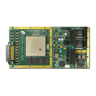
- Page 7 ADM-XRC-9R1B User Manual V1.1 - 14th October 2024 1 Introduction The ADM-XRC-9R1B is a high-performance 8 channel 6GSPS ADC and 8 channel 10GSPS DAC RF XMC for applications using Zynq Ultrascale+ RFSoC from Xilinx. Figure 1 : ADM-XRC-9R1-B Figure 2 : ADM-XRC-9R1-B...
- Page 8 ADM-XRC-9R1B User Manual V1.1 - 14th October 2024 1.1 Key Features Key Features • Single-width XMC, compliant to VITA Standard 42.0, 42.3 and 42.10d12 • Support for Zynq Ultrascale+ XCZU47DR/XCZU48DR/XQZU48DR RFSoC in FFVE1156 packages • Processing System (PS) Block consisting of: •...
- Page 9 Blank = Lead-free Lead /PB = Lead build Table 1 : Build Options Not all combinations are available. Please check with Alpha Data sales for details. 1.3 References & Specifications ANSI/VITA 42.0 XMC Standard, December 2008, VITA, ISBN 1-885731-49-3 ANSI/VITA 42.2 XMC Serial RapidIO Protocol Layer Standard, Feb 2006, VITA, ISBN 1-885731-41-8 ANSI/VITA 42.3...
- Page 10 ADM-XRC-9R1B User Manual V1.1 - 14th October 2024 2 RF Performance 2.1 Gen3 ADC Performance Measurement Conditions/Comments Value Unit Resolution Bits Sample Rate 1.0-5.0 GS/s Full Scale Input Voltage into RF connector (50R) @100MHz 1.20 Vpk-pk Full Scale Input Power into RF connector (50R) @100MHz...
- Page 11 ADM-XRC-9R1B User Manual V1.1 - 14th October 2024 Figure 3 : ADM-XRC-9R1B Gen3 RFSoC ADC Frequency Response Figure 4 : ADM-XRC-9R1B Gen3 RFSoC ADC Crosstalk RF Performance Page 5 ad-ug-1510_v1_1.pdf...
- Page 12 Table 4 : DAC Parameters [1]: Maximum sample rate depends on speed grade and SCD of RFSoC fitted. Figure 5 : ADM-XRC-9R1B Gen3 RFSoC DAC Frequency Response Figure 6 : ADM-XRC-9R1B Gen3 RFSoC DAC Crosstalk Page 6 RF Performance...
- Page 13 It can be used to program the RF clocks, drive signals from the DACs, receive data from the ADCs and control the RF converter settings using the Xilinx XRFDC API. Figure 7 : ADM-XRC-9R1B Vivado Example Design Example Design Page 7...
- Page 14 - Store in ESD safe bag. 4.1.2 Motherboard / Carrier Requirements The ADM-XRC-9R1B is a single width XMC.3 mezzanine with P6 and P4 connectors. The motherboard/ carrier must comply with the XMC.3 (VITA 42.3) specification for the Primary XMC connector, J5.
- Page 15 The power dissipation of the board is highly dependent on the Target FPGA application. A power estimator spreadsheet is available on request from Alpha Data. This should be used in conjunction with Xilinx power estimation tools to determine the exact current requirements for each power rail.
- Page 16 ADM-XRC-9R1B User Manual V1.1 - 14th October 2024 5 Functional Description 5.1 Overview Figure 8 : ADM-XRC-9R1B Block Diagram Page 10 Functional Description ad-ug-1510_v1_1.pdf...
- Page 17 ADM-XRC-9R1B User Manual V1.1 - 14th October 2024 5.1.1 Switch Definitions There is a set of eight DIP switches placed on the rear of the board. Their functions are described in Switch Definitions. Note: SW1-5 and SW1-8 are OFF by default. Factory Configuration switch must be in the OFF position for normal operation.
- Page 18 Pin low Table 6 : LED Definitions 5.1.2.1 User LEDs The user LEDs are attached to the CPLD and use an SPI interface to control them. The ADM-XRC-9R1B reference design provides VHDL code to control this interface. Page 12 Functional Description...
- Page 19 ADM-XRC-9R1B User Manual V1.1 - 14th October 2024 5.2 XMC Platform Interface 5.2.1 IPMI I2C A 2 Kbit I2C EEPROM (type M24C02) is connected to the XMC IPMI. This memory contains board information (type, voltage requirements etc.) as defined in the XMC based specification.
- Page 20 ADM-XRC-9R1B User Manual V1.1 - 14th October 2024 5.3 JTAG Interface 5.3.1 On-board Interface A JTAG boundary scan chain is connected to header U12. This allows the connection of the Xilinx JTAG cable for FPGA debug using the Xilinx ChipScope tools.
- Page 21 ADM-XRC-9R1B User Manual V1.1 - 14th October 2024 5.3.2 XMC Interface The JTAG interface on the XMC connector is normally unused and XMC_TDI connected directly to XMC_TDO. The interface can be connected to the on-board interface (through level-translators) by switching SW1-6 ON. See Switch Definitions 5.3.3 JTAG Voltages...
- Page 22 V1.1 - 14th October 2024 5.4 Clocks The ADM-XRC-9R1B provides a wide variety of clocking options. The board has a user-programmable clock generator. These clocks can be combined with the FPGA's internal PLLs to suit a wide variety of communication protocols.
- Page 23 ADM-XRC-9R1B User Manual V1.1 - 14th October 2024 Figure 13 : On-Board Digital System Clocks 5.4.1 300MHz Reference Clocks (REFCLK300M and FABRIC_CLK) The fixed 300MHz reference clocks REFCLK300M and FABRIC_CLK are differential LVDS signals. REFCLK300M is distributed through a fanout buffer, and is used as the input clock for both DDR4 SDRAM interfaces.
- Page 24 ADM-XRC-9R1B User Manual V1.1 - 14th October 2024 5.4.3 PN6 Reference Clock (PN6_PCIEREFCLK) The reference clock "PN6_PCIEREFCLK" is a differential clock provided by a carrier card through the Secondary XMC connector P6 at pins A19 and B19. This board connects this pair to an MGT clock input.
- Page 25 ADM-XRC-9R1B User Manual V1.1 - 14th October 2024 5.4.6 Digital System Oscillators There are four fixed oscillators on the board for the digital system. The USB and Ethernet reference clocks are used internally by the PHYs. Signal Frequency FPGA pin...
- Page 26 The RF reference clocks are generated with a dual-loop jitter cleaner PLL. The RF sampling clocks are provided by three LMX2594 RF clock synthesisers. Figure 15 : ADM-XRC-9R1B RF sampling clocks The external reference clock input amplitude to the LMK04208 is limited by slew rate as well as signal amplitude.
- Page 27 ADM-XRC-9R1B User Manual V1.1 - 14th October 2024 5.4.7.1 Sysref Clocks The sysref clocks provide the sysref functionality to synchronize the RF DACs and ADCs. They are provided by the RF clock generators. They are connected to the PL and the RF sampling block.
- Page 28 ADM-XRC-9R1B User Manual V1.1 - 14th October 2024 5.4.7.3 RF Clock Programming The RF reference clocks are programmed from the PL using SPI (LMX2594) or uWire (LMK04208). To minimise FPGA IO pin usage, a CPLD is used to multiplex a single 4-wire IO interface to the FPGA to each of the 4 devices.
- Page 29 5.5.4 PS DDR4 Memory The ADM-XRC-9R1B is fitted with one bank of PS DDR4 SDRAM. The bank is made up of a two 16-bit wide memory devices in parallel to provide a 32-bit datapath capable of running up to 1200MHz (DDR4-2400). 8Gbit devices (Micron MT40A512M16HA-083) are fitted as standard to provide 2GByte of memory.
- Page 30 Ports. The default speed of the COM ports is 115.2k. COM2 uses RS-232 by default but may be configured for RS-485 operation. Please contact Alpha Data for further details of the RS-485 mode. COM0 and COM2 are both connected to PS UART1, and are therefore mutually exclusive due to the PS only having two UART interfaces.
- Page 31 V1.1 - 14th October 2024 5.5.8 USB Interfaces The ADM-XRC-9R1B has two external USB interfaces connected to rear connector P4. The Zynq PS is configured as the USB host to the external interfaces. The on-board system monitor is accessible from the micro-USB connector...
- Page 32 The Target FPGA IO is arranged in banks, each with their own supply pins. The bank numbers, their voltage and function are shown in Target FPGA IO Banks. Full details of the IOSTANDARD required for each signal are given in the ADM-XRC-9R1B example design. IO Banks Voltage Purpose 3.3V...
- Page 33 V1.1 - 14th October 2024 5.6.3 Memory Interfaces The ADM-XRC-9R1B has two independent banks of DDR4 SDRAM. Each bank consists of one 8-bit wide memory device capable of running at up to 1200MHz (DDR-2400). 8Gbit devices (Micron MT40A1G8PM-083E) are fitted as standard.
- Page 34 ADM-XRC-9R1B User Manual V1.1 - 14th October 2024 5.7 RF Interfaces 5.7.1 Front-Panel I/O The front panel interface consists of a pair of 8-way high-speed locking connectors J3 and J4, and an IO mezzanine board with four SSMC connectors. These support 8 DAC signals, 8 ADC signals, two GPIO, an input RF reference clock, and an output RF reference clock.
- Page 35 ADM-XRC-9R1B User Manual V1.1 - 14th October 2024 Signal Impedance (Ohms) Pin number FPGA Pin ADC IO ERROR ADC0 J3-8 AK2/AK1 ADC1 J3-7 AH2/AH1 ADC2 J3-6 AF2/AF1 ADC3 J3-5 AD2/AD1 ADC4 J3-4 AB2/AB1 ADC5 J3-3 Y2/Y1 ADC6 J3-2 V2/V1 ADC7...
- Page 36 ADM-XRC-9R1B User Manual V1.1 - 14th October 2024 Figure 25 : RF Connector Pinout Page 30 Functional Description ad-ug-1510_v1_1.pdf...
- Page 37 Monitoring. 5.9 System Monitoring The ADM-XRC-9R1B has the ability to monitor temperature and voltage to maintain a check on the operation of the board. The monitoring is implemented using the Atmel AVR microcontroller. Control algorithms within the microcontroller automatically check line voltages and on board temperatures and shares the information with the PS.
- Page 38 ADM-XRC-9R1B User Manual V1.1 - 14th October 2024 5.9.1 Automatic Temperature Monitoring At power-up, the control logic sets the temperature limits and resets the LM87's over-temperature interrupt. The temperature limits are shown in Table Temperature Limits: FPGA Board Commercial 0 degC...
- Page 39 5.9.3 System Monitor Interfaces There are two ways to communicate with the System Monitor to retrieve board status information on the ADM-XRC-9R1B. One is through the Micro USB connector (shown in Interfaces), the other is using one of the PS UART interfaces (shown in Serial COM Ports).
- Page 40 ADM-XRC-9R1B User Manual V1.1 - 14th October 2024 Page Intentionally left blank Page 34 Functional Description ad-ug-1510_v1_1.pdf...
- Page 41 ROOT0_L Table 26 : Pn5 Interface *FPGA pins MRSTO_L and MBIST_L are disconnected by default (with MRSTO_L pulled high with a pull-up resistor). Please contact Alpha Data for further details if this is required. Rear Connector Pinouts Page 35 ad-ug-1510_v1_1.pdf...
- Page 42 ADM-XRC-9R1B User Manual V1.1 - 14th October 2024 Appendix A.2: Secondary XMC Connector, P6 PN6_TX_P0 PN6_TX_N0 P6_USB1_DP PN6_TX_P1 PN6_TX_N1 P6_COM1_RXD P6_USB1_DM P6_COM1_TXD PN6_TX_P2 PN6_TX_N2 P6_USB1_VBUS PN6_TX_P3 PN6_TX_N3 P6_COM2_TXP P6_USB2_DP P6_COM2_TXN PN6_TX_P4 PN6_TX_N4 P6_USB2_DM PN6_TX_P5 PN6_TX_N5 P6_COM2_RXP P6_USB2_VBUS P6_COM2_RXN PN6_TX_P6 PN6_TX_N6...
- Page 43 GP18 Table 28 : Pn6 GPIO Pin Map *FPGA pins K10 and K12 can optionally drive MRSTO# and MBIST# on the XMC P5 connector. Please contact Alpha Data for further details if this is required. Rear Connector Pinouts Page 37...
- Page 44 ADM-XRC-9R1B User Manual V1.1 - 14th October 2024 Appendix A.3: PMC Connector P4 Signal P4 Pin P4 Pin Signal P4_ETH0_MDI_0_P P4_ETH0_MDI_2_P P4_ETH0_MDI_0_N P4_ETH0_MDI_2_N P4_ETH0_MDI_1_P P4_ETH0_MDI_3_P P4_ETH0_MDI_1_N P4_ETH0_MDI_3_N P4_ETH1_MDI_0_P P4_ETH1_MDI_2_P P4_ETH1_MDI_0_N P4_ETH1_MDI_2_N P4_ETH1_MDI_1_P P4_ETH1_MDI_3_P P4_ETH1_MDI_1_N P4_ETH1_MDI_3_N P4_USB1_DM P4_USB2_DM P4_USB1_DP P4_USB2_DP P4_USB1_VBUS...
- Page 45 ADM-XRC-9R1B User Manual V1.1 - 14th October 2024 Revision History Date Revision Nature of Change Section(s) 27th September First Release. 2024 Section 5.6.4, 14th October Added info about GPIO pull-ups, added JTAG adapter picture Section 5.3 2024 Address: Suite L4A, 160 Dundee Street,...
Need help?
Do you have a question about the ADM-XRC-9R1B and is the answer not in the manual?
Questions and answers