Table of Contents
Advertisement
Quick Links
Advertisement
Table of Contents

Related Manuals for Alpha Data ADM-PCIE-7V3


Summary of Contents for Alpha Data ADM-PCIE-7V3
- Page 1 ADM-PCIE-7V3 Getting Started Guide Revision: V1.4 07/01/15...
- Page 2 ADM-PCIE-7V3 Getting Started Guide © 2014 Copyright Alpha Data Parallel Systems Ltd. All rights reserved. This publication is protected by Copyright Law, with all rights reserved. No part of this publication may be reproduced, in any shape or form, without prior written consent from Alpha Data Parallel Systems Ltd.
-
Page 3: Table Of Contents
OpenCL Reconfiguration ....................... 4 Partial Reconfiguration ........................4 Xilinx OpenCL ..........................5 Using the Alpha Data host API and Driver ..................6 Installing the driver ......................... 6 Building example host applications ....................7 Testing host examples with reference bitstreams ................7 FPGA Firmware Reference Designs ..................... -
Page 4: Introduction
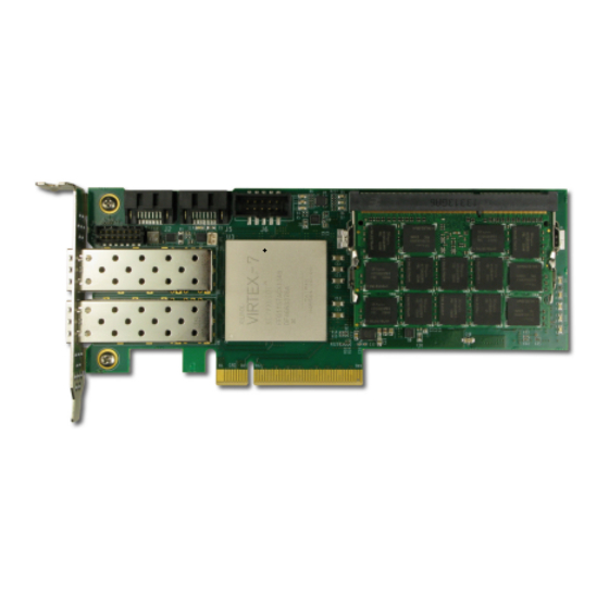
FPGA from flash and over JTAG, and accessing FPGA resources from host software. The ADM-PCIE-7V3 is designed to provide FPGA based accelerated computing to users in data centre and high performance computing applications. It has a high performance Gen3x8 PCIE interface for communication with the host. -
Page 5: Fpga Configuration Guide
This allows the user to select between bitstreams compatible with the Xilinx OpenCL API and the Alpha Data API, as well as allowing space for the user application bitstream and a failsafe bitstream (in case the user application bitstream has problems.) -
Page 6: Configuration Using Jtag
ADM-PCIE-7V3 Getting Started Guide Factory Switch Function OFF State ON State Default Failsafe/ SW1-3 Configure from failsafe region Configure from default region Default User SW1-4 Pin AB30 = '1' Pin AB30 = '0' Switch Table 1 : SW1 Switch Functions Power on configuration is the most reliable way to use the board, however it is also possible to reconfigure the board when powered on using a number of different methods. -
Page 7: Iprog Reconfiguration From Flash
ADM-PCIE-7V3 Getting Started Guide To configure the board using JTAG, first open Vivado 2014.3, and click on the "Open Hardware Manager" icon. Select "Open new hardware target" to run the Wizard and detect the Xilinx USB cable. If successful you... -
Page 8: Xilinx Opencl
ADM-PCIE-7V3 Getting Started Guide 3 Xilinx OpenCL This guide only covers a few basic points on the use of the board with Xilinx OpenCL. To use the board with Xilinx OpenCL, switch SW1-1 must be set to on to enable Xilinx mode. This will cause the board to boot up with the Xilinx OpenCL bitstream. -
Page 9: Using The Alpha Data Host Api And Driver
PCIe design, however this document assumes that the Alpha Data PCIe backend IP will be used. This core has the advantage that it includes extra board specific built in IP for communicating with the on-board flash, Product Data ROM and system monitoring chip, along with Direct Slave and Direct Master data transfer options. -
Page 10: Building Example Host Applications
All these applications except simple, will work with any bitstream built with the Alpha Data bridge IP. Other examples require the FPGA to be configured with a specific bitstream before running. - Page 11 0x00000000_00000000: 4321cbda ......!C.... [root@jura2 linux]# ./dump/dump wd 0 0 0x4 0x12345678 Window 0 offset 0x0 mapped @ 0x7ff89f56a000 0x0: 0x12345678 [root@jura2 linux]# ./dump/dump rd 0 0 0x4 Using the Alpha Data host API and Driver Page 8 ad-ug-0033_v1_4.pdf...
- Page 12 7. The monitor command can display real time voltage and temperature readings, however this functionality is not yet enabled with the current beta release of SDK 1.7.0 [root@jura2 linux]# ./monitor/monitor -? Usage: monitor [option ...] Option Type Default Meaning Using the Alpha Data host API and Driver Page 9 ad-ug-0033_v1_4.pdf...
- Page 13 [root@jura2 ~]# shutdown -r now ..[root@jura2 ~]# modprobe adb3 PciAddress64Bit=1 DmaMapLength=128 DmaMptlReadBurstLength=0x20 DmaMptlWriteBurstLength=0x20 [root@jura2 ~]# /opt/admxrcg3/admxrcg3sdk_apps-1.7.0b1/apps/linux/simpledma/simpledma Reading using DMA channel 0 at OCP address 0x0... Using the Alpha Data host API and Driver Page 10 ad-ug-0033_v1_4.pdf...
- Page 14 0x00000000_000000e0: 00000038 00000039 0000003a 0000003b 8...9...:...;... 0x00000000_000000f0: 0000003c 0000003d 0000003e 0000003f ..=..?... Measuring throughput... Throughput from host to FPGA is 3395.6 MiB/s Throughput from FPGA to host is 5204.4 MiB/s PASSED Using the Alpha Data host API and Driver Page 11 ad-ug-0033_v1_4.pdf...
-
Page 15: Fpga Firmware Reference Designs
ADM-PCIE-7V3 Getting Started Guide 5 FPGA Firmware Reference Designs 5.1 A Tutorial on building Xilinx IP In this section the customisation of standard Xilinx IP for use with the board is demonstarted 5.1.1 Building MIG (Memory Interface Generator) Open Vivado and Select "create new project"... - Page 16 ADM-PCIE-7V3 Getting Started Guide On the first option page, select Create Design, and change the number of Controllers to 2. On the controller options pages, Select 1500ps for the Clock Period. This will configure the controller to run the external memory at 1333MHz. For the memory type, select SODIMMs, and select the MT18KSF1G72HZ-1G6 part.
- Page 17 ADM-PCIE-7V3 Getting Started Guide On the memory options page set the input clock period to 2500ps (400MHz) and change RTT to RZQ/6 Leave FPGA options unchanged In Pin/Bank Selection Mode, select Fixed Pin Out FPGA Firmware Reference Designs Page 14...
- Page 18 Select Next, Accept the terms and conditions until finally you are given the option to generate the core. The ADM-PCIE-7V3 requires a couple of extra signals to drive out logic 1 on 2 pins to turn on the power supplied for the DRAM interfaces.
- Page 19 ADM-PCIE-7V3 Getting Started Guide set_property PACKAGE_PIN AA24 [get_ports dram_0_on] set_property IOSTANDARD LVCMOS18 [get_ports dram_0_on] set_property PACKAGE_PIN AB25 [get_ports dram_1_on] set_property IOSTANDARD LVCMOS18 [get_ports dram_1_on] FPGA Firmware Reference Designs Page 16 ad-ug-0033_v1_4.pdf...
-
Page 20: Axi-4 Reference Designs Demonstrating Pcie And Memory
5.2.1 Basic AXI-4 PCIE Reference Design A basic PCIe reference design is provided showing how to connect up the Alpha Data PCIe core to other AXI-4 modules in the system. The AXI-4 profile provided by the core is fixed to being 256 data bits wide, 39 address bits, running at 250MHz. - Page 21 ADM-PCIE-7V3 Getting Started Guide simple design demonstrates how both Direct Slave (register accesses) and DMA (high performance data transfers) can access modules in an AXI-4 system. The AXI-4 system has been built using IP Integrator, with the block diagram editor handling the complexities of AXI-4 bus connection.
-
Page 22: Axi-4 Reference Design With Memory Interfaces
ADM-PCIE-7V3 Getting Started Guide 0x00007faf_0xab50e0b0: 00000000 00000000 00000000 00000000 ....0x00007faf_0xab50e0c0: 00000000 00000000 00000000 00000000 ....0x00007faf_0xab50e0d0: 00000000 00000000 00000000 00000000 ....0x00007faf_0xab50e0e0: 00000000 00000000 00000000 00000000 ....0x00007faf_0xab50e0f0: 00000000 00000000 00000000 00000000 ....dmadump can also be used to test out the memory accessing it via the DMA engine. -
Page 23: Figure 4 Top Level Architecture Of Sodimm Reference Design
ADM-PCIE-7V3 Getting Started Guide LEDS AXI4 To AXI4 To BRAM0 BRAM BRAM BRAM SODIMM AXI4 Crossbar SODIMM Controller Controller AXI4 To BRAM1 BRAM AXI4 Lite Crossbar AXI4 To AXI4 Crossbar Lite DMA(x1) AXI-4 AD AXI-4 PCIe Lite Gen3 Core PCIe Gen3x8... -
Page 24: Table 2 Memory Map Ds_Axi (39 Address Bits = 512G)
ADM-PCIE-7V3 Getting Started Guide AXI4 Block Interface Offset Address Range High Address BRAM1 S_AXI 0x0000000000 0x0000001FFF mig_7series_0 S0_AXI_CTRL 0x0000100000 0x00001FFFFF mig_7series_0 S1_AXI_CTRL 0x0000200000 0x00002FFFFF mig_7series_0 S0_AXI 0x1200000000 0x13FFFFFFFF mig_7series_0 S1_AXI 0x1400000000 0x15FFFFFFFF BRAM0 S_AXI 0x1000000000 0x100000FFFF Table 2 : Memory Map DS_AXI (39 address bits = 512G) - Page 25 ADM-PCIE-7V3 Getting Started Guide 0x00007feb_0x12262010: deaddead deaddead deaddead deaddead ....0x00007feb_0x12262020: deaddead deaddead deaddead deaddead ....0x00007feb_0x12262030: deaddead deaddead deaddead deaddead ....The Direct Slave window in the hosts memory map is limited to 4MB, so the upper addresses are not directly available.
- Page 26 ADM-PCIE-7V3 Getting Started Guide applications. To access the other SDRAM area, the start address needs to be set to 0x1200000000 or 0x1400000000. After accessing the higher addresses, the page register can be cleared to allow access to the BRAM again.
- Page 27 ADM-PCIE-7V3 Getting Started Guide 0x00000002_000000E0: 00000000 00000000 00000000 00000000 ....0x00000002_000000F0: FFFFFFFF FFFFFFFF FFFFFFFF FFFFFFFF ....simpledma can again be used to measure the DMA performance from the BRAM or a SODIMM [root@jura2 simpledma]# ./simpledma -n 0 Reading using DMA channel 0 at OCP address 0x0...
-
Page 28: Sdk Fpga Designs
ADM-PCIE-7V3 Getting Started Guide 5.3 SDK FPGA Designs The reference bitstreams included in the SDK 1.7.0 are based upon designs used in previous Alpha-Data cards. The HDL modules in these are connected together using a protocol profile conforming to the OCP standard. -
Page 29: Troubleshooting Guide
In this case it is also worth checking with lspci which should produce the following expected output. [root@jura2 ~]# lspci -vvv -d 4144:adb3 01:00.0 Bridge: Alpha Data Device adb3 (rev 01) Subsystem: Alpha Data Device 0706 Control: I/O- Mem- BusMaster- SpecCycle- MemWINV- VGASnoop- ParErr- Stepping- SERR- FastB2B- DisINTx- Status: Cap+ 66MHz- UDF- FastB2B- ParErr- DEVSEL=fast >TAbort- <TAbort- <... -
Page 30: Figure 5 Leds
ADM-PCIE-7V3 Getting Started Guide Capabilities: [100 v2] Advanced Error Reporting UESta: DLP- SDES- TLP- FCP- CmpltTO- CmpltAbrt- UnxCmplt- RxOF- MalfTLP- ECRC- UnsupReq- ACSViol- UEMsk: DLP- SDES- TLP- FCP- CmpltTO- CmpltAbrt- UnxCmplt- RxOF- MalfTLP- ECRC- UnsupReq- ACSViol- UESvrt: DLP+ SDES+ TLP- FCP+ CmpltTO- CmpltAbrt- UnxCmplt- RxOF+... -
Page 31: Access Denied
ADM-PCIE-7V3 Getting Started Guide 6.2 Access Denied Another common error code that may occur is access denied *** Failed to open card with index 0: ADMXRC3_ACCESS_DENIED This is the result of a non-root user trying to run a program containing an API function that requires root (Administrator) privileges. - Page 32 ADM-PCIE-7V3 Getting Started Guide Revision History Date Revision Nature of Change 26/05/14 21/08/14 20/10/14 updated to use IPI PCIe cores 13/11/14 added links to release SDK 1.7.0 07/01/15 modified designs to support 2014.4 Address: 4 West Silvermills Lane, Address: 3507 Ringsby Court Suite 105,...
Need help?
Do you have a question about the ADM-PCIE-7V3 and is the answer not in the manual?
Questions and answers