Table of Contents
Advertisement
Quick Links
Advertisement
Table of Contents

Related Manuals for Alpha Data ADM-PA101


Summary of Contents for Alpha Data ADM-PA101
- Page 1 ADM-PA101 User Manual Document Revision: 1.2 December 13th 2021...
- Page 2 ADM-PA101 User Manual © 2021 Copyright Alpha Data Parallel Systems Ltd. All rights reserved. This publication is protected by Copyright Law, with all rights reserved. No part of this publication may be reproduced, in any shape or form, without prior written consent from Alpha Data Parallel Systems Ltd.
-
Page 3: Table Of Contents
ADM-PA101 User Manual Table Of Contents Introduction ............................1 Key Features ..........................1 Order Code ............................ 2 Board Information ..........................3 Physical Specifications ........................3 Chassis Requirements ........................4 2.2.1 PCI Express ..........................4 2.2.2 Mechanical Requirements ......................4 2.2.3 Power Requirements ......................... - Page 4 Table 10 MIO Map ............................25 Table 11 Complete Pinout Table ........................28 List of Figures Figure 1 ADM-PA101 Product Photo ....................... 1 Figure 2 Thermal Performance ........................5 Figure 3 ADM-PA101 Block Diagram ....................... 6 Figure 4 Switches ............................7 Figure 5 Front Panel LEDs ..........................
-
Page 5: Introduction
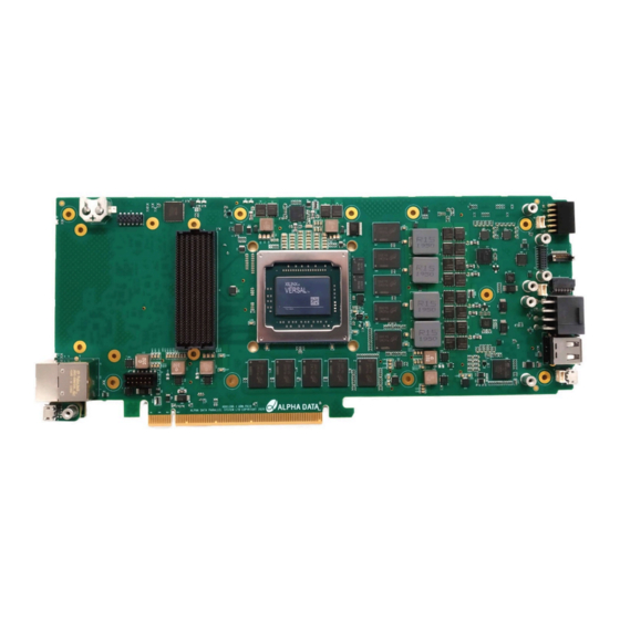
ADM-PA101 User Manual 1 Introduction The ADM-PA101 is a high-performance reconfigurable computing card featuring the latest Xilinx Adaptive Compute Acceleration Platform (ACAP) platform known as Versal. The PCIe form factor is ideal for Data Center applications and general evaluation and deployment of this new architecture. The card features a full FMC+ interface, two banks of 72-bit DDR4-SDRAM, front panel Ethernet, PMOD, USB, and Samtec FireFly. -
Page 6: Order Code
ADM-PA101 User Manual 1.2 Order Code See the PA101 datasheet for complete ordering options. Page 2 Introduction ad-ug-1430_v1_2.pdf... -
Page 7: Board Information
ADM-PA101 User Manual 2 Board Information 2.1 Physical Specifications The ADM-PA101 complies with PCI Express CEM revision 4.0. Description Measure Total Dy 126.3 mm PCB Dy 111.15 mm Total Dx 267.2 mm PCB Dx 254 mm Total Dz 19.6 mm... -
Page 8: Chassis Requirements
2.2.3 Power Requirements The ADM-PA101 draws power from the PCIe Edge and the 8-pin ATX power connector. The ADM-PA101 does not use or require the 3.3V power from the PCIe Edge (though it does use 3.3V AUX). To operate with PCIe edge only, ensure SW1-8 is OFF (see Switches). -
Page 9: Thermal Performance
The ADM-PA101 comes with a heat sink to avoid thermal overstress of ACAP, since it is typically the hottest point on the card. The ACAP die temperature must remain under 100 degrees Celsius. To estimate the ACAP die temperature: first take your total board power (see next paragraph), then multiply by Theta JA from the graph below, and add the resulting temperature to your system internal ambient temperature. -
Page 10: Functional Description
3 Functional Description 3.1 Overview The ADM-PA101 is a high-performance reconfigurable computing card featuring the latest Xilinx Adaptive Compute Acceleration Platform (ACAP) platform with the Versal XCVC1902, a full FMC+ interface, PCIe Gen3x16 or 2xGen4x8 interface, two banks of DDR4-3200 each 72 bits wide (for 64 bits with 8 bits ECC), GEM0 Ethernet, QSPI, uSD, USB, UART, a Digilent PMOD site, one Samtec FireFly site capable of 28G/channel in either optical or copper cabling, and a robust system monitor. -
Page 11: Switches
ADM-PA101 User Manual 3.1.1 Switches The ADM-PA101 has two octal DIP switch SW1 and SW2, located on the rear side of the board. The function of each switch is detailed below: Figure 4 : Switches Factory Switch Function OFF State... -
Page 12: Leds
ADM-PA101 User Manual 3.1.2 LEDs There are 6 LEDs on the ADM-PA101, 2 of which are general purpose and whose meaning can be defined by the user. The other 4 have fixed functions described below: User LEDs Status LEDs DONE_L STAT_1... -
Page 13: Clocking
ADM-PA101 User Manual 3.2 Clocking The ADM-PA101 provides flexible reference clock solutions for the many multi-gigabit transceiver quads, DDR4 banks, and PL fabric. Any programmable clock, from the Si5338 Clock Synthesizer, is reconfigurable from the front panel Micro USB Interface by using Alpha Data’s avr2util utility. -
Page 14: Si5328
ADM-PA101 User Manual 3.2.1 Si5328 If jitter attenuation is required please see the reference documentation for the Si5328. www.silabs.com/Support%20Documents/TechnicalDocs/Si5328.pdf There are two input clock options. Si5328 pin CLKIN1 (board net name SI5328_REFCLK_IN_P/N) of the Si5328 is connected to an MGT clock output for the most direct clock recovery architecture. Si5328 pin CLKIN2 (board net name MGT_PROGCLK_6_P/N) of the Si5328 is connected to a programable clock from the onboard clock synthesizer. -
Page 15: Fmc Clocks
ADM-PA101 User Manual quad. This programable clock has a default 156.25MHz reference clock. This clock frequency can be changed to any arbitrary clock frequency up to 350MHz by re-programing the Si5338 reprogrammable clock oscillator. See details on avr2util in the section: Micro USB Interface. -
Page 16: Pci Express
ADM-PA101 User Manual 3.3 PCI Express The ADM-PA100 is capable of PCIe Gen 1/2/3 with 1/4/8/16 lanes and Gen 4 with 1/4/8 lanes. The ACAP drives these lanes directly using the Integrated PCI Express block from Xilinx. Negotiation of PCIe link speed and number of lanes is generally automatic and does not require user intervention. -
Page 17: Fmc+ Interface
Note: The ADM-PA101 supports only 1.5V and lower VADJ Voltages. The ADM-PA101 provides additional keep out space in the FMC area to enable oversized FMC cards. This is ideal for pluggable optical modules like QSFP-DD. See Alpha Data FMC-PLUS-QSFP-DD for one example. -
Page 18: Fmc+ Groups
ADM-PA101 User Manual The FMC+ Connector has GPIO connections arranged as follows: ACAP Group Name Function Bank LA(12:2) 11 diff. Pairs / 22 single-ended LA_0 LA_CC (1:0) 2x Regional Clocks / GPIO pairs / 4 single-ended LA(33:19) 15 diff. Pairs / 30 single-ended... -
Page 19: Firefly
ADM-PA101 User Manual 3.6 FireFly There is one FireFly site available on the circuit board. The site is capable of hosting either active optical or passive copper FireFly connectors. The communication interface can run at up to 28Gbps per channel in either cable type. -
Page 20: System Monitor
ADM-PA101 User Manual 3.7 System Monitor The ADM-PA101 has the ability to monitor select temperatures, voltages, and currents in order to provide an indication of board health. The monitoring is implemented using an AVR microcontroller. This information can be read out via USB using the avr2util utility. Alternatively, the sensor information can be read directly by the ACAP or via PCIe if RD-PA101 is purchased (reference design package). -
Page 21: System Monitor Status Leds
ADM-PA101 User Manual 3.7.1 System Monitor Status LEDs LEDs D14 (Red) and D15 (Green) indicate the card health status. LEDs Status Green Running and no alarms Green + Red Standby (Powered off) Flashing Green + Flashing Red Attention - critical alarm active... -
Page 22: Micro Usb Interface
The ADM-PA101 utilizes the Digilent USB-JTAG converter which is supported by the Xilinx software tool suite. Simply connect a micro-USB AB type cable between the ADM-PA101 USB port and a host computer with Vivado installed. Vivado Hardware Manager will automatically recognize the ACAP and allow you to configure the ACAP and the SPI configuration Flash memory. -
Page 23: Configuration
SPI device (2x Micron part number MT25QU01GCBB8E12). The ADM-PA101 is shipped with a simple PCIe endpoint bitstream which should be visible to the operating system (using Windows Device Manager or “lspci” in Linux) in order to provide confidence that the card is working correctly when installed in a system. -
Page 24: Building And Programming Usd Configuration Images
Figure 11 : uSD Location The ADM-PA101 is shipped with a simple PCIe endpoint bitstream which should be visible to the operating system (using Windows Device Manager or “lspci” in Linux) in order to provide confidence that the card is working correctly when installed in a system. -
Page 25: Table 9 Boot Mode Selection
ADM-PA101 User Manual MODE3 MODE2 MODE1 MODE0 Boot Mode (SW1-4) (SW1-3) (SW1-2) (SW1-1) JTAG Quad SPI (24 bit addressing) Quad SPI (32 bit addressing) SD Flash - SD 3.0 Table 9 : Boot Mode Selection Note: all other possible switch settings are reserved / invalid. -
Page 26: Ulpi Usb Interface
USB cable. This UART interface will appear in the host system as soon as the USB cable is installed, even before the ADM-PA101 is powered up. This interface is suitable to capture power-on messages from the processor. -
Page 27: Gem0
WP, SDA, and SCL signals all have external pull-up resistors on the card. 3.14 PMOD The ADM-PA101 includes a twelve-pin right angle connector PMOD host interface at the rear edge of the card with a full 0.9" clearance. This interface is connected to the PL of the ACAP. - Page 28 ADM-PA101 User Manual Page Intentionally left blank Page 24 Functional Description ad-ug-1430_v1_2.pdf...
-
Page 29: Appendix A Mio Map
ADM-PA101 User Manual Appendix A: MIO Map Pin Number Pin Name Signal Name Comment PMC_MIO0_500 QSPI0_CLK Dual-Parallel Quad SPI PMC_MIO1_500 QSPI0_IO[1] Dual-Parallel Quad SPI PMC_MIO2_500 QSPI0_IO[2] Dual-Parallel Quad SPI PMC_MIO3_500 QSPI0_IO[3] Dual-Parallel Quad SPI PMC_MIO4_500 QSPI0_IO[0] Dual-Parallel Quad SPI PMC_MIO5_500... - Page 30 ADM-PA101 User Manual Pin Number Pin Name Signal Name Comment PMC_MIO34_501 SD1_SEL SD1_3.0 PMC_MIO35_501 SD1_DIR_CMD SD1_3.0 PMC_MIO36_501 SD1_ DIR0 SD1_3.0 PMC_MIO37_501 GEM0_RST_L GEM0 Ethernet PMC_MIO38_501 PCIE_PERST_B PCIE PMC_MIO39_501 ERROR PMC_MIO40_501 ERROR PMC_MIO41_501 ERROR PMC_MIO42_501 UART0_RXD Not availabe until full power...
-
Page 31: Table 10 Mio Map
ADM-PA101 User Manual Pin Number Pin Name Signal Name Comment LPD_MIO18_502 GPIO GPIO J4 at rear LPD_MIO19_502 GPIO GPIO J4 at rear LPD_MIO20_502 GPIO GPIO J4 at rear LPD_MIO21_502 GPIO GPIO J4 at rear LPD_MIO22_502 GPIO GPIO J4 at rear... -
Page 32: Appendix B Complete Pinout Table
ADM-PA101 User Manual Appendix B: Complete Pinout Table Signal Name Pin Name IO Voltage Number AVR_B2U IO_L1P_406 AVR_MON_CLK IO_L2P_406 AVR_U2B IO_L1N_406 BB24 CLK0_M2C_PIN_N IO_L24N_GC_XCC_N8P1_M2P49_706 BA24 CLK0_M2C_PIN_P IO_L24P_GC_XCC_N8P0_M2P48_706 BA12 CLK1_M2C_PIN_N IO_L24N_GC_XCC_N8P1_M2P157_708 AY13 CLK1_M2C_PIN_P IO_L24P_GC_XCC_N8P0_M2P156_708 BD22 CLK2_BIDIR_PIN_N IO_L9N_GC_XCC_N3P1_M2P19_706 BC23 CLK2_BIDIR_PIN_P IO_L9P_GC_XCC_N3P0_M2P18_706 AW23... -
Page 33: Table
ADM-PA101 User Manual Signal Name Pin Name IO Voltage Number AF41 DDR4_0_CLK_C IO_L15N_XCC_N5P1_M0P31_700 AG41 DDR4_0_CLK_T IO_L15P_XCC_N5P0_M0P30_700 AH40 DDR4_0_CS_N IO_L14P_N4P4_M0P28_700 AN42 DDR4_0_DEBUG IO_L26P_N8P4_M0P106_701 AP40 DDR4_0_DM0 IO_L18P_XCC_N6P0_M0P90_701 AK40 DDR4_0_DM1 IO_L12P_GC_XCC_N4P0_M0P78_701 AF47 DDR4_0_DM2 IO_L0P_XCC_N0P0_M0P0_700 AH43 DDR4_0_DM3 IO_L6P_GC_XCC_N2P0_M0P12_700 AN46 DDR4_0_DM4 IO_L0P_XCC_N0P0_M0P54_701 AT47 DDR4_0_DM5 IO_L9P_GC_XCC_N3P0_M0P72_701... -
Page 34: Table
ADM-PA101 User Manual Signal Name Pin Name IO Voltage Number AD44 DDR4_0_DQ29 IO_L7P_N2P2_M0P14_700 AP39 DDR4_0_DQ3 IO_L23P_N7P4_M0P100_701 AJ45 DDR4_0_DQ30 IO_L8N_N2P5_M0P17_700 AE44 DDR4_0_DQ31 IO_L7N_N2P3_M0P15_700 AL44 DDR4_0_DQ32 IO_L4N_N1P3_M0P63_701 AM46 DDR4_0_DQ33 IO_L5P_N1P4_M0P64_701 AM45 DDR4_0_DQ34 IO_L2N_N0P5_M0P59_701 AL46 DDR4_0_DQ35 IO_L1P_N0P2_M0P56_701 AL43 DDR4_0_DQ36 IO_L4P_N1P2_M0P62_701 AL47 DDR4_0_DQ37 IO_L1N_N0P3_M0P57_701... - Page 35 ADM-PA101 User Manual Signal Name Pin Name IO Voltage Number BE45 DDR4_0_DQ60 IO_L10N_N3P3_M0P129_702 AV45 DDR4_0_DQ61 IO_L7N_N2P3_M0P123_702 BC45 DDR4_0_DQ62 IO_L8P_N2P4_M0P124_702 AW45 DDR4_0_DQ63 IO_L11N_N3P5_M0P131_702 BD42 DDR4_0_DQ64 IO_L16P_N5P2_M0P140_702 AW42 DDR4_0_DQ65 IO_L17P_N5P4_M0P142_702 BC43 DDR4_0_DQ66 IO_L14N_N4P5_M0P137_702 AW43 DDR4_0_DQ67 IO_L17N_N5P5_M0P143_702 BE42 DDR4_0_DQ68 IO_L16N_N5P3_M0P141_702 AV43 DDR4_0_DQ69 IO_L13N_N4P3_M0P135_702...
- Page 36 ADM-PA101 User Manual Signal Name Pin Name IO Voltage Number AD37 DDR4_0_RAS_N IO_L19N_N6P3_M0P39_700 AK42 DDR4_0_RESET_N IO_L25P_N8P2_M0P104_701 BE27 DDR4_1_A0 IO_L3P_XCC_N1P0_M1P114_705 BC26 DDR4_1_A1 IO_L8N_N2P5_M1P125_705 BG28 DDR4_1_A10 IO_L0N_XCC_N0P1_M1P109_705 AV29 DDR4_1_A11 IO_L25P_N8P2_M1P158_705 AP27 DDR4_1_A12 IO_L21N_XCC_N7P1_M1P151_705 AY27 DDR4_1_A13 IO_L24N_GC_XCC_N8P1_M1P157_705 BB28 DDR4_1_A14 IO_L7N_N2P3_M1P123_705 BD29 DDR4_1_A15 IO_L11N_N3P5_M1P131_705...
- Page 37 ADM-PA101 User Manual Signal Name Pin Name IO Voltage Number AW36 DDR4_1_DM7 IO_L15P_XCC_N5P0_M1P30_703 AT38 DDR4_1_DM8 IO_L18P_XCC_N6P0_M1P36_703 AT29 DDR4_1_DQ0 IO_L13P_N4P2_M1P134_705 AU25 DDR4_1_DQ1 IO_L16P_N5P2_M1P140_705 AP25 DDR4_1_DQ10 IO_L22N_N7P3_M1P153_705 AM27 DDR4_1_DQ11 IO_L23P_N7P4_M1P154_705 AM26 DDR4_1_DQ12 IO_L20P_N6P4_M1P148_705 AM29 DDR4_1_DQ13 IO_L19P_N6P2_M1P146_705 AN25 DDR4_1_DQ14 IO_L22P_N7P2_M1P152_705 AN28 DDR4_1_DQ15 IO_L23N_N7P5_M1P155_705...
- Page 38 ADM-PA101 User Manual Signal Name Pin Name IO Voltage Number BB31 DDR4_1_DQ39 IO_L7P_N2P2_M1P68_704 AR29 DDR4_1_DQ4 IO_L17P_N5P4_M1P142_705 BC33 DDR4_1_DQ40 IO_L4N_N1P3_M1P63_704 BE35 DDR4_1_DQ41 IO_L1P_N0P2_M1P56_704 BD34 DDR4_1_DQ42 IO_L2N_N0P5_M1P59_704 BF34 DDR4_1_DQ43 IO_L1N_N0P3_M1P57_704 BB34 DDR4_1_DQ44 IO_L4P_N1P2_M1P62_704 BG35 DDR4_1_DQ45 IO_L5P_N1P4_M1P64_704 BD35 DDR4_1_DQ46 IO_L2P_N0P4_M1P58_704 BG34 DDR4_1_DQ47 IO_L5N_N1P5_M1P65_704...
- Page 39 ADM-PA101 User Manual Signal Name Pin Name IO Voltage Number AT35 DDR4_1_DQ70 IO_L20N_N6P5_M1P41_703 AP38 DDR4_1_DQ71 IO_L23P_N7P4_M1P46_703 AN26 DDR4_1_DQ8 IO_L20N_N6P5_M1P149_705 AN29 DDR4_1_DQ9 IO_L19N_N6P3_M1P147_705 AV27 DDR4_1_DQS0_C IO_L12N_GC_XCC_N4P1_M1P133_705 AU28 DDR4_1_DQS0_T IO_L12P_GC_XCC_N4P0_M1P132_705 AR27 DDR4_1_DQS1_C IO_L18N_XCC_N6P1_M1P145_705 AP28 DDR4_1_DQS1_T IO_L18P_XCC_N6P0_M1P144_705 AT32 DDR4_1_DQS2_C IO_L15N_XCC_N5P1_M1P85_704 AU32 DDR4_1_DQS2_T IO_L15P_XCC_N5P0_M1P84_704...
- Page 40 ADM-PA101 User Manual Signal Name Pin Name IO Voltage Number DP10_C2M_P GTY_TXP2_202 DP10_M2C_N GTY_RXN2_202 DP10_M2C_P GTY_RXP2_202 DP11_C2M_N GTY_TXN3_202 DP11_C2M_P GTY_TXP3_202 DP11_M2C_N GTY_RXN3_202 DP11_M2C_P GTY_RXP3_202 DP12_C2M_N GTY_TXN0_203 DP12_C2M_P GTY_TXP0_203 DP12_M2C_N GTY_RXN0_203 DP12_M2C_P GTY_RXP0_203 DP13_C2M_N GTY_TXN1_203 DP13_C2M_P GTY_TXP1_203 DP13_M2C_N GTY_RXN1_203 DP13_M2C_P GTY_RXP1_203...
- Page 41 ADM-PA101 User Manual Signal Name Pin Name IO Voltage Number DP19_C2M_N GTY_TXN3_204 DP19_C2M_P GTY_TXP3_204 DP19_M2C_N GTY_RXN3_204 DP19_M2C_P GTY_RXP3_204 DP2_C2M_N GTY_TXN2_200 DP2_C2M_P GTY_TXP2_200 DP2_M2C_N GTY_RXN2_200 DP2_M2C_P GTY_RXP2_200 DP20_C2M_N GTY_TXN0_205 DP20_C2M_P GTY_TXP0_205 DP20_M2C_N GTY_RXN0_205 DP20_M2C_P GTY_RXP0_205 DP21_C2M_N GTY_TXN1_205 DP21_C2M_P GTY_TXP1_205 DP21_M2C_N GTY_RXN1_205...
- Page 42 ADM-PA101 User Manual Signal Name Pin Name IO Voltage Number DP5_M2C_P GTY_RXP1_201 DP6_C2M_N GTY_TXN2_201 DP6_C2M_P GTY_TXP2_201 DP6_M2C_N GTY_RXN2_201 DP6_M2C_P GTY_RXP2_201 DP7_C2M_N GTY_TXN3_201 DP7_C2M_P GTY_TXP3_201 DP7_M2C_N GTY_RXN3_201 DP7_M2C_P GTY_RXP3_201 DP8_C2M_N GTY_TXN0_202 DP8_C2M_P GTY_TXP0_202 DP8_M2C_N GTY_RXN0_202 DP8_M2C_P GTY_RXP0_202 DP9_C2M_N GTY_TXN1_202 DP9_C2M_P GTY_TXP1_202...
- Page 43 ADM-PA101 User Manual Signal Name Pin Name IO Voltage Number FIREFLY_SCL IO_L8N_406 FIREFLY_SDA IO_L8P_406 FIREFLY_TX0_N GTY_TXN0_206 FIREFLY_TX0_P GTY_TXP0_206 FIREFLY_TX1_N GTY_TXN1_206 FIREFLY_TX1_P GTY_TXP1_206 FIREFLY_TX2_N GTY_TXN2_206 FIREFLY_TX2_P GTY_TXP2_206 FIREFLY_TX3_N GTY_TXN3_206 FIREFLY_TX3_P GTY_TXP3_206 FPGA_SYSMON_I2C_SCL PMC_MIO44_501 FPGA_SYSMON_I2C_SDA PMC_MIO45_501 GBTCLK2_PIN_N GTY_REFCLKN1_202 MGT REFCLK GBTCLK2_PIN_P GTY_REFCLKP1_202...
- Page 44 ADM-PA101 User Manual Signal Name Pin Name IO Voltage Number BD13 HA01_CC_N IO_L9N_GC_XCC_N3P1_M2P127_708 FMC_VADJ BC13 HA01_CC_P IO_L9P_GC_XCC_N3P0_M2P126_708 FMC_VADJ AU15 HA02_N IO_L13N_N4P3_M2P135_708 FMC_VADJ AT14 HA02_P IO_L13P_N4P2_M2P134_708 FMC_VADJ AN13 HA03_N IO_L21N_XCC_N7P1_M2P151_708 FMC_VADJ AP12 HA03_P IO_L21P_XCC_N7P0_M2P150_708 FMC_VADJ AT11 HA04_N IO_L22N_N7P3_M2P153_708 FMC_VADJ AR11 HA04_P...
- Page 45 ADM-PA101 User Manual Signal Name Pin Name IO Voltage Number BB15 HA18_P IO_L7P_N2P2_M2P122_708 FMC_VADJ BD14 HA19_N IO_L11N_N3P5_M2P131_708 FMC_VADJ BD15 HA19_P IO_L11P_N3P4_M2P130_708 FMC_VADJ BG11 HA20_N IO_L4N_N1P3_M2P117_708 FMC_VADJ BF11 HA20_P IO_L4P_N1P2_M2P116_708 FMC_VADJ BF13 HA21_N IO_L3N_XCC_N1P1_M2P115_708 FMC_VADJ BE12 HA21_P IO_L3P_XCC_N1P0_M2P114_708 FMC_VADJ BG13 HA22_N...
- Page 46 ADM-PA101 User Manual Signal Name Pin Name IO Voltage Number HB12_N IO_L16N_N5P3_M3P33_709 FMC_VADJ HB12_P IO_L16P_N5P2_M3P32_709 FMC_VADJ HB13_N IO_L20N_N6P5_M3P41_709 FMC_VADJ BC10 HB13_P IO_L20P_N6P4_M3P40_709 FMC_VADJ HB14_N IO_L7N_N2P3_M3P15_709 FMC_VADJ HB14_P IO_L7P_N2P2_M3P14_709 FMC_VADJ HB15_N IO_L1N_N0P3_M3P3_709 FMC_VADJ HB15_P IO_L1P_N0P2_M3P2_709 FMC_VADJ HB16_N IO_L15N_XCC_N5P1_M3P31_709 FMC_VADJ HB16_P IO_L15P_XCC_N5P0_M3P30_709...
- Page 47 ADM-PA101 User Manual Signal Name Pin Name IO Voltage Number AV19 LA07_P IO_L26P_N8P4_M2P106_707 FMC_VADJ AU16 LA08_N IO_L22N_N7P3_M2P99_707 FMC_VADJ AT17 LA08_P IO_L22P_N7P2_M2P98_707 FMC_VADJ AN17 LA09_N IO_L19N_N6P3_M2P93_707 FMC_VADJ AM18 LA09_P IO_L19P_N6P2_M2P92_707 FMC_VADJ AR17 LA10_N IO_L18N_XCC_N6P1_M2P91_707 FMC_VADJ AT16 LA10_P IO_L18P_XCC_N6P0_M2P90_707 FMC_VADJ AP16 LA11_N...
- Page 48 ADM-PA101 User Manual Signal Name Pin Name IO Voltage Number BE20 LA25_N IO_L4N_N1P3_M2P9_706 FMC_VADJ BE21 LA25_P IO_L4P_N1P2_M2P8_706 FMC_VADJ BF17 LA26_N IO_L8N_N2P5_M2P71_707 FMC_VADJ BE16 LA26_P IO_L8P_N2P4_M2P70_707 FMC_VADJ BE24 LA27_N IO_L7N_N2P3_M2P15_706 FMC_VADJ BE25 LA27_P IO_L7P_N2P2_M2P14_706 FMC_VADJ BF22 LA28_N IO_L3N_XCC_N1P1_M2P7_706 FMC_VADJ BG21 LA28_P...
- Page 49 ADM-PA101 User Manual Signal Name Pin Name IO Voltage Number AY31 MEM_CLK_1_PIN_P IO_L24P_GC_XCC_N8P0_M1P102_704 AF10 MGT_PROGCLK_0_PIN_N GTY_REFCLKN0_200 MGT REFCLK AF11 MGT_PROGCLK_0_PIN_P GTY_REFCLKP0_200 MGT REFCLK AB10 MGT_PROGCLK_1_PIN_N GTY_REFCLKN0_201 MGT REFCLK AB11 MGT_PROGCLK_1_PIN_P GTY_REFCLKP0_201 MGT REFCLK MGT_PROGCLK_2_PIN_N GTY_REFCLKN0_202 MGT REFCLK MGT_PROGCLK_2_PIN_P GTY_REFCLKP0_202 MGT REFCLK...
- Page 50 ADM-PA101 User Manual Signal Name Pin Name IO Voltage Number AA44 PCIE_RX14_P GTY_RXP1_103 AB47 PCIE_RX15_N GTY_RXN0_103 AB46 PCIE_RX15_P GTY_RXP0_103 PCIE_RX2_N GTY_RXN1_106 PCIE_RX2_P GTY_RXP1_106 PCIE_RX3_N GTY_RXN0_106 PCIE_RX3_P GTY_RXP0_106 PCIE_RX4_N GTY_RXN3_105 PCIE_RX4_P GTY_RXP3_105 PCIE_RX5_N GTY_RXN2_105 PCIE_RX5_P GTY_RXP2_105 PCIE_RX6_N GTY_RXN1_105 PCIE_RX6_P GTY_RXP1_105 PCIE_RX7_N...
- Page 51 ADM-PA101 User Manual Signal Name Pin Name IO Voltage Number PCIE_TX2_PIN_N GTY_TXN1_106 PCIE_TX2_PIN_P GTY_TXP1_106 PCIE_TX3_PIN_N GTY_TXN0_106 PCIE_TX3_PIN_P GTY_TXP0_106 PCIE_TX4_PIN_N GTY_TXN3_105 PCIE_TX4_PIN_P GTY_TXP3_105 PCIE_TX5_PIN_N GTY_TXN2_105 PCIE_TX5_PIN_P GTY_TXP2_105 PCIE_TX6_PIN_N GTY_TXN1_105 PCIE_TX6_PIN_P GTY_TXP1_105 PCIE_TX7_PIN_N GTY_TXN0_105 PCIE_TX7_PIN_P GTY_TXP0_105 PCIE_TX8_PIN_N GTY_TXN3_104 PCIE_TX8_PIN_P GTY_TXP3_104 PCIE_TX9_PIN_N GTY_TXN2_104...
- Page 52 ADM-PA101 User Manual Signal Name Pin Name IO Voltage Number QSPI1_CLK_PIN PMC_MIO12_500 QSPI1_CS_B PMC_MIO7_500 QSPI1_IO[0] PMC_MIO8_500 QSPI1_IO[1] PMC_MIO9_500 QSPI1_IO[2] PMC_MIO10_500 QSPI1_IO[3] PMC_MIO11_500 SDIO_1V8_CLK_PIN PMC_MIO26_501 SDIO_1V8_CMD PMC_MIO29_501 SDIO_1V8_DAT0 PMC_MIO30_501 SDIO_1V8_DAT1 PMC_MIO31_501 SDIO_1V8_DAT2 PMC_MIO32_501 SDIO_1V8_DAT3 PMC_MIO33_501 SDIO_1V8_DETECT PMC_MIO28_501 SDIO_1V8_SEL PMC_MIO34_501 SI5328_0_RST_1V5_L IO_L1P_N0P2_M3P56_710...
- Page 53 ADM-PA101 User Manual Signal Name Pin Name IO Voltage Number UART1_TXD PMC_MIO46_501 USB_ULPI_CLK PMC_MIO18_500 USB_ULPI_DATA[0] PMC_MIO14_500 USB_ULPI_DATA[1] PMC_MIO15_500 USB_ULPI_DATA[2] PMC_MIO16_500 USB_ULPI_DATA[3] PMC_MIO17_500 USB_ULPI_DATA[4] PMC_MIO19_500 USB_ULPI_DATA[5] PMC_MIO20_500 USB_ULPI_DATA[6] PMC_MIO21_500 USB_ULPI_DATA[7] PMC_MIO22_500 USB_ULPI_DIR PMC_MIO23_500 USB_ULPI_NXT PMC_MIO25_500 USB_ULPI_RST PMC_MIO13_500 USB_ULPI_STP PMC_MIO24_500 USER_LED_G0_1V8 IO_L0P_406...
- Page 54 ADM-PA101 User Manual Revision History Date Revision Changed By Nature of Change Initial Release. 24 Nov 2021 K. Roth Changed reference of PCIe Gen4x16 to dual PCIe Gen4x8 13 Dec 2021 K. Roth throughout as per Xilinx product updates. Added example of changing boot modes to section...
Need help?
Do you have a question about the ADM-PA101 and is the answer not in the manual?
Questions and answers