Table of Contents
Advertisement
Quick Links
Advertisement
Table of Contents

Related Manuals for Alpha Data ADM-PCIE-KU3


Summary of Contents for Alpha Data ADM-PCIE-KU3
- Page 1 ADM-PCIE-KU3 User Manual Document Revision: 1.13 20th Dec 2018...
- Page 2 ADM-PCIE-KU3 User Manual © 2018 Copyright Alpha Data Parallel Systems Ltd. All rights reserved. This publication is protected by Copyright Law, with all rights reserved. No part of this publication may be reproduced, in any shape or form, without prior written consent from Alpha Data Parallel Systems Ltd.
-
Page 3: Table Of Contents
ADM-PCIE-KU3 User Manual Table Of Contents Introduction ............................1 Key Features ..........................1 Order Code ............................ 1 PCB Information ..........................2 Physical Specifications ......................... 2 Chassis Requirements ........................2 2.2.1 PCI Express ..........................2 2.2.2 Mechanical Requirements ......................2 2.2.3 Power Requirements ......................... - Page 4 Table 15 System Monitor LED States ......................14 Table 16 Flash Configuration Region Selection ..................... 17 List of Figures Figure 1 ADM-PCIE-KU3 Product Photo ......................1 Figure 2 Thermal Performance ........................3 Figure 3 ADM-PCIE-KU3 Block Diagram ......................4 Figure 4 Switches ............................
-
Page 5: Introduction
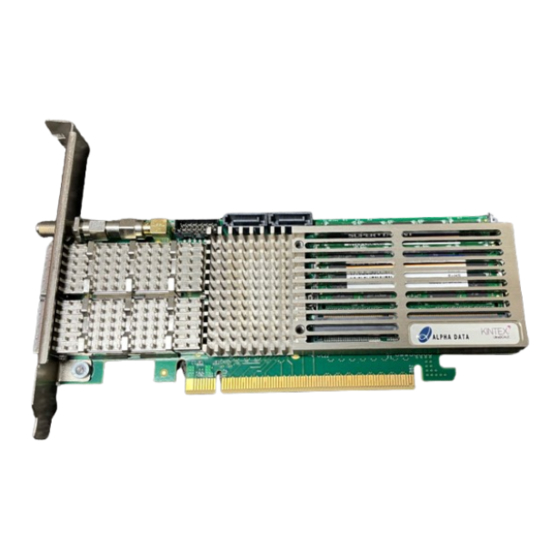
ADM-PCIE-KU3 User Manual 1 Introduction The ADM-PCIE-KU3 is a high-performance reconfigurable computing card intended for Data Center applications, featuring a Xilinx Kintex UltraScale FPGA. Figure 1 : ADM-PCIE-KU3 Product Photo 1.1 Key Features Key Features • PCIe Gen1/2/3 x1/2/4/8/16 capable (x16 requires bifurcation) •... -
Page 6: Pcb Information
The PCIe Specification permits a standard low-profile, half-length PCIe card to dissipate up to 25 W of power, drawn from the PCIe slot. The ADM-PCIE-KU3 may consume more than 25 W of power for larger user FPGA designs. Power estimation requires the use of the Xilinx XPE spreadsheet and/or a power estimator tool available from Alpha Data. -
Page 7: Thermal Performance
2.3 Thermal Performance The ADM-PCIE-KU3 comes with a heat sink to reduce the heat of the FPGA which is typically the hottest point on the card. The FPGA die temperature must remain under 100 degrees Celsius or the system monitor will clear the FPGA design to ensure the card does not overheat. -
Page 8: Functional Description
3 Functional Description 3.1 Overview The ADM-PCIE-KU3 is a versatile reconfigurable computing platform with a Kintex UltraScale KU040-2E FPGA, two Gen3x8 PCIe interface, two slots for DDR3-1600 SDRAM SODIMMs (64 bits with 8 bits ECC), two QSFP cages capable of 8x 10G or 2x 40G Ethernet, two SATA3 connectors, a SMA input for a timing synchronization input and a robust system monitor. -
Page 9: Switches
ADM-PCIE-KU3 User Manual 3.1.1 Switches The ADM-PCIE-KU3 has a quad DIP switch SW1, located on the rear side of the board in the middle of the card along the top edge. The function of each switch in SW1 is detailed below:... -
Page 10: Leds
ADM-PCIE-KU3 User Manual 3.1.2 LEDs There are 7 LEDs on the ADM-PCIE-KU3, 3 of which are general purpose and whose meaning can be defined by the user. The other four have fixed functions described below: DONE CLOCK_LOS SYS_Fault SYS_OK USR_LED0... -
Page 11: Clocking
ADM-PCIE-KU3 User Manual 3.2 Clocking The ADM-PCIE-KU3 provides reference clocks for the DDR3 SDRAM banks and the I/O interfaces available to the user. Any clock out of an Si5338 Clock Synthesizer is re-configurable over I2C. This allows the user to configure almost any arbitrary clock frequencies during application run time. -
Page 12: Fabric Clocks
ADM-PCIE-KU3 User Manual 3.2.2 Fabric Clocks The design offers 2 fabric clocks: REFCLK200M is a 200 MHz clock intended to be used for IDELAY elements in FPGA designs. REFCLK250M runs at 250 MHz and can be used to drive internal PLLs and other clocking resources. -
Page 13: Ddr3 Sdram Reference Clocks
The Both Si5338 clock generators are fully reconfigurable. The Alpha Data SDK provides API calls that re-configure certain frequencies with minimal effort. If a user is not using the Alpha Data SDK in their development, they can still change these frequencies manually over an I2C interface. Silicon labs provides detailed descriptions as to how this is done. -
Page 14: Pci Express
ADM-PCIE-KU3 User Manual 3.3 PCI Express The ADM-PCIE-KU3 is capable of PCIe Gen 1/2/3 with 1/2/4/8/16 lanes (where 16-lanes requires a two bifurcated 8-lane interfaces). The FPGA drives these lanes directly using the Integrated PCI Express block from Xilinx. Negotiation of PCIe link speed and number of lanes used is generally automatic and does not require user intervention. -
Page 15: Ddr3 Sdram Sodimms
ADM-PCIE-KU3 User Manual Signal Target FPGA Input P pin N pin PCIE_RX9 MGTHRX2_227 PCIE_TX10 MGTHTX1_227 PCIE_RX10 MGTHRX1_227 PCIE_TX11 MGTHTX0_227 PCIE_RX11 MGTHRX0_227 PCIE_TX12 MGTHTX3_226 PCIE_RX12 MGTHRX3_226 PCIE_TX13 MGTHTX2_226 PCIE_RX13 MGTHRX2_226 PCIE_TX14 MGTHTX1_226 PCIE_RX14 MGTHRX1_226 PCIE_TX15 MGTHTX0_226 PCIE_RX15 MGTHRX0_226 Table 11 : PCI Express Pin Assignments 3.4 DDR3 SDRAM SODIMMs... -
Page 16: Qsfp
ADM-PCIE-KU3 User Manual 3.5 QSFP Two QSFP cages are available at the front panel. Both cages are capable of housing either active optical or passive copper QSFP compatible components. The communication interface can run at up to 16.375Gbps per channel. There are eight channels between the two QSFP cages (total maximum bandwidth of 131Gbps). These cages are ideally suited for 8x 10G or 2x 40G Ethernet or any other protocol supported by the Xilinx GTH Transceivers. -
Page 17: Sata
Two SATA receptacles along the top of the board allow for internal chassis SATA management. The SATA interface can support the third generation SATA specification operating at 6 Gbps. Alpha Data can provide IP to manage the SATA devices connected at this interface. Please contact sales@alpha-data.com for more information regarding SATA IP. -
Page 18: System Monitor
A PC can directly interact with the TI Fusion IC via the PMBUS header in the design. This requires the following items: TI Fusion Communication Components • Programing Box: TI part number "USB-TO-GPIO" • TI Digital Power Designer software (http://www.ti.com/tool/fusion_digital_power_designer) • xml configuration file from Alpha Data (contact support@alpha-data.com) • Alpha-Data program adapter (contact sales@alpha-data.com) Page 14 Functional Description ad-ug-1284_v1_13.pdf... -
Page 19: Sma Timing Input
ADM-PCIE-KU3 User Manual 3.8 SMA Timing Input All cards are fitted with an SMA timing input at the front panel. This can be used to synchronize multiple cards within a system and to timestamp data. Input is on FPGA pin AG11, IOSTANDARD LVCMOS33 The signal is isolated through a optical isolator part number ACPL-M61L with a 1 Kohm resistor in series. -
Page 20: Jtag Front Panel Interface
JTAG connector on the PCB, a breakout cable can be purchased to bring this connection to the front panel. This item is sold separately. This item is intended to be used in conjunction with the Xilinx Platform Cable USB II. Alpha Data Part number: contact sales@alpha-data.com Figure 11 : JTAG cable from PCB to panel... -
Page 21: Configuration
ADM-XRC Gen 3 SDK, programmed into region 1 and "reg_access" into region 0. This permits basic confidence testing to be performed on a board without needing to program anything into the Flash memory. Alpha Data recommends that region 0 is never overwritten; this permits relatively simple recovery, without requiring a Xilinx Platform USB JTAG cable to be attached, in the event of programming a "bad"... -
Page 22: Building And Programming Configuration Images
ADM-PCIE-KU3 User Manual The Lockdown function of the Flash device is controlled via switch SW1-2. When SW1-2 is ON, any blocks in the Flash whose Lockdown flag is set are write-protected. The factory default for the Lockdown flag of all Flash blocks is clear, so that any block in the Flash can be written. -
Page 23: Table
ADM-PCIE-KU3 User Manual Revision History Date Revision Changed By Nature of Change Initial Release 15 Dec 2014 K. Roth Updated Product Photo, added section on SMA timing input, added section on JTAG front panel access, updated 17 Dec 2014 K. Roth description of user leds. - Page 24 ADM-PCIE-KU3 User Manual Page Intentionally left blank Address: 4 West Silvermills Lane Address: 611 Corporate Circle, Suite H Edinburgh, EH3 5BD, UK Golden, CO 80401 Telephone: +44 131 558 2600 Telephone: (303) 954 8768 Fax: +44 131 558 2700 Fax:...
Need help?
Do you have a question about the ADM-PCIE-KU3 and is the answer not in the manual?
Questions and answers