Table of Contents
Advertisement
Quick Links
Advertisement
Table of Contents

Related Manuals for Alpha Data FMC-CLINK-MINI


Summary of Contents for Alpha Data FMC-CLINK-MINI
- Page 1 FMC-CLINK-MINI User Manual Revision: V1.1...
- Page 2 FMC-CLINK-MINI User Manual © 2013 Copyright Alpha Data Parallel Systems Ltd. All rights reserved. This publication is protected by Copyright Law, with all rights reserved. No part of this publication may be reproduced, in any shape or form, without prior written consent from Alpha Data Parallel Systems Ltd.
-
Page 3: Table Of Contents
Base/Medium/Full Output Configuration .................. 12 Debug Pinout ..........................14 RS232 Electrical Specifications (J1) .................... 15 List of Tables Table 1 FMC-CLINK-MINI board features ...................... 2 Table 2 Configuration Switch Settings ......................3 Table 3 Camera Link Connector 1 (Dual Base Input Configuration) .............. 6 Table 4 Camera Link Connector 2 (Dual Base Input Configuration) .............. - Page 4 FMC-CLINK-MINI User Manual Page Intentionally left blank...
-
Page 5: Introduction
The FMC-CLINK-MINI provides support for 2 Base configuration inputs or one Medium or Full configuration input. In addition to being able to be used for image capture, the FMC-CLINK-MINI may also be used for emulation of either up to two Base format cameras or one Medium / Full format camera. -
Page 6: Specification
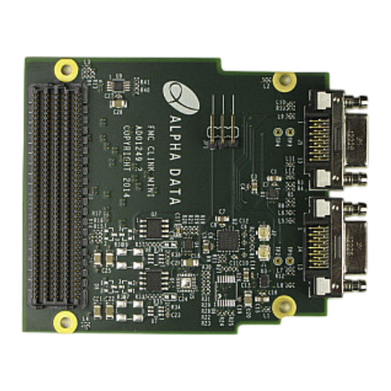
SDR cable assembly 3M part number 1SF26-L120-00C-XXX, where XXX= length in centimetres. SDR to MDR cable assembly 3M part number 1MF26-L560-00C-XXX, where XXX= length in centimetres. 2.3 Features Feature of the FMC-CLINK-MINI are shown below. Figure 2 : FMC-CLINK-MINI Feature Description... -
Page 7: Installation
User Manual 3 Installation The FMC-CLINK-MINI is designed to plug in to the FMC front panel connector on a compatible carrier. The retaining screws should be tightened to secure the FMC. Note:This operation should not be performed while the host PMC, XMC or PCI(e) card is powered up. -
Page 8: Order Code
FMC-CLINK-MINI User Manual 4 Order Code FMC-CLINK-MINI. For further information please contact Alpha Data. Page 4 Order Code ad-ug-1249_v1_1_FMC-CLink-MiniUserManual.pdf... -
Page 9: Design Examples
User Manual 5 Design Examples Example UCF, HDL files and Application software are available from Alpha Data for purchasers of this card when purchased with a compatible Alpha Data FPGA card. Available applications include a PCIe Camera Link Frame Grabber, and a PCIe Camera Link Emulator compatible with the ADPE-XRC-6T(-L). -
Page 10: Pinout
FMC-CLINK-MINI User Manual 6 Pinout 6.1 Camera Link Pinout Note: Some FMC pin have the N/P pairs swapped for particular configurations (signals marked with '*' in the tables below). These signals will need re-inverting in the connected FPGA. 6.1.1 Dual Base Input Configuration... -
Page 11: Camera Link Connector 2 (Dual Base Input Configuration)
FMC-CLINK-MINI User Manual Signal Name Direction FMC pin SDR pin (Con. 2) xclk_p LA_P_01 xclk_n LA_N_01 x_p<0> LA_P_06 x_n<0> LA_N_06 x_p<1> LA_P_07 x_n<1> LA_N_07 x_p<2> LA_P_08 x_n<2> LA_N_08 x_p<3> LA_P_09 x_n<3> LA_N_09 cc_p<1> LA_P_11 cc_n<1> LA_N_11 cc_p<2> LA_N_12* cc_n<2> LA_P_12* cc_p<3>... -
Page 12: Base/Medium/Full Input Configuration
FMC-CLINK-MINI User Manual 6.1.2 Base/Medium/Full Input Configuration Signal Name Direction FMC pin SDR pin (Con. 1) xclk_p LA_P_00 xclk_n LA_N_00 x_p<0> LA_P_02 x_n<0> LA_N_02 x_p<1> LA_P_03 x_n<1> LA_N_03 x_p<2> LA_P_04 x_n<2> LA_N_04 x_p<3> LA_P_05 x_n<3> LA_N_05 cc_p<1> LA_P_18 cc_n<1> LA_N_18 cc_p<2>... -
Page 13: Camera Link Connector 2 (Base/Medium/Full Input Configuration)
FMC-CLINK-MINI User Manual Signal Name Direction FMC pin SDR pin (Con. 2) yclk_p LA_P_01 yclk_n LA_N_01 y_p<0> LA_P_06 y_n<0> LA_N_06 y_p<1> LA_P_07 y_n<1> LA_N_07 y_p<2> LA_P_08 y_n<2> LA_N_08 y_p<3> LA_P_09 y_n<3> LA_N_09 zclk_p LA_P_17 zclk_n LA_N_17 z_p<0> LA_P_10 z_n<0> LA_N_10 z_p<1>... -
Page 14: Dual Base Output Configuration
FMC-CLINK-MINI User Manual 6.1.3 Dual Base Output Configuration Signal Name Direction FMC pin SDR pin (Con. 1) xclk_p LA_N_18* xclk_n LA_P_18* x_p<0> LA_P_21 x_n<0> LA_N_21 x_p<1> LA_N_20* x_n<1> LA_P_20* x_p<2> LA_P_19 x_n<2> LA_N_19 x_p<3> LA_N_14* x_n<3> LA_P_14* cc_p<1> LA_N_00* cc_n<1>... -
Page 15: Camera Link Connector 2 (Dual Base Output Configuration)
FMC-CLINK-MINI User Manual Signal Name Direction FMC pin SDR pin (Con. 2) xclk_p LA_N_11* xclk_n LA_P_11* x_p<0> LA_N_13* x_n<0> LA_P_13* x_p<1> LA_N_17* x_n<1> LA_P_17* x_p<2> LA_N_12* x_n<2> LA_P_12* x_p<3> LA_N_10* x_n<3> LA_P_10* cc_p<1> LA_N_01* cc_n<1> LA_P_01* cc_p<2> LA_P_08 cc_n<2> LA_N_08 cc_p<3>... -
Page 16: Base/Medium/Full Output Configuration
FMC-CLINK-MINI User Manual 6.1.4 Base/Medium/Full Output Configuration Signal Name Direction FMC pin SDR pin (Con. 1) xclk_p LA_N_18* xclk_n LA_P_18* x_p<0> LA_P_21 x_n<0> LA_N_21 x_p<1> LA_N_20* x_n<1> LA_P_20* x_p<2> LA_P_19 x_n<2> LA_N_19 x_p<3> LA_N_14* x_n<3> LA_P_14* cc_p<1> LA_N_00* cc_n<1> LA_P_00* cc_p<2>... -
Page 17: Table
FMC-CLINK-MINI User Manual Signal Name Direction FMC pin SDR pin (Con. 2) yclk_p LA_N_11* yclk_n LA_P_11* y_p<0> LA_N_13* y_n<0> LA_P_13* y_p<1> LA_N_17* y_n<1> LA_P_17* y_p<2> LA_N_12* y_n<2> LA_P_12* y_p<3> LA_N_10* y_n<3> LA_P_10* zclk_p LA_N_07* zclk_n LA_P_07* z_p<0> LA_N_09* z_n<0> LA_P_09* z_p<1>... -
Page 18: Debug Pinout
FMC-CLINK-MINI User Manual 6.2 Debug Pinout Signal Name Direction FMC pin Notes Drive high to led<0> LA_P_25 illuminate Drive high to led<1> LA_P_26 illuminate Drive high to led<2> LA_P_27 illuminate Drive high to led<3> LA_P_28 illuminate Table 11 : LED Indicators... -
Page 19: Rs232 Electrical Specifications (J1)
FMC-CLINK-MINI User Manual 7 RS232 Electrical Specifications (J1) The tables below show the electrical characteristics of the RS232 connection under typical operating conditions. RX Inputs Units Input Voltage Range Input Threshold Low Input Threshold High Input Hysteresis kΩ Input Resistance... - Page 20 FMC-CLINK-MINI User Manual Page 16 RS232 Electrical Specifications (J1) ad-ug-1249_v1_1_FMC-CLink-MiniUserManual.pdf...
- Page 21 FMC-CLINK-MINI User Manual Revision History Date Revision Nature of Change 14th Sept. 2012 Initial Release Correct SDR pins in Camera Link Connector 2 (Base/ 5th Aug. 2013 Medium/Full Input Configuration) RS232 Electrical Specifications (J1) Page 17 ad-ug-1249_v1_1_FMC-CLink-MiniUserManual.pdf...
- Page 22 FMC-CLINK-MINI User Manual Page Intentionally left blank Address: 4 West Silvermills Lane, Address: 3507 Ringsby Court Suite 105, Edinburgh, EH3 5BD, UK Denver, CO 80216 Telephone: +44 131 558 2600 Telephone: (303) 954 8768 Fax: +44 131 558 2700 Fax:...
Need help?
Do you have a question about the FMC-CLINK-MINI and is the answer not in the manual?
Questions and answers