Table of Contents
Advertisement
Quick Links
UM1842
User manual
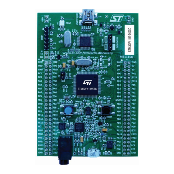
Discovery kit with STM32F411VE MCU
Introduction
The STM32F411 Discovery kit (32F411EDISCOVERY) helps you to discover the entry level
of the STM32F4 series and to develop your applications. It is based on an
STM32F411VET6 microcontroller and includes an ST-LINK/V2 embedded debug tool
interface, ST MEMS Gyroscope, ST MEMS accelerometer + magnetometer, ST MEMS
digital microphone, audio DAC with integrated class D speaker driver, LEDs, pushbuttons
and a USB OTG micro-AB connector.
Figure 1. STM32F411 Discovery board
December 2014
DocID027213 Rev 1
1/35
1
www.st.com
Advertisement
Table of Contents

Related Manuals for ST STM32F411


Summary of Contents for ST STM32F411
- Page 1 Discovery kit with STM32F411VE MCU Introduction The STM32F411 Discovery kit (32F411EDISCOVERY) helps you to discover the entry level of the STM32F4 series and to develop your applications. It is based on an STM32F411VET6 microcontroller and includes an ST-LINK/V2 embedded debug tool...
-
Page 2: Table Of Contents
Embedded ST-LINK/V2 ........ - Page 3 UM1842 Contents Revision history ......... . . 34 DocID027213 Rev 1 3/35...
- Page 4 List of tables UM1842 List of tables Table 1. ON/OFF conventions ............6 Table 2.
- Page 5 Figure 6. STM32F411 Discovery board connections image ....... 13 Figure 7.
-
Page 6: Conventions
Conventions UM1842 Conventions provides the definition of some conventions used in the present document. Table 1 Table 1. ON/OFF conventions Convention Definition Jumper JPx ON Jumper fitted Jumper JPx OFF Jumper not fitted Solder bridge SBx ON SBx connections closed by solder Solder bridge SBx OFF SBx connections left open 6/35... -
Page 7: Quick Start
Ensure that the jumpers JP2 and CN3 are set to "on" (Discovery mode). Connect the STM32F411 Discovery board to a PC using a USB cable type A/mini-B through the USB ST-LINK connector CN1, to power the board. The LED LD2 (PWR) will light up and the four LEDs between the buttons B1 and B2 start blinking. -
Page 8: Features
STM32F411VET6 microcontroller featuring 512 KB of Flash memory, 128 KB of RAM in an LQFP100 package On-board ST-LINK/V2 with selection mode switch to use the kit as a standalone ST- LINK/V2 (with SWD connector for programming and debugging) ... -
Page 9: Hardware Layout
UM1842 Hardware layout Hardware layout The STM32F411 Discovery board has been designed around the STM32F411VET6 microcontroller in a 100-pin LQFP package. illustrates the connections between the STM32F411VET6 and its peripherals (ST- Figure 2 LINK/V2, pushbutton, LED, Audio DAC, USB, ST MEMS gyroscope, ST MEMS accelerometer + magnetometer, ST MEMS microphone, and connectors). -
Page 10: Figure 3. Top Layout
Hardware layout UM1842 Figure 3. Top layout 10/35 DocID027213 Rev 1... -
Page 11: Figure 4. Bottom Layout
UM1842 Hardware layout Figure 4. Bottom layout DocID027213 Rev 1 11/35... -
Page 12: Embedded St-Link/V2
Hardware layout UM1842 Embedded ST-LINK/V2 The ST-LINK/V2 programming and debugging tool is integrated on the STM32F411 Discovery board. The embedded ST-LINK/V2 can be used in 2 different ways according to the jumper states (see Table Program/debug the MCU on board, ... -
Page 13: Using St-Link/V2 To Program/Debug The Stm32F411 On Board
Using ST-LINK/V2 to program/debug the STM32F411 on board To program the STM32F411 on board, simply plug in the two jumpers on CN3, as shown in in red, but do not use the CN2 connector as that could disturb communication with Figure 6 the STM32F411VET6 of the STM32F411 Discovery board. -
Page 14: Using St-Link/V2 To Program/Debug An External Stm32 Application
4.1.2 Using ST-LINK/V2 to program/debug an external STM32 application It is very easy to use the ST-LINK/V2 to program the STM32 on an external application. Simply remove the 2 jumpers from CN3 as shown in 7, and connect your application... -
Page 15: Power Supply And Power Selection
5 V can also be used as input power supplies, e.g. when the USB connector is not connected to the PC. In this case, the STM32F411 Discovery board must be powered by a power supply unit or by an auxiliary equipment complying with standard EN-60950-1: 2006+A11/2009, and must be Safety Extra Low Voltage (SELV) with limited power capability. -
Page 16: On Board Audio Capability
CS43L22 USB OTG supported The STM32F411 is used to drive only USB OTG full speed on this board. The USB micro- AB connector (CN5) allows the user to connect a host or device component, such as a USB key, mouse, and so on. -
Page 17: Jp2 (Idd)
If PH0 and PH1 are only used as GPIOs instead of as a clock, then SB14 and SB16 are closed and R24, R25 and R66 are removed. MCO from ST-LINK (from MCO of the STM32F103) This frequency cannot be changed, it is fixed at 8 MHz and connected to PH0-OSC_IN of the STM32F411VET6. -
Page 18: Boot0 Configuration
SWO signal of the CN2 connector is connected to PB3 SB15 (SWO) SWO signal is not connected Reserved, do not modify SB10,11 (RX,TX) Reserved, do not modify No incidence on STM32F103C8T6 (ST-LINK/V2) NRST signal SB12 (STM_RST) STM32F103C8T6 (ST-LINK/V2) NRST signal is connected to GND 18/35 DocID027213 Rev 1... -
Page 19: Extension Connectors
4.13 Extension connectors The male headers P1 and P2 can connect the STM32F411 Discovery board to a standard prototyping/wrapping board. STM32F411VET6 GPI/Os are available on these connectors. P1 and P2 can also be probed by an oscilloscope, logical analyzer or voltmeter. - Page 20 Hardware layout UM1842 Table 5. MCU pin description versus board function (page 2 of 8) (continued) MCU pin Board function Main Alternate function functions SPI1_NSS, SPI3_NSS/I2S3_WS, USART2_CK, ADC1_4 TIM2_CH1/TIM2_ETR, SPI1_SCK, ADC1_5 TIM1_BKIN, TIM3_CH1, SPI1_MISO, ADC1_6 TIM1_CH1N, TIM3_CH2, SPI1_MOSI, ADC1_7 MCO_1, TIM1_CH1, I2C3_SCL, USART1_CK, USB_FS_SOF...
- Page 21 UM1842 Hardware layout Table 5. MCU pin description versus board function (page 3 of 8) (continued) MCU pin Board function Main Alternate function functions PA13 JTMS-SWDIO JTCK-SWCLK, PA14 I2S3ext_WS JTDI, TIM2_CH1/TIM2_ETR, PA15 SPI1_NSS, SPI3_NSS/I2S3_WS TIM1_CH2N, TIM3_CH3, ADC1_8 TIM1_CH3N, TIM3_CH4, ADC1_9 JTDO-SWO, TIM2_CH2, SPI1_SCK, SPI3_SCK/I2S3_CK,...
- Page 22 Hardware layout UM1842 Table 5. MCU pin description versus board function (page 4 of 8) (continued) MCU pin Board function Main Alternate function functions TIM4_CH3, TIM10_CH1, I2C1_SCL, USB_FS_SCL, SDIO_D4 TIM4_CH4, TIM11_CH1, I2C1_SDA, SPI2_NSS/I2S2_WS, USB_FS_SDA, SDIO_D5 TIM2_CH3, I2C2_SCL, PB10 SPI2_SCK/I2S2_CK VCAP1 TIM1_BKIN, I2C2_SMBAL, PB12...
- Page 23 UM1842 Hardware layout Table 5. MCU pin description versus board function (page 5 of 8) (continued) MCU pin Board function Main Alternate function functions SPI2_MOSI/I2S2_SD, ADC1_13 ADC1_14 ADC1_15 TIM3_CH1, I2S2_MCK, USART6_TX, SDIO_D6 TIM3_CH2, I2S3_MCK, USART6_RX, SDIO_D7 MCO_CPUCK, TIM3_CH3, USART6_CK, SDIO_D0 MCO_2, TIM3_CH4, I2C3_SDA, I2S2_CKIN, SDIO_D1...
- Page 24 Hardware layout UM1842 Table 5. MCU pin description versus board function (page 6 of 8) (continued) MCU pin Board function Main Alternate function functions PD10 PD11 PD12 TIM4_CH1 PD13 TIM4_CH2 PD14 TIM4_CH3 PD15 TIM4_CH4 TIM4_ETR 24/35 DocID027213 Rev 1...
- Page 25 UM1842 Hardware layout Table 5. MCU pin description versus board function (page 7 of 8) (continued) MCU pin Board function Main Alternate function functions PE10 PE11 TIM1_CH2, SPI4_NSS TIM1_CH3N, PE12 SPI4_SCK PE13 TIM1_CH3, SPI4_MISO 44 PE14 TIM1_CH4, SPI4_MOSI 45 PE15 TIM1_BKIN OSC_IN OSC_OUT...
- Page 26 Hardware layout UM1842 Table 5. MCU pin description versus board function (page 8 of 8) (continued) MCU pin Board function Main Alternate function functions 1. The default configuration for the functions used on the boards, is shown in grey color. 26/35 DocID027213 Rev 1...
-
Page 27: Mechanical Drawing
UM1842 Mechanical drawing Mechanical drawing Figure 8. STM32F411 Discovery board mechanical drawing DocID027213 Rev 1 27/35... -
Page 28: Electrical Schematics
Electrical schematics Figure 9. STM32F411 Discovery board ST_LINK_V2.SCHDOC U_ST_LINK U_STM32Fx U_Audio STM32Fx.SchDoc Audio.SchDoc PB10 PB10 STM32F4_USART2_TX PA14 TCK/SWCLK PC12 PA14 PC12 STM32F4_USART2_RX PA13 TMS/SWDIO PC10 PA13 PC10 NRST T_NRST NRST T_SWO U_IO Peripherals IO Peripherals.SchDoc U_USB_OTG_FS PA10 PE10 PD12 PA10... -
Page 29: Figure 10. St-Link/V2 (Swd Only)
Figure 10. ST-LINK/V2 (SWD only) TCK/SWCLK PA14 TMS/SWDIO PA13 T_NRST NRST T_SWO SB13 SB15 100K Board Ident: PC13=0 [NA] AIN_1 [NA] BAT60JFILM T_JTCK SWCLK STM32F103C8T6 STM_JTCK T_JTMS SWDIO 20pF 20pF T_NRST STM_JTMS VBAT VDD_2 Header 6 PC13 VSS_2 STM_JTMS T_SWO... -
Page 30: Figure 11. Stm32F411Vet6 Mcu
Figure 11. STM32F411VET6 MCU BOOT1 PA10 PE10 PA10 PA10 PE10 PE10 PA11 PE11 PA11 PA11 PE11 PE11 PA12 PE12 PA12 PA12 PE12 PE12 PA13 PE13 PA13 PA13 PE13 PE13 PA14 PE14 PA14 PA14 PE14 PE14 PA15 PE15 PA15 PA15 PE15 PE15 SB20 Must be close to the Crystal... -
Page 31: Figure 12. Audio
Figure 12. Audio 22nF 22nF Audio_SDA HP/LINE_OUTA Audio_SCL HP/LINE_OUTB SPKR/HP I2S3_MCK ST-225-02 MCLK I2S3_SCK PC10 PC10 SCLK SPKR_OUTA+ I2S3_SD PC12 PC12 SDIN SPKR_OUTA- I2S3_WS LRCK SPKR_OUTB+ Audio_RST RESET SPKR_OUTB- 100nF 100nF -VHPFILT FLYN AIN1B Audio_DAC_OUT AIN1A [NA] FLYP AIN2B AIN2A... -
Page 32: Figure 13. Usb_Otg_Fs
Figure 13. USB_OTG_FS LED, red OTG_FS_OverCurrent FAULT OTG_FS_PowerSwitchOn VBUS STMPS2141STR 4.7uF Shield VBUS_FS USB-MICRO-AB OTG_FS_DM PA11 PA11 OTG_FS_DP PA12 PA12 OTG_FS_ID PA10 PA10 Vbus D+out D+in D-out D-in LED, green EMIF02-USB03F2 9013-SOT23 [NA] Title: STM32F411E-DISCOVERY USB_OTG_FS Number: MB1115 Rev: B.2(PCB.SCH) Date: 10/16/2014 Sheet... -
Page 33: Figure 14. Peripherals
Figure 14. Peripherals [NA] NRST NRST [NA] SB21 100nF 220K USER & WAKE-UP Button RESET Button 10uF VDD_IO 220nF SETC PD12 SETP PD12 INT2 LED, green INT1 DRDY 100nF PD13 PD13 LED, orange LSM303DLHC 4.7uF PD14 PD14 LED, red PD15 PD15 LED, blue VDD_IO... -
Page 34: Table 6. Document Revision History
Revision history UM1842 Revision history Table 6. Document revision history Date Revision Changes 16-Dec-2014 Initial release. 34/35 DocID027213 Rev 1... - Page 35 ST products and/or to this document at any time without notice. Purchasers should obtain the latest relevant information on ST products before placing orders. ST products are sold pursuant to ST’s terms and conditions of sale in place at the time of order acknowledgement.
Need help?
Do you have a question about the STM32F411 and is the answer not in the manual?
Questions and answers