Table of Contents
Advertisement
Quick Links
Advertisement
Table of Contents

Related Manuals for Thundercomm TurboX C865 Dev Kit


Summary of Contents for Thundercomm TurboX C865 Dev Kit
- Page 1 TurboX C865 Dev Kit Hardware User Guide Rev. A June 06, 2020...
- Page 2 Revision history Revision Date Description May 26, 2020 Initial Release June 06, 2020 Delete box content description `www.thundercomm.com.
-
Page 3: Table Of Contents
Contents TurboX C865 Dev Kit ............................8 TurboX C865 Dev Kit Key Features ....................8 Board views ............................10 1.2.1 Top view ............................ 10 1.2.2 Back view ..........................10 Terms and Definitions .........................11 Start the board ..............................12 Required equipment ........................... 12 OS startup process .......................... - Page 4 I2C ............................. 25 4.1.3 GPIO ............................25 4.1.4 SPI.............................. 25 4.1.5 PCM/I2S ............................ 26 4.1.6 Power and Reset......................... 26 4.1.7 Power Supplies .......................... 26 Secondary Low Speed Connector: LS2 ..................... 27 4.2.1 Audio ............................29 4.2.2 Stereo speaker ..........................29 `www.thundercomm.com.
- Page 5 5.1.8 USB............................40 Secondary High Speed Connector: HS2 .................... 40 5.2.1 MIPI CSI ............................ 43 5.2.2 Clock ............................43 5.2.3 SPI.............................. 43 5.2.4 PCIe1 ............................43 5.2.5 USB............................44 5.2.6 Other signals on Secondary High Speed Connector ..............44 `www.thundercomm.com.
- Page 6 Reset Button ..........................51 7.1.5 Force_USB_BOOT button ......................52 LED’s ..............................52 7.2.1 User LED 1-4 ..........................52 7.2.2 Wi-Fi status ..........................52 7.2.3 Bluetooth status.......................... 52 7.2.4 Power Indicator LED ......................... 52 Boot configuration ............................. 53 Mechanical specification ........................... 54 `www.thundercomm.com.
- Page 7 Navigation Mezzanine ........................57 10.1.1 Technical specifications ......................57 10.1.2 Board views ..........................58 Top view ..............................58 Bottom view............................... 58 10.2 Machine Communication Mezzanine ....................59 10.2.1 Technical specifications ......................59 10.2.2 Board views ..........................60 Top view ..............................60 `www.thundercomm.com.
-
Page 8: Turbox C865 Dev Kit
1 TurboX C865 Dev Kit TurboX C865 Dev Kit is comprised of an extensive set of hardware, software and development tools. And it is the first of its kind to bring together the Qualcomm’s deep expertise in 5G and AI to empower developers and manufacturers to create the next generation of high-compute, low-power robots and drones for the consumer, enterprise, defense, industrial and professional service sectors –... - Page 9 Operation Temperature: -20℃ ~ 70℃ Operating Environment Operation Humidity: 5%~95%, non-condensing 12V@2.5A adapter with a DC plug, with inner diameter as 1.75mm and outer Power supply diameter as 4.75mm 85mm x 54mm, meeting 96Boards Consumer Edition Standard form dimensions Dimension specifications `www.thundercomm.com.
-
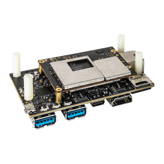
Page 10: Board Views
1.2 Board views (C865 Main IO board) 1.2.1 Top view 1.2.2 Back view `www.thundercomm.com. -
Page 11: Terms And Definitions
1.3 Terms and Definitions Component Description Qualcomm Universal Peripheral The QUP engine provides a general-purpose data path that supports multiple mini cores, e.g., UART, I2C and SPI Camera Control Interface SPMI System Power Management Interface `www.thundercomm.com. -
Page 12: Start The Board
2 Start the board 2.1 Required equipment Equipment Description C865 SOM based on the Qualcomm® SM8250 processor TurboX C865 DEV KIT C865 Main IO board based on 96board requirement development board Power adapter 12 V with 2500 mA required per 96Boards specification USB to Micro USB ... - Page 13 6. Plug the power supply into a power outlet. 7. Press, and hold the power button on the device, and then release it. The green power-up LED should illuminate in a second. 8. The board will start the booting process. `www.thundercomm.com.
-
Page 14: Turbox C865 Dev Kit
TurboX C865 Dev Kit 3.1 System Block diagram Block diagram part#1 Block diagram part#2 `www.thundercomm.com. -
Page 15: Processor
The LPDDR5 interface goes directly to the SM8250 built-in LPDDR controller. The maximum DDR clock is 2750MHz. The UFS flash memory interfaces with SM8250 over a dedicated UFS PHY bus supporting the UFS 3.0 specification. 3.4 MicroSD MicroSD slot signals are routed directly to the SM8250 SDC2 interface. `www.thundercomm.com. -
Page 16: Wi-Fi/Bt
DCS 1.02.00), an I2C channel from the SM8250 also allows users to configure the operation of this bridge. It is QUP5 I2C interface from SoC. This bridge supports audio as well (meeting the 96Boards requirements for providing audio via HDMI). The `www.thundercomm.com. -
Page 17: Mipi-Dsi
4-lane CSI2 camera on high-speed connector HS2 (section1.2.1 #13) 4-lane CSI3 camera on high-speed connector HS1 (section1.2.1 #6) and high-speed connector (section1.2.1 #7) 4-lane CSI4 camera on high-speed connector HS3 (section1.2.1 #7) 4-lane CSI5 camera on high-speed connector HS3 (section1.2.1 #7) 3.8 USB Ports `www.thundercomm.com. -
Page 18: Usb-Host Ports
The BT 5.1 implementation (including audio) on the C865 DEV KIT is with SM8250 and QCA6391. 3.9.2 HDMI Audio A 4-bit (audio out only) I2S channel is routed directly from the SM8250 SoC I2S interface pins to the DSI-HDMI bridge. 3.9.3 DisplayPort Audio `www.thundercomm.com. -
Page 19: Dc-Power And Battery Power
The 4bit UART comes directly from SoC pins to low-speed expansion connector. The 2bit UART is optional an on-board UART debug log port via Micro USB port#21, or to be routed to low-speed expansion connector. To use the port for log output, switch DIP_DEBUG_UART_SWITCH on DIP switch (section 1.2.2#16) to ON. 3.15 JTAG (NA) `www.thundercomm.com. -
Page 20: System And User Leds
No impact to the physical footprint specification (including height) No impact to the use of 96Boards CE low-speed and high-speed expansion facilities C865 DEV KIT implements a few additional functions as described from Sections 3.17.1 to 3.17.4 3.18.1 Ethernet Connector `www.thundercomm.com. -
Page 21: Inertial Sensors
Switch 6 – IMU_EXT_CLK_TOGGLE: When set to ON, the onboard ICM-42688 sensor will use the external CLK of GPIO3 from PM8250; when set to OFF, the onboard ICM-42688 sensor will output interrupt to SoC GPIO113. These GPIOs need the software configure setting. `www.thundercomm.com. -
Page 22: Extra Low Speed Expansion Connector
3.18.4 Extra Low Speed Expansion Connector C865 DEV KIT has 3 extra low-speed expansion connectors. See Section 4 for detail. 3.18.5 Extra High Speed Expansion Connectors C865 DEV KIT has 3 high-speed expansion connector. See Section 5 for detail `www.thundercomm.com. -
Page 23: Low Speed Expansion Connector
QUP13 UART0_TXD QUP13 UART0_RXD QUP13 UART0_RTS QUP13 UART1_TXD QUP12 UART1_RXD QUP12 I2C0_SCL QUP4 I2C0_SDA QUP4 I2C1_SCL QUP15 I2C1_SDA QUP15 GPIO-A/QUP-A0 QUP1 GPIO-C/QUP-A1 QUP1 GPIO-E/QUP-A2 QUP1 GPIO-G DISPLAY_VSYNC GPIO-I CAM0_RST_N GPIO-K CAM1_RST_N +1V8 From PM8250 BUCK From on board DCDC `www.thundercomm.com. -
Page 24: Uart
The 96Boards specification calls for a 4-wire UART implementation, UART0 and an optional second 2-wire UART, UART1 on the low-speed expansion connector. C865 DEV KIT implements UART0 as a 4-wire UART that connects directly to the SM8250 SoC. These signals are driven at 1.8 V. `www.thundercomm.com. -
Page 25: I2C
GPIO J: Connects to GPIO_114 of SM8250 SoC. GPIO K: Connects to GPIO_92 of SM8250 SoC. GPIO L: Connects to GPIO_109 of SM8250 SoC. 4.1.4 SPI The 96Boards specification calls for one SPI bus master to be provided on the low-speed expansion connector. `www.thundercomm.com. -
Page 26: Pcm/I2S
C865 DEV KIT supports these requirements as follows: +1.8 V: Driven by PMIC PM8250 VREG_S4A_1P8, which can provide 100mA. +5 V: Driven by the 4A 5.0 V DC to DC converter. The buck can provide at least current of 2A to `www.thundercomm.com. -
Page 27: Secondary Low Speed Connector: Ls2
4.2 Secondary Low Speed Connector: LS2 C865 Dev Kit Signal Additional Info GPIO_U CAM3_RST_N DMIC_CLK1_LS2 DMIC_DATA1_LS2 GPIO_V I2S1_DATA2/ext codec/CAM0_STROBE_N DMIC_CLK2 DMIC_DATA2 GPIO_W I2S1_DATA3/ext codec/CAM5_RST_N DMIC_CLK3 DMIC_DATA3 PM_GPIO-F PM8250_GPIO3 CCI_I2C_SCL2 CCI_I2C_SDA2 CCI_I2C_SCL3 SPK0_P SPK0_M SPK1_P SPK1_M CCI_I2C_SDA3 PM_GPIO-E PM8250 AMUX1/MDM SKIN THERM `www.thundercomm.com. - Page 28 Additional Info GPIO_Z CAM4_RST_N CAN_H CAN_L VREG_IO_1P8 PM_GPIO-A PM8150L GPIO6 PM_GPIO-B PM8150L GPIO10 GPIO-M/QUP-B0 QUP9 GPIO-N/QUP-B1 QUP9 GPIO-O/QUP-B2 QUP9/PWM GPIO-P/QUP-B3 QUP9/BOOT_CONFIG 0 GPIO-Q GPIO 147 GPIO-R GPIO 148 GPIO-S GPIO 148 GPIO-T GPIO 149 PM_AMUX1 PM8150L PM_AMUX2 PM8150L BATT_THERM BATT_ID `www.thundercomm.com.
-
Page 29: Audio
4.2.3 Digital Microphones The expansion connector supports 3 additional default digital microphone inputs, support maximum 6 DMICs: DMIC_CLK1_LS2 DMIC_DATA1_LS2 DMIC_CLK1/DATA1_LS2 are multiplexing with on board MIC, see Section 3.18.3, switch1 of DIP switch#16 DMIC_CLK2 DMIC_DATA2 `www.thundercomm.com. -
Page 30: Can
GPIO-M/QUP-B0: Connects to GPIO_125 of SM8250. GPIO-N/QUP-B1: Connects to GPIO_126 of SM8250. GPIO-O/QUP-B2: Connects to GPIO_127 of SM8250. GPIO-P/QUP-B3: Connects to GPIO_128 of SM8250. GPIO-Q/I2S1_WS_LS2: Connects to GPIO_147 of SM8250. Can be configured as I2S WS `www.thundercomm.com. -
Page 31: Other Signals On Secondary Low Speed Connector
USB_VBUS : Connects to VBUS of PM8250 PMIC, Can be configured as an OTG USB VBUS. VBAT : Connects to a DC-DC buck of board power, be configured as output 4.2V source. 4.3 Tertiary Low Speed Connector: LS3 C865 Dev Kit Signal Additional Info GPIO-KK CAM2_STROBE SLEEP_CLK GPIO-LL CAM3_STROBE GPIO-MM QUP19 `www.thundercomm.com. - Page 32 SPI2_CS1 SSC QUP2 SPI3_CS1 SSC QUP5 VREG_L8C_1P8 VDC_5V A board DC buck power 5V VBAT A board DC buck power 4.2V GPIO-RR QUP18 GPIO-SS SSC QUP4/I2C SDA C865 Dev Kit Signal Note GPIO-TT CAM4_STROBE PMK8002_PMIC_CLK GPIO-UU CAM5_STROBE/WCD_RESET QCA_GPIO-D DISP_RST_N `www.thundercomm.com.
-
Page 33: Ssc Spi
SPI2_CLK_LS3: Connects to SSC QUP2 of SM8250 SoC, to be configured to CLK. SPI2_MOSI_LS3: Connects to SSC QUP2 of SM8250 SoC, to be configured to MOSI. SPI2_MISO_LS3: Connects to SSC QUP2 of SM8250 SoC, to be configured to MISO. `www.thundercomm.com. -
Page 34: Ssc I2C
4.3.4 Other signals on Tertiary Low Speed Connector The C865 DEV KIT board implements more source voltage at the Lowe Speed Expansion Connector. The signals are: VREG_L5C_1P8: Connects to L5 LDO of PM8250 PMIC, Can be as sensor IO voltage source. `www.thundercomm.com. - Page 35 VREG_L8C_1P8: Connects to L8 LDO of PM8250 PMIC, Can be as sensor IO voltage source. VDC_5V: Connects to a board DC buck power 5V, Can be as a 5V voltage source. VBAT: Connects to a board DC buck power 4.2V, Can be as a 4.2V voltage source. `www.thundercomm.com.
-
Page 36: High Speed Expansion Connectors
5.1 Primary high speed expansion connector: HS1 The following table shows the High Speed Expansion Connector pin out: 96Boards Signals Note SD_DAT0 SDC4_DATA0 SD_DAT1 SDC4_DATA1 SD_DAT2 SDC4_DATA2 SD_DAT3 SDC4_DATA4 SD_SCLK SDC4_SCLK SD_CMD SDC4_CMD CLK0/CSI0_MCLK CLK3/CSI3_MCLK DSI0_CLK_P_HS1 DSI0_CLK_M_HS1 DSI0_D0_P_HS1 DSI0_D0_M_HS1 DSI0_D1_P_HS1 DSI0_D1_M_HS1 DSI0_D2_P_HS1 `www.thundercomm.com. - Page 37 DSI0_D2_M_HS1 DSI0_D3_P_HS1 DSI0_D3_M_HS1 USB1_HS_DP_HS1 USB1_HS_DM_HS1 C865 Dev Kit Signals Note CSI0_C_P CSI0_C_M CSI0_D0_P CSI0_D0_M CSI0_D1_P CSI0_D1_M CSI0_D2_P CSI0_D2_M `www.thundercomm.com.
-
Page 38: Mipi Dsi
CSI0_D3_P CSI0_D3_M CCI_I2C_SCL0 CCI_I2C_SDA0 CCI_I2C_SCL1 CCI_I2C_SDA1 CSI3_D0_P CSI3_D0_M CSI3_D1_P CSI3_D1_M CSI3_C_P CSI3_C_M RESERVED Can be pull-up to 1.8V by adding a serial resistor. 5.1.1 MIPI DSI `www.thundercomm.com. -
Page 39: Mipi Csi
NOTE: Both interfaces, I2C0 and I2C1 are pull-up to 1.8V via 2.2K resistor in 865SOM. 5.1.4 HSIC The 96Boards specification calls for an optional MIPI-HSIC interface to be present on the High Speed Expansion Connector. The C865 DEV KIT board implementation doesn’t support this optional requirement. `www.thundercomm.com. -
Page 40: Reserved
The 96Boards specification calls for a USB data line interface to be present on the high-speed expansion connector. C865 DEV KIT implements this requirement. In HS1, USB HS DP/DM signals are routing from a USB HUB. 5.2 Secondary High Speed Connector: HS2 C865 DEV KIT Signals Note PCIE_REFCLK_M PCIE_REFCLK_P PCIE_RX_M PCIE_RX_P `www.thundercomm.com. - Page 41 PCIE_TX_M PCIE_TX_P GPIO-CC PCIE1_RST_N GPIO-DD PCIE1_CLK_REQ_N GPIO-EE PCIE1_WAKE_N GPIO-FF PCIE2_RST_N GPIO-GG PCIE2_CLK_REQ_N GPIO-HH PCIE2_WAKE_N CLK1/CSI1_MCLK CLK2/CSI2_MCLK CSI2_C_P CSI2_C_M CSI2_D0_P CSI2_D0_M CSI2_D1_P CSI2_D1_M CSI2_D2_P CSI2_D2_M CSI2_D3_P CSI2_D3_M `www.thundercomm.com.
- Page 42 C865 DEV KIT Signals Note CSI1_C_P CSI1_C_M CSI1_D0_P CSI1_D0_M CSI1_D1_P CSI1_D1_M CSI1_D2_P CSI1_D2_M CSI1_D3_P CSI1_D3_M SPI1_CLK QUP14 SPI1_CS QUP14 SPI1_MOSI QUP14 SPI1_MISO QUP14 CLK4/CSI4_MCLK CLK5/CSI5_MCLK GPIO-II CAM2_RST_N GPIO-JJ CAM2_PWDN PMIC_SPMI_CLK `www.thundercomm.com.
-
Page 43: Mipi Csi
: Connects to QUP 14 of SM8250 SoC. Be configured to MOSI. SPI1_MISO : Connects to QUP 14 of SM8250 SoC. Be configured to MISO. 5.2.4 PCIe1 The C865 DEV KIT has 2 2-lane PCIe interfaces. PCIe1 1-lane is available on the Secondary High Speed Expansion Connector. `www.thundercomm.com. -
Page 44: Usb
GPIO-II: Connects to GPIO_78 of SM8250 SoC. Can be configured as Camera2 Reset. GPIO-JJ: Connects to GPIO_47 of SM8250 SoC. Can be configured as Camera2 power down, QUP 14 CS or BOOT CONFIG 2. PMIC_SPMI_CLK: Can be connected to SDX55 module. PMIC_SPMI_DATA: Can be connected to SDX55 module. `www.thundercomm.com. -
Page 45: Tertiary High Speed Connector: Hs3
5.3 Tertiary High Speed Connector: HS3 C865 DEV KIT Signals Note CSI4_C_P CSI4_C_M CSI4_D0_P CSI4_D0_M CSI4_D1_P CSI4_D1_M CSI4_D2_P CSI4_D2_M CSI4_D3_P CSI4_D3_M CSI3_D2_P CSI3_D2_M CSI3_D3_P CSI3_D3_M CSI5_C_P CSI5_C_M CSI5_D0_P CSI5_D0_M CSI5_D1_P CSI5_D1_M `www.thundercomm.com. - Page 46 CSI5_D2_P CSI5_D2_M CSI5_D3_P CSI5_D3_M PMK8002_RF_CLK1 PMK8002_RF_CLK2 C865 DEV KIT Signals Note PCIE1_RX1_M PCIE1_RX1_P PCIE1_TX1_M PCIE1_TX1_P PCIE2_REFCLK_M PCIE2_REFCLK_P PCIE2_RX0_M PCIE2_RX0_P PCIE2_RX1_M PCIE2_RX1_P PCIE2_TX0_M PCIE2_TX0_P PCIE2_TX1_M PCIE2_TX1_P `www.thundercomm.com.
-
Page 47: Mipi Csi
The C865 DEV KIT implements another 2 RF clocks on the Tertiary High Speed Expansion Connector, PM8002_RF_CLK1 and PM8002_RF_CLK2, 5.3.3 PCIe1&2 The C865 DEV KIT has 2 2-lane PCIe interfaces. Another PCIe1 1-lane and PCIe2 2-lane are available on the Tertiary High Speed Expansion Connector `www.thundercomm.com. -
Page 48: Mipi-Dsi1
□C865 DEV KIT supports this requirement through the use of #14 (see Section 1.2.1). 8 V to 18 V power from the DC12V pins on the low-speed expansion connector □C865 DEV KIT supports incoming power through this connector. `www.thundercomm.com. -
Page 49: Power Source Selection
R0709 for 4.2V of SOM, R0703 for 4.2 V of IO, R0801 for 3.3V of IO and R0805 for 5V of IO. Placing a probe over the resistor pins will provide a voltage measurement of the voltage drop across `www.thundercomm.com. - Page 50 Dividing this measurement by 0.01 will give you the amount of the current. `www.thundercomm.com.
-
Page 51: Buttons And Status Led's
□ Once OFF, press and hold the Power button #20 (see Section 1.2.2) for longer than 3 seconds to Power ON the device. 7.1.4 Reset Button The onboard (see Section 1.2.2, #19) push-button has two functions, it serves as a reset button and as a Volume button. The reset function needs to be a software-configured setting. `www.thundercomm.com. -
Page 52: Force_Usb_Boot Button
The C865 DEV KIT BT LED is located next to the WI-FI LED. The BT LED reflects the status of the Bluetooth device. 7.2.4 Power Indicator LED The C865 DEV KIT power indicator is located beside the DC jack. The power indicator LED notifies the user that the power is applied. `www.thundercomm.com. -
Page 53: Boot Configuration
Switch 3 – BOOT_CONFIG(3), GPIO_76: Switch 4 – BOOT_CONFIG(0), GPIO_128: When set to ON, will disable WDOG; when set to OFF, will enable WDOG Switch1/2/3 will define the boot up sequence of 865 SOM. See below. `www.thundercomm.com. -
Page 54: Mechanical Specification
9 Mechanical specification `www.thundercomm.com. - Page 55 `www.thundercomm.com.
- Page 56 Connector Part Number Connector MPN of Mate High Speed Conn. 1&2&3 FCI: 61082-061409LF FCI: 61083-064402LF Low Speed Conn.1(LS1) Molex: 87381-4063 FCI: 57202-G52-20LF Low Speed Conn.2&3(LS2&3) Samtec: CLP-123-02-L-D-P-K- Samtec: FTSH-123-05-L-DV-A-P- `www.thundercomm.com.
-
Page 57: Appendix
TOF camera: higher supply voltage is added to support Panasonic TOF camera module with a switch board Raspberry Pi Camera: duplicated with CAM0B TDK ICM-42688-P with footprint compatible for Bosch BMI160 Sensors AKM compass AK09918C TDK Pressure sensor (ICP-10111) `www.thundercomm.com. -
Page 58: Board Views
4 digital PDM mics that interface directly to SM8250 chipset Audio Speaker connectors 10.1.2 Board views Top view Bottom view `www.thundercomm.com. -
Page 59: Machine Communication Mezzanine
Machine Communication Mezzanine is designed to connect the cellular networks, adopts 5G M.2 key B modules which offers 5G (sub6 or mmWave) coverage. 10.2.1 Technical specifications Component Description HS1:1 x 60 pin high-speed connector (SDC I/F, 1 x 4L MIPI DSI, USB 2.0, CCI Expansion interface I2C x2, 2L+4L-MIPI CSI) `www.thundercomm.com. -
Page 60: Board Views
LS3:1 x 96boards 40 pin Low-Speed connector (SPI x 2, SSC I2C, sensor interrupt x 5, GPIOs, RTC clock, DC powers) 2 x SIM holders 1 x M.2 key B connector Other Interfaces 8 x RF Connectors 4 B2B connectors Cellular Components 10.2.2 Board views Top view `www.thundercomm.com.
Need help?
Do you have a question about the TurboX C865 Dev Kit and is the answer not in the manual?
Questions and answers