
Related Manuals for Thundercomm TurboX CM6125


Summary of Contents for Thundercomm TurboX CM6125
- Page 1 Empowering Every IoT Device with Our Technology Thundercomm TurboX CM6125 Development Kit Hardware User Manual...
-
Page 2: Table Of Contents
Table of Contents Chapter 1. Product Overview .................... - 2 - 1.1. Features and specifications ......................- 3 - 1.2. Product diagram ..........................- 4 - 1.3. Development kit introduction ......................- 5 - 1.4. DIP switches ........................... - 11 - Chapter 2. -
Page 3: Chapter 1. Product Overview
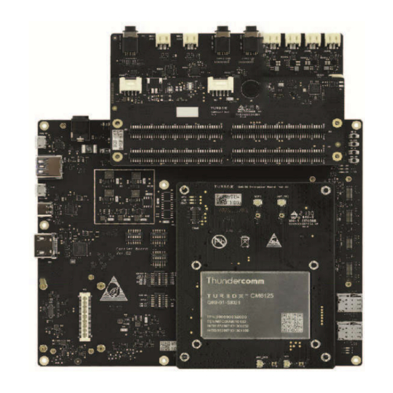
Chapter 1. Product Overview The TurboX CM6125 development kit is a cost-effective solution to evaluate the performance and build the prototype of the smart cameras and intelligent IoT devices quickly. The development kit features rich interfaces, including Type-C USB, LCD, and camera modules. The development kit supports Android-S operating system, combining powerful artificial intelligence and machine learning to address increasing demand for smart cities, commercial and enterprise, homes, and vehicles applications. -
Page 4: Features And Specifications
1.1. Features and specifications Table 1-1. Features and specifications Item Specification CPU: Customized 64-bit Arm v-8.0 compliant applications processor (Qualcomm® Kryo™ 260 CPU) Kryo Gold: quad-core (2.0 GHz high-performance) Kryo Silver: quad-core (1.8 GHz low-power) Processor GPU: Qualcomm® Adreno™ GPU 610 at 950 MHz graphics processing unit (GPU) with 64-bit addressing DSP: Qualcomm®... -
Page 5: Product Diagram
1.2. Product diagram Figure 1-2. Main Board Block Diagram NOTE: Camera module and TFT-LCD are accessories to the development kit. Figure 1-3. Interposer Board Block Diagram - 4 -... -
Page 6: Development Kit Introduction
1.3. Development kit introduction TurboX CM6125 DK adopts TCSOM_Carrier which consists of various sub boards. CM6125 SOM is connected to the DK via the Interposer Board. Main Board Core board of TCSOM_Carrier, adaptable to various SOMs via 500-pin connector. It mainly supports functions of USB, LCM, HDMI out, camera, SD card, SIM card, key, LED, etc. - Page 7 1.1.1. Main Board overview Figure 1-4. Main Board Overview Table 1-2. Main Board interface list Item Reference Description J600 12V DC jack input, 2.5mm/5.5mm USB3400 UART debug port, UART to USB J3901 USB Type-A port, only as host USB3900 Micro USB port, sharing DP/DM with USB Type C connector, adb/download/host/device J3900 USB Type-C port, adb/download/host/device J3800...
- Page 8 Item Reference Description 6-pin switch, boot configuration and CBL SW1, SDM_WDOG_DISABLE SW2, SDM_FAST_BOOT_0 SW3, SDM_FAST_BOOT_1 SW4404 SW4, SDM_FAST_BOOT_2 SW5, SDM_FAST_BOOT_3 SW6, CBL_PWR_N SW4403 Key, Force USB boot button SW4401 Key, Volume up button SW4402 Key, Volume down button SW4400 Key, Power on button...
- Page 9 1.1.2. Interposer Board overview Figure 1-5. Interposer Board Overview Table 1-3. Interposer Board interface list Item Reference Description J1600 ANT_2G_5G_WLAN, Wi-Fi 2.4G/5G&BT J1400 Camera module connector, CSI4 J1602 ANT_DRX, 2G+3G+4G RF Diversity RX J1606 ANT_GPS_L1_IN, GPS, GLONASS, BeiDou, Galileo, QZSS, SBAS J1000 CM6125 SOM J1604...
- Page 10 1.1.3. Audio Board overview Figure 1-6. Audio Board Overview Table 1-4. Audio Board interface list Item Reference Description J900 J901 Low-speed connector to low-speed expansion board J902 4 x 80-pin B2B connector J903 SW3400 SW3401 SW3402 DIP switch for DMIC connection selection SW3403 SW3404 SW3100...
- Page 11 1.1.4. Sensor Board overview Figure 1-7. Sensor Board Overview Table 1-5. Sensor Board interface list Item Reference Description J900 J901 Low-speed connector to low-speed expansion board J902 4 x 80-pin B2B connector J903 J4102 NFC antenna connector J4103 U3103 ALS+ PROXIMITY sensor, TMD2755 U3100...
-
Page 12: Dip Switches
1.4. DIP switches 1.4.1. DIP switches on Main Board SW1300 and SW1301 (for function configuration) Table 1-6. State description of SW1300 Name Function default Control CSI0 switch for CAM0 or Camera Expansion Board 1 CSI0_HDMI_SEL OFF: Use CAM0 on Main Board ... - Page 13 SW2200 (for display function configuration) Name Function Default Connect PM_PWM_A to low speed interface as GPIO 1 PM_PWM_A_LS OFF - / ON –connect this signal to low speed con Connect PM_PWM_A to LCD0 for dimming backlight 2 LCD0_BL_PWM_T ...
- Page 14 Table 1-9. State description of SW2101 Name Function Default Connect CAM1_SPI_CS to low speed interface as GPIO 3 CAM1_SPI_CS_LS OFF- / ON –connect this signal to low speed con Connect CAM1_SPI_CS to CAM1 for SPI communication 4 CAM1_SPI_CS_CON ...
- Page 15 DMIC connection settings: SW3400: ON/ON/OFF/OFF/OFF/OFF, connecting SOM DMIC01 SW3401: OFF/OFF/OFF/OFF/ON/ON, connecting SOM DMIC23 SW3403: OFF/OFF/ON/ON/OFF/OFF, connecting SOM DMIC45 SW3402 & SW3404: OFF/OFF/OFF/OFF/OFF/OFF - 14 -...
-
Page 16: Chapter 2. Specifications For Cm6125 Dk
Chapter 2. Specifications for CM6125 DK 2.1. Main Board 2.1.1. Power-on Step 1. Connect the device (via the UART debug port, No. 2 in Figure 1-4) to a PC with a Micro USB cable. Step 2. Run the serial console tool on host PC (for example: minicom). ... - Page 17 2.1.2. Camera interface Camera interfaces: No.8 to No.13 in Figure 1-4. There are 6 x 4L camera BTB (Board to Board) interfaces on the Main Board. Also, there is a 90-pin connector to expand camera or HDMI in interface on the camera module (see Figure 1-2.
- Page 18 Table 3-1. Camera interface description Name Description STROBE Camera strobe for flash driver (FLASH_STROBE), only for CAM0 SPI_CLK Reserved for Camera SPI communication interface, only for CAM0 AVDD_2V8 SPI_MOSI Reserved for Camera SPI communication interface, only for CAM0 CSI_C1_LN2_P CSI_A2_LN2_M CSI_B0_LN0_P CSI_C0_LN0_M CSI_B2_LN3_P...
- Page 19 2.1.3. Display interface LCD0: No.30 in Figure 1-4 HDMI out interface: No.5 in Figure 1-4 2.1.3.1. LCM The LCM on the Main Board is connected to 5-inch 1280*720 TFT-LCD with touch panel, fixed by a dedicated holder. Check the connection between the LCD panel (accessory) and the board, refer to Figure 2-3. For detailed information on how to open LCM, refer to the relevant software user manual.
- Page 20 Table 3-2. LCM pin definition Symbol Description LED- Backlight cathode LED+ Backlight anode Ground TP-SDA IIC signal of TP TP-SCL TP-INT INT signal of TP TP-RST Reset signal of TP TP-VDD(2.8V) Power supply 2.8V for TP LCD-ID1 AVDD5.5V Power supply of 5.5V AVEE-5.5V Power supply of -5.5V VDD1.8V...
- Page 21 2.1.3.2. HDMI out There is one HDMI out interface on the Main Board. A DSI to HDMI Bridge (LONTIUM SEMICONDUCTOR LT9611UXC) performs this task and supports a resolution from 1080P to 4K at 60Hz. This bridge also supports the audio function performed by a 1-bit I2S on SOMs. For detailed information on how to open HDMI out, refer to the relevant software user manual.
- Page 22 2.1.5. Type-C port The Main Board can implement a USB Type-C port (USB3900), No. 4 in Figure 1-4. Figure 2-5. USB Type-C Port Connection This integrated Type-C port is connected to CM6125 USB0. It supports adb and firmware upgrade, as well as charger, DRD, DP.
- Page 23 Figure 2-7. SD Card Slot 2.1.8. Buttons Four buttons are available on the Main Board. SW4400: power on button, (No. 25 in Figure 1-4), serves as the Power ON/OFF/Sleep button. You can press and hold the button for more than 3 seconds to power on the device. SW4401: volume up button (No.
- Page 24 Figure 2-9. Locate LEDs - 23 -...
- Page 25 2.1.10. Boot config switch A 6-pin DIP (Double In-line Package) switch (No. 21 in Figure 1-4) is located at the top of the Main IO Board. Figure 2-10. Boot Config Switch Pin#1, 2, 3, and 4 are used for boot configuration. ...
- Page 26 2.1.11. Camera expansion connector No. 29 in Figure 1-4 This connector is used to expand the camera board, including camera module and HDMI in. For more information on the camera expansion connector pin-outs, refer to Table 6-1. Table 3-4. Camera expansion connector pin-outs Name Name CAM0_SDA_EXT...
- Page 27 Name Name UART_RTS_EXT CSI1_A2_LN2_M_HS UART_RXD_EXT CSI1_C1_LN2_P_HS UART_TXD_EXT CAM1_XHS_EXT CSI1_A0_CLK_M_HS CAM1_XVS_EXT CSI1_NC_CLK_P_HS CAM1_RST_EXT CAM1_DVDD_1V2_EN_EXT CSI1_B1_LN1_M_HS CAM1_AVDD_2V8_EN_EXT CSI1_A1_LN1_P_HS CAM1_SCL_EXT CSI1_C0_LN0_M_HS CAM1_SDA_EXT CSI1_B0_LN0_P_HS 2.1.12. Display expansion connector This connector is used to expand the display board. For more information on the camera expansion connector pin-outs, refer to Table 3-4. Table 3-5.
- Page 28 Name Name VDC_1V8 VDC_3V3 VDC_1V8 VDC_3V3 VDC_3V3 VDC_1V8 VDC_3V3 VDC_1V8 LCD1_VSN_EN_EXT VDC_5V LCD1_BL_PWM_EXT VDC_5V FLASH_LED1_EXT FLASH_LED2_EXT HDMI_OUT_I2C_SCL_EXT HDMI_OUT_I2C_SDA_EXT DSI1_NC_LN3_M_EXT HDMI_OUT_RSTN_EXT DSI1_C2_LN3_P_EXT HDMI_OUT_INT_EXT LCD1_VSP_EN_EXT DSI1_B2_LN2_M_EXT LCD1_BL_EN_EXT DSI1_A2_LN2_P_EXT LCD1_RESET_N_EXT LCD1_TE_EXT DSI1_C1_CLK_M_EXT TP1_INT_EXT DSI1_B1_CLK_P_EXT TP1_RST_EXT LCD1_VDD_1V8_EN_EXT DSI1_A1_LN1_M_EXT LCD1_VDD_2V8_EN_EXT DSI1_C0_LN1_P_EXT TP1_SCL_EXT DSI1_B0_LN0_M_EXT TP1_SDA_EXT DSI1_A0_LN0_P_EXT - 27 -...
- Page 29 2.1.13. PCIe expansion connector NO. 7 in Figure 1-4 This connector is used to expand the PCIe board. For pin-outs of the high-speed expansion connector, refer to Table 3-5. Table 3-6. High-speed expansion connector pin-outs Name Name PCIE1_REFCLK_M PCIE2_REFCLK_M PCIE1_REFCLK_P PCIE2_REFCLK_P PCIE1_RX0_M PCIE2_RX0_M...
-
Page 30: Interposer Board
2.2. Interposer Board 2.2.1. Wi-Fi/Bluetooth and GPS connection The SOM supports Wi-Fi/BT function via the Wi-Fi antenna connector (No.1 in Figure 1-5). Figure 2-11. Wi-Fi/BT Antenna Connector The SOM supports GPS function via the GPS antenna connector (No.4 in Figure 1-5). - Page 31 2.2.2. 2G/3G/4G connection The SOM supports 2G/3G/4G via the primary antenna connector (No.6 in Figure 1-5) and DRX antenna connector (No. 3 in Figure 1-5). Figure 2-13. Primary Antenna Connector Figure 2-14. DRX Antenna Connector - 30 -...
-
Page 32: Audio Board
2.3. Audio Board This section descripts functions located on the Audio Board. NOTE: Make sure to set the DIP switches should be set to the right state (see 1.4.2. DIP switches on Audio Board). 2.3.1. Speaker connector CM6125 SOM supports dedicated SoundWire interface for smart speaker amplifier, WSA8835. The maximum output power is 7.3W into 8Ω... -
Page 33: Sensor Board
2.3.3. DMIC CM6125 SOM supports three DMIC arrays, connected to SoC. Figure 2-17. DMIC Arrays 2.4. Sensor Board 2.4.1. Sensor CM6125 SOM implements five-sensor IC. Refer to Figure 1-7. 2.4.2. Battery connector No. 8 in Figure 1-7 Table 3-7. Pin definition of battery connector Name Description VBAT_SOM... - Page 34 2.4.3. Fan connector Step 1. Refer to Figure 3-11 to connect a fan to the board via the fan connector (No.10 in Figure 1-5). Figure 2-18. Fan Connector Table 3-1. Fan function Function FAN_VCC, default 12V - 33 -...
-
Page 35: Appendix 1. Compliance And Certificate Information
Appendix 1. Compliance and Certificate Information FCC Statements: OEM/Integrators Installation Manual Important Notice to OEM integrators 1. This module is limited to OEM installation ONLY. 2. This module is limited to installation in mobile or fixed applications, according to Part 2.1091(b). 3. - Page 36 (3) Only antennas of the same type and with equal or less gains as shown below may be used with this module. Other types of antennas and/or higher gain antennas may require additional authorization for operation. Antenna type BT&2.4GHz 5.2GHz band 5.3GHz band 5.5GHz band 5.8GHz band...
- Page 37 Federal Communication Commission Interference Statement This device complies with Part 15 of the FCC Rules. Operation is subject to the following two conditions: (1) This device may not cause harmful interference, and (2) this device must accept any interference received, including interference that may cause undesired operation.
- Page 38 EU Regulatory Conformance Hereby, Thundercomm Technology Co., Ltd declares that this device is in compliance with the essential requirements and other relevant provisions of Directive 2014/53/EU. The device for operation in the band 5150–5350 MHz is only for indoor use to reduce the potential for harmful interference to co-channel mobile satellite systems.
- Page 39 Frequency Bands Conducted Power dBm FDD 28 TDD 34 TDD 38 TDD 40 TDD 41 - 38 -...
-
Page 40: Appendix 2. Contact Information Of Eu Local Agency
Appendix 2. Contact Information of EU Local Agency Company: Thundercomm Europe GmbH Address: 20, Oskar-von-Miller-Ring, 80333 München, c/o WeWork Contact person: Daodong Zhang E-mail: zhangdd0913@thundercomm.com - 39 -... -
Page 41: Appendix 3. Contact Information Of Us Local Agency
Appendix 3. Contact Information of US Local Agency Company: Thundercomm America Corporation Address: 10180 Telesis Court, Suite 120, San Diego, CA 92121 Contact person: Weiqin Bai E-mail: weiqin.bai@thundercomm.com baiwq@thundersoft.com Mobile: +1-8585315328 +86-18618401680 - 40 -... -
Page 42: Appendix 4. Notices
Web sites. The materials at those Web sites are not part of the materials for this Thundercomm product, and use of those Web sites is at your own risk. Thundercomm shall not be responsible for the content of the third party. - Page 43 Internet at your request. Thundercomm has all rights under other relevant exemptions provided by laws and regulations, and Thundercomm's failure to claim or delay in claiming such rights shall not be deemed to be a waiver of such rights by Thundercomm.
-
Page 44: Appendix 5. Trademarks
Appendix 5. Trademarks Thundercomm, Thundercomm TurboX, TURBOX, Thundersoft turbox are trademarks of Thundercomm Corporation or its associate companies in China and/or other countries. Intel, Intel SpeedStep, Optane, and Thunderbolt are trademarks of Intel Corporation or its subsidiaries in the U.S. and/or other countries. - Page 45 Antenna trace interpretation Trace of WIFI 2.4/5G, The width is 0.3175mm and the length is 27.75mm. Impedance: 50ohm, keep out cooper of L2 under the trace.
- Page 46 Trace of Primary antenna, CM6125 only The width is 0.3175mm and the length is 27.75mm. Impedance: 50ohm, keep out cooper of L2 under the trace..
- Page 47 Trace of Diversity antenna, CM6125 only The width is 0.3175mm and the length is 18.5mm. Impedance: 50ohm, keep out cooper of L2 under the trace.
- Page 48 Trace of GPS antenna, CM6125 only The width is 0.3175mm and the length is 17.98mm. Impedance: 50ohm.
Need help?
Do you have a question about the TurboX CM6125 and is the answer not in the manual?
Questions and answers