Table of Contents
Advertisement
Quick Links
Advertisement
Table of Contents

Related Manuals for Avnet Xilinx Zynq 7Z045

Summary of Contents for Avnet Xilinx Zynq 7Z045
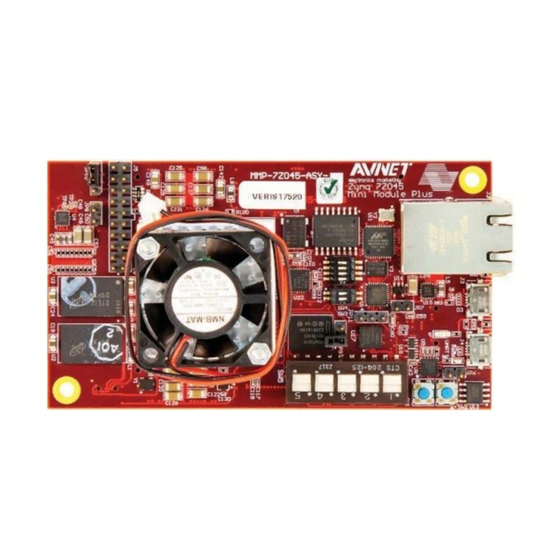
- Page 1 Zynq 7Z045 Mini-Module Plus Development Kit Version 1.0 Page 1 Copyright © 2017 Avnet, Inc. AVNET, “Reach Further,” and the AV logo are registered trademarks of Avnet, Inc. All other brands are the property of their respective owners. LIT# 5151-GSG-AES-7Z7045-G-01-V1...
- Page 2 Document Control Document Version: Document Date: 8/28/2013 Revision History Version Date Comment 8/28/2013 Initial release for production board (AES-MMP-7Z045-G Revision B) Page 2...
- Page 3 Upon completion, be sure to retain your login and password information for future visits to Avnet’s DRC. Logging in once gives you unlimited access to all technical support files and downloads. You will also have the chance to request email notifications whenever there are updates to your design kit.
- Page 4 (collectively “Marks”) are the properties of their respective owners. Avnet disclaims any proprietary interest in Marks other than its own. Avnet and AV design logos are registered trademarks and service marks of Avnet, Inc. Avnet’s Marks may be used only with the prior written permission of Avnet, Inc.
-
Page 5: Table Of Contents
Description .......................... 8 Board Features ........................8 Reference Designs ......................8 Ordering Information ......................9 Functional Description ..................10 Xilinx Zynq 7Z045 AP SoC ....................11 GTX Interface ........................11 2.2.1 GTX Reference Clock Inputs ................12 2.2.2 PCI Express x4 Interface ................. 13 2.2.3... - Page 6 Figures Figure 1 – Zynq 7Z045 Mini-Module Plus Development Board Picture ......9 Figure 2 – Zynq 7Z045 Mini-Module Plus Development Board Block Diagram ..10 Figure 3 – GTX Clock Sources on the Zynq 7Z045 Mini-Module Plus Development Board ..12 Figure 4 –...
- Page 7 Tables Table 1 – Ordering Information ................... 9 Table 2 – Zynq 7Z045 AP SoC Features ..............11 Table 3 – GTX Interface Pin Assignments ..............12 Table 4 – GTX Pin Assignments for PCI Express ............. 14 Table 5 – GTX Pin Assignments for Baseboard FMC, SFP, DP and SMA Connectors ..15 Table 6 –...
-
Page 8: Introduction
The purpose of this manual is to describe the functionality and contents of the Zynq 7Z045 Mini-Module Plus Development Kit from Avnet Electronics Marketing. This document includes instructions for operating the board, descriptions of the hardware features and explains out-of-the-box design code programmed in the on-board QSPI flash. -
Page 9: Ordering Information
The following table lists the development kit part number. Internet link at www.em.avnet.com/MMP-7Z045-G. Part Number Hardware AES-MMP-7Z045-G Xilinx Zynq 7Z045 Mini-Module Plus Development Kit populated with an XC7Z045 FFG900 – 1 speed grade device Table 1 – Ordering Information Page 9... -
Page 10: Functional Description
2 Functional Description A high-level block diagram of the Zynq 7Z045 Mini-Module Plus development board is shown below followed by a brief description of each sub-section. Figure 2 – Zynq 7Z045 Mini-Module Plus Development Board Block Diagram Page 10... -
Page 11: Xilinx Zynq 7Z045 Ap Soc
Xilinx Zynq 7Z045 AP SoC The Zynq 7Z045 AP SoC device available in the FFG900 package has an impressive list of features. The device is made up of two main systems one of which is the Processing System (PS) and the other Programmable Logic (PL). The table below lists some of the 7Z045 features. -
Page 12: Gtx Reference Clock Inputs
GTX Bank GTP Interface Lanes Number 7Z045 GTX0_109 GTX_XDY3 GTX1_109 GTX_XDY2 Display Port GTX2_109 GTX_XDY1 GTX3_109 GTX_X0Y0 PCI Express x4 GTX3_112 GTX_X0Y15 GTX2_112 GTX_X0Y14 GTX1_112 GTX_X0Y13 GTX0_112 GTX_X0Y12 Table 3 – GTX Interface Pin Assignments 2.2.1 GTX Reference Clock Inputs Each GTX bank has reference clock inputs. -
Page 13: Pci Express X4 Interface
2.2.2 PCI Express x4 Interface One of the GTX transceiver banks is connected to the PCI Express x4 card edge interface on the Mini- Module Plus Baseboard 2. PCI Express is an enhancement to the PCI architecture where the parallel bus has been replaced with a scalable, fully serial interface. -
Page 14: Gtx For Fmc Expansion Connector, Sfp, Display Port And Sma (Baseboard)
The PCI Express transmit lanes are AC coupled (DC blocking capacitors are included in the signal path) on the baseboard as required by the PCI Express specification. Bank 112 GTX Instance Net Name 7Z045 Pin # GTX_X0Y15 JX2_MGTTX2_P (PCIE LANE 0) JX2_MGTTX2_N JX2_MGTRX2_P JX2_MGTRX2_N... -
Page 15: Memory
Bank 109 GTX Instance Net Name 7Z045 Pin # JX1_MGTTX3_P JX1_MGTTX3_N GTX_X0Y0 (SMA) JX1_MGTRX3_P JX1_MGTRX3_N JX1_MGTTX2_P JX1_MGTTX2_N GTX_X0Y1 (Display Port) JX1_MGTRX2_P JX1_MGTRX2_N JX1_MGTTX1_P JX1_MGTTX1_N GTX_X0Y2 (SFP) JX1_MGTRX1_P JX1_MGTRX1_N JX1_MGTTX0_P AK10 JX1_MGTTX0_N GTX_X0Y3 (FMC) JX1_MGTRX0_P AH10 JX1_MGTRX0_N Table 5 – GTX Pin Assignments for Baseboard FMC, SFP, DP and SMA Connectors Memory The Zynq 7Z045 Mini-Module Plus Development Board is populated with both high-speed RAM and non-volatile ROM to support various types of applications. -
Page 16: Figure 5 - Ddr3 Sdram Interface
Figure 5 – DDR3 SDRAM Interface The DDR3 signals are connected to bank 502 of the 7Z045. The 7Z045 VCCO pins for the bank 502 are connected to 1.5 V. This supply rail can be measured at the test point labeled 1.5_1.35 V On the Mini-Module Plus Baseboard 2. -
Page 17: Table 6 - 7Z045 Pin Assignments For Ddr3
All DDR3 signals are compliant to the Xilinx recommended and MIG generated pin out. The following table contains the ZYNQ PL pin assignments used for the DDR3 SDRAM interface. Net Name 7Z045 Pin Net Name 7Z045 Pin DDR3_D0 DDR3_A0 DDR3_D1 DDR3_A1 DDR3_D2 DDR3_A2... -
Page 18: Parallel Flash Interface
2.3.2 Parallel Flash Interface The parallel flash memory consists of a single 128 MB Micron device in a 64-ball BGA package, part number PC28F00AP30TFA. The PC28F device is an asynchronous memory that also supports a synchronous-burst read mode for high-performance applications. The PC28F device has a 100 nanosecond access time. -
Page 19: Qspi Flash Interface
The following table contains the ZYNQ PL pin number assignments for the Flash interface. Net Name 7Z045 Pin # Net Name 7Z045 Pin # PFLASH_A1 PFLASH_D0 PFLASH_A2 PFLASH_D1 PFLASH_A3 PFLASH_D2 PFLASH_A4 PFLASH_D3 PFLASH_A5 PFLASH_D4 PFLASH_A6 PFLASH_D5 PFLASH_A7 PFLASH_A8 PFLASH_D6 PFLASH_A9 PFLASH_D7 PFLASH_A10 PFLASH_D8... -
Page 20: I 2 C Eeprom Interface
The figure below shows the interface between the SPI flash and the 7Z045 AP PSoC Figure 7 – 7Z045 QSPI Flash Interface To configure the 7Z045 using the QSPI flash interface the configuration mode for the 7Z045 must be set to QSPI mode. This is accomplished by setting the configuration mode switches to the proper setting. -
Page 21: Clock Sources
Clock Sources The Zynq 7Z045 Mini-Module Plus Development Board used in conjunction with the Mini-Module Plus Baseboard 2 includes all of the necessary clocks to implement high-speed logic and GTX transceiver designs. Most of these master clocks are sourced from the baseboard’s FMC connector and the on-board LVDS clock synthesizer. -
Page 22: Cdcm61001 Programmable Lvds Clock Synthesizer
The on-board 200 MHz LVDS oscillator provides the system clock input to the global clock tree. This 200 MHz clock can be used in conjunction with the 7Z045’s internal clock generators to generate the various logic clocks and the clocks forwarded to the DDR3 SDRAM devices. Additionally, there is an on-board 33 MHz LVTTL clock source connected to bank 500 and serves as the PS system clock. -
Page 23: Table 9 - Cdcm61001 Clock Synthesizer Pin Description
Signal Name Direction Pull Up/Pull Down Description PR[1:0] Input Pull up Prescaler and Feedback divider control pins. OD[2:0] Input Pull up Output divider control pins. OS[1:0] Input Pull up Output type select control pins. Input Pull up Chip enable. RST_N Input Pull up Device reset (active low). -
Page 24: Communication
Communication The Zynq 7Z045 Mini-Module Plus Development Board utilizes Ethernet, USB 2.0 (Host mode or Endpoint) and USB UART physical layer transceivers for communication purposes. Network access is provided by a single 10/100/1000 Mb/s Ethernet PHY device, which is connected to 7Z045 via a standard RGMII interface. -
Page 25: Usb Uart
The following tables provide the 7Z045 pin assignments for the Ethernet PHY interface. Net Name 7Z045 Pin # Net Name 7Z045 Pin # ETH_MDC ETH _RST# B24 or SW1 ETH _MDIO ETH _RX_CTRL ETH _TX_CTRL ETH_RX_CLK ETH_TX_CLK ETH _RX_D0 ETH _TX_D0 ETH _RX_D1 ETH _TX_D1 ETH _RX_D2... -
Page 26: Real-Time Clock (Rtc)
The table below shows the pin assignments of the USB 2.0 PHY to the 7Z045 Net Name 7Z045 Pin # Net Name 7Z045 Pin # USB_D0 USB_D6 USB_D7 USB_D1 USB_STP USB_D2 USB_NXT USB_D3 USB_DIR USB_D4 USB_CLK USB_D5 USB_RESET# A18 or SW2 Table 13 –... -
Page 27: Configuration
Configuration The Zynq 7Z045 Mini-Module Plus Development Board supports several methods of configuring the 7Z045 PSoC. The possible configuration sources include Boundary-scan (JTAG cable), QSPI and Micro SD card. The blue LED D1 labeled “DONE” on the baseboard illuminates to indicate when the 7Z045 has been successfully configured. -
Page 28: Pjtag Interface (Arm Dap)
Figure 11 – JTAG Interface Programming the 7Z045 via Boundary-scan mode requires a JTAG download cable. For more information about JTAG download cables, perform a search on the Xilinx web page using the key words “Programming Cables”. www.xilinx.com JP10 can be used to allow the JTAG programmer’s reset pin to assert the 7Z045 PS_SRST# signal. If using the Xilinx PC4 JTAG module (14-pin connector) the reset output on the cable is pin 14. -
Page 29: Expansion Connectors
Expansion Connectors The Zynq 7Z045 Mini-Module Plus Development Board connects to the Mini-Module Plus Baseboard 2 via two 120 pin connectors referenced on the board as JX1 and JX2. These two connectors provide all of the power required to operate the module as well as provide I/O to the baseboard’s peripheral interfaces. -
Page 30: Table 17 - Jx1 Pin Assignments And Baseboard Signal Mapping
BB2 Connector I/O Connector 7Z045 7Z045 I/O Connector BB2 Connector Signal Name Signal Name Pin # Pin # Pin # Pin # Signal Name Signal Name JX1_MGTRX2_N JX1_MGTTX2_N DP_ML_L0_N SMA_RX_P JX1_MGTRX3_P JX1_MGTTX3_P SMA_TX_P SMA_RX_N JX1_MGTRX3_N JX1_MGTTX3_N SMA_TX_N CLK_MUX_OUT_ JX1_MGTREFCLK_P AD10 MGTAVTT (1.2V) CLK_MUX_OUT_ JX1_MGTREFCLK_N... - Page 31 BB2 Connector I/O Connector 7Z045 7Z045 I/O Connector BB2 Connector Signal Name Signal Name Pin # Pin # Pin # Pin # Signal Name Signal Name JTAG_TCK MMP_JTAG_TCK MMP_JTAG_TMS JTAG_TMS JX2_SE_IO_0_P AA30 JX2_SE_IO_0_N JX2_SE_IO_2_P AA29 JX2_SE_IO_2_N SFP0_TX_FAULT_VT JX2_SE_IO_4_P AG26 AG27 JX2_SE_IO_4_N SFP0_TX_DISABLE SFP0_MOD2_VT...
-
Page 32: Table 18 - Jx2 Pin Assignments And Baseboard Signal Mapping
BB2 Connector I/O Connector 7Z045 7Z045 I/O Connector BB2 Connector Signal Name Signal Name Pin # Pin # Pin # Pin # Signal Name Signal Name VCCAUX VCCAUX FMC1-LA18-CC_P JX2_DIFF_IO_2_P JX2_DIFF_IO_3_P FMC1-LA20_P FMC1-LA18-CC_N JX2_DIFF_IO_2_N JX2_DIFF_IO_3_N FMC1-LA20_N VCCAUX 2.5 V FMC1-LA23_P JX2_DIFF_IO_4_P JX2_DIFF_IO_5_P FMC1-LA19_P... -
Page 33: 2.10 Power
2.10 Power The Zynq 7Z045 Mini-Module Plus Development Board’s power is sourced from the Mini-Module Plus baseboard 2 via the JX1 and JX2 connectors. Below is a diagram that illustrates the voltage rails sourced by the baseboard. Figure 12 - Power Supply Diagram FMC_VADJ, VCC_AUX and the 1.5 V voltage rails are selectable from the baseboard. -
Page 34: 2.11 Thermal Management
Refer the Mini-Module plus Baseboard 2 User’s Guide on the DRC for more detailed information about the baseboard power system. www.em.avnet.com/en-us/design/drc/Pages/Mini-Module-Plus-Baseboard-2.aspx 2.11 Thermal Management An active heat sink is used to dissipate heat from the 7Z045. A Cool Innovations heat sink (PN: 3-121204UBFA) and an NMB 12 V fan (PN: 1204KL-04W-B50-B00) are assembled together and shipped with the Zynq 7Z045 Mini-Module Plus. -
Page 35: Pre-Programmed Memory
NOTE: The PC or laptop will require the Silicon Labs CP210x driver be installed in order to use the USB UART interface. These drivers can be found at the Silicon Labs website or on the Avnet Zynq 7Z045 Mini-Module Plus DRC site under the “Support and Downloads” link. -
Page 36: Appendix A - Assembly Drawing And Jumper Definitions
Appendix A – Assembly drawing and Jumper Definitions This section provides a description of the jumper settings for the Zynq 7Z045 Mini-Module Plus Development Board. The board is ready to use out of the box with the default jumper settings. The following assembly drawing of the component side of the board shows the location of the jumpers followed by a brief description of the jumper functions.
Need help?
Do you have a question about the Xilinx Zynq 7Z045 and is the answer not in the manual?
Questions and answers