Table of Contents
Advertisement
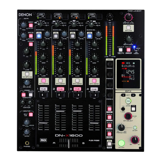
MODEL
DN-X1600
• For purposes of improvement, specifications and design are subject to change without notice.
• Please use this service manual with referring to the operating instructions without fail.
• Some illustrations using in this service manual are slightly different from the actual set.
S0144-1V03DM/DG1009
SERVICE MANUAL
JP
DJ MIXER
D&M Holdings Inc.
Copyright 2010 D&M Holdings Inc. All rights reserved.
WARNING: Violators will be prosecuted to the maximum extent possible.
E3
E2
EK
K2A E1C E1K EUT
P P
Ver. 3
Please refer to the
MODIFICATION NOTICE.
Advertisement
Table of Contents

Related Manuals for Denon DN-X1600


Summary of Contents for Denon DN-X1600
- Page 1 MODIFICATION NOTICE. SERVICE MANUAL MODEL K2A E1C E1K EUT DN-X1600 DJ MIXER • For purposes of improvement, specifications and design are subject to change without notice. • Please use this service manual with referring to the operating instructions without fail. • Some illustrations using in this service manual are slightly different from the actual set.
-
Page 2: Safety Precautions
SAFETY PRECAUTIONS The following check should be performed for the continued protection of the customer and service technician. LEAKAGE CURRENT CHECK Before returning the unit to the customer, make sure you make either (1) a leakage current check or (2) a line to chassis resistance check. -
Page 3: Note For Schematic Diagram
NOTE FOR SCHEMATIC DIAGRAM WARNING: Parts marked with this symbol z have critical characteristics. Use ONLY replacement parts recommended by the manufacture CAUTION: Before returning the unit to the customer, make sure you make either (1) a leakage current check or (2) a line to chassis resistance check. If the leakage current exceeds 0.5 milliamps, or if the resistance from chassis to either side of the power cord is less than 460 kohms, the unit is defective. -
Page 4: Technical Specifications
TECHNICAL SPECIFICATIONS n GENERAL n AUDIO (0 dBu = 0.775 Vrms, 0 dBV = 1 Vrms) • PHONO inputs Stereo x 3 Unbalanced RCA terminal USB MIDI I/O: IN: 1ch, OUT: 1ch MIDI1.0, Input impedance: 47 kΩ/kohms MIDI Clock USB B Level: –40 dBV (10 mV) MIDI OUT: OUT: 1ch MIDI1.0, • CD inputs Stereo x 5 Unbalanced RCA terminal MIDI Clock 5pin DIN Input impedance: 10 kΩ/kohms Channel level meters: PPM 16-point LEDs from –40 to +10 dB, Level: 0 dBV peak display • Equalizer (LINE) Band x 3 Cue master level meters: Channel equalization adjustment range: ... - Page 5 DISASSEMBLY • Disassemble in order of the arrow of the figure of following flow. • In the case of the re-assembling, assemble it in order of the reverse of the following flow. • In the case of the re-assembling, observe "attention of assembling" it. •...
- Page 6 About the photos used for descriptions in the DISASSEMBLY" section. • The direction from which the photographs used herein were photographed is indicated at "Direction of photograph: ***" at the left of the respective photographs. • Refer to the table below for a description of the direction in which the photos were taken. •...
- Page 7 1. TOP CHASSIS SUB ASSY Proceeding : TOP CHASSIS SUB ASSY (1) Remove the screws and the knobs. KNOB KNOB (2) Remove the screws. Direction of photograph: A Direction of photograph: B Direction of photograph: C Direction of photograph: D...
- Page 8 (3) Disconnect the connector wire and FFC Cable, and remove the sheet. Open the wire clamper. SHEET WIRE CLAMPER FFC Cable Direction of photograph: B CX071...
- Page 9 2. TOP PANEL UNIT Proceeding : TOP CHASSIS SUB ASSY TOP PANEL UNIT → (1) Remove the knobs. (2) Remove the screws. (3) Remove the Nuts and Lens rings. LENS RING LENS RING...
- Page 10 (4) Disconnect the FFC Cable. Remove the secrews. FFC Cable...
-
Page 11: Input Unit
3. INPUT UNIT Proceeding : TOP CHASSIS SUB ASSY INPUT UNIT → (1) Remove the screws. Remove the Nuts and Washers. Direction of photograph: A WASHER (2) Remove the screws.Disconnect the FFC Cables. FFC Cable FFC Cable... - Page 12 4. OUTPUT UNIT, MAIN UNIT Proceeding : TOP CHASSIS SUB ASSY INPUT UNIT OUTPUT UNIT, MAIN UNIT → → (1) Remove the screws. Remove the Nuts and Washers. Direction of photograph: A WASHER (2) Remove the screws. Disconnect the FFC Cables and the connectors. CY102 STAY PWB STAY PWB...
-
Page 13: Fader Unit
5. FADER UNIT Proceeding : TOP CHASSIS SUB ASSY FADER UNIT → (1) Remove the screws. (2) Remove the screws. Disconnect the connector wires. CONNECTOR CONNECTOR... - Page 14 6. HP UNIT Proceeding : TOP CHASSIS SUB ASSY HP UNIT → (1) Disconnect the connector wire. Remove the Nuts. CY102 (2) Remove the screws. Direction of photograph: D...
- Page 15 7. MIC UNIT Proceeding : TOP CHASSIS SUB ASSY MIC UNIT → (1) Remove the screw. Disconnect the FFC Cable. FFC Cable (2) Remove the screws. Remove the Nut and Washer. Direction of photograph: D WASHER (3) Remove the screws. Direction of photograph: D...
-
Page 16: Power Unit
8. AC INPUT UNIT Proceeding : TOP CHASSIS SUB ASSY AC INPUT UNIT → (1) Disconnect the connector wires and LINK. CX021 CX022 AC INPUT UNIT Direction of photograph: D LINK (2) Remove the screws. Direction of photograph: C 9. POWER UNIT Proceeding : TOP CHASSIS SUB ASSY POWER UNIT →... -
Page 17: Service Mode
SERVICE MODE 1. Launching the service mode and selecting the check mode ・ P ressing the MIC1 ON/OFF and MIC EFX INS button simultaneously, turn on the power. Keep pressing the MIC1 ON/ OFF and MIC EFX INS button until [DENON] is displayed. When the service mode is set, the service mode's top menu appears. ※ The communications mode is set when the power is turned off then turned back on. ・ Contents of the display on the service mode's top menu 1) Func 2) SW Chk 3) VR Chk 4) LED Chk ・ T urn the EFX SELECT control to select each check mode, then press the EFX SELECT control to set each check mode. 2. Mode 2.1. Func (Function Mode) With "Func" is displayed, press the EFX SELECT control. - Page 18 2.3. VR Chk (Panel volume Check)) With "VR Chk" is displayed, press the EFX SELECT control ・ Check the operations of the VR. Turn the VR, VR name and value of "0" ~ "1023" are displayed on the VFD. ・ Check the operations of the rotary encoder. When the rotary encoder is turned, the rotary encoder name and " < " (counterclockwise) or " > " (clockwise) are displayed on the VFD. When the rotary encoder with a switch is pressed, the rotary encoder name and “ ■ ” are displayed on the VDF. ・ Check the operations of the fader VR. Move the fader VR, fader VR name and value of "0" ~ "1023" are displayed on the VFD. ・...
-
Page 19: Version Upgrade Procedure Of Firmware
VERSION UPGRADE PROCEDURE OF FIRMWARE Use the procedure described below to update the firmware to a newer version. ・ Store the file for updating the firmware (file name: X1600FW.BIN) in the root directory of USB device. ・ If the file for updating the firmware is stored on a USB device, connect the USB device to the USB A terminal. Note : D o not turn off the power or disconnect the USB cable or the USB device while the firmware is being updated. If firmware updating is not completed normally, some operations may no longer be guaranteed to work and it may not be possible to update the firmware again. 1) Turn on the power while pressing the MIC2 ON/OFF and DUCKING button simultaneously. (Version up mode) 2) Press the UTILITY button according to the screen display. 3) "* * * * -> * * * *" is scroll displayed. 4) Press the MIDI CLK button to begin updating. (Approximately 40 second are required for updating to be completed.) 5) "Finish!" and "Ver * * * *" are displayed when firmware updating is completed. 6) Turn the power off and disconnect the USB device from the USB port. ABOUT REPLACE THE MICROPROCESSOR WITH A NEW ONE When replaced of the U-PRO (Microprocessor) or the Flash ROM, confirm contents of the following. After PWB Name Ref. No. Description Remark replaced MAIN IC103 EN29LV160BB-70TIP... -
Page 20: Troubleshooting
TROUBLE SHOOTING FLOW CHART NO.1 (8U-110068-1, -2:POWER UNIT) The power cannot be turned on. O.K. N.G. Is the fuse normal? See FLOW CHART NO.2 <The fuse blows out.> O.K. Is normal state restored when once unplugged N.G. power cord is plugged again after several seconds? Check if there is any leak or short-circuiting on the primary circuit component, and replace it if O.K. - Page 21 FLOW CHART NO.3 (8U-110068-1, -2:POWER UNIT) +1.2V is not outputted. O.K. Check if there is any leak or short-circuiting on the N.G. primary circuit component, and replace it if Is the +5V line voltage normal? defective. (C901,C902,C903,C906,C907,C908,L901,L902,T901) O.K. Check IC903 and the periphery circuit, and replace it if defective FLOW CHART NO.4 (8U-110068-1, -2:POWER UNIT) +3.3V is not outputted.
- Page 22 FLOW CHART NO.6 (8U-110068:POWER UNIT) -15VA is not outputted. O.K. N.G. Is the fuse normal? See FLOW CHART NO.2 <The fuse blows out.> O.K. N.G. Is the voltage of -15V or less supplied to IN terminal Check D925 and replace it if defective. of IC906? O.K.
- Page 23 FLOW CHART NO.8 (8U-110069-1:PANEL UNIT) The key operation is not functioning. O.K. Are the contact point and the installation state of the key switches (S401,S402,S404 ~ S426,S441), N.G. Re-install the switches correctly or replace the poor rotary switches (S433 ~ S436), slide switches switch.
- Page 24 FLOW CHART NO.9 (8U-110070-1:EFECT UNIT) The key operation is not functioning. O.K. N.G. Are the contact point and the installation state of Re-install the switches correctly or replace the poor the key switches (S601 ~ S611, S613) normal? switch. O.K. N.G.
- Page 25 FLOW CHART NO.10 (8U-210093:OUTPUT UNIT) Function of sound for master output do not operate normally. O.K. ・Set the line input selector button to "CD". ・Set the fader assign switch to "THRU". ・Set the channel fader to "MAX". Check the input signal from CY232 to IC101 and ・Set the master level control to "MAX".
- Page 26 FLOW CHART NO.11 (8U-210092:INPUT UNIT) Function of sound for master output do not operate normally. O.K. ・Set the line input selector button to "CD". ・Set the fader assign switch to "THRU". ・Set the channel fader to "MAX". Check the input signal from JK101 to IC108 and N.G.
- Page 27 BLOCK DIAGRAM DNX1600 BLOCK DIAGRAM EFFECT RETURN 8U-210092 MIDI OUT USB B FADER ST 8U-310012 DIGITAL OUT MIC1 MIC2 L(MONO) PHONO PHONO PHONO INPUT UNIT MAIN UINT USB A +15V -15V DATA 48MHz LINE1 LINE2 LINE3 LINE4 CPU(USB) +5VA GND(PHONO) LRCK/BCK S.AGND RL_5V...
-
Page 28: Level Diagram
LEVEL DIAGRAM... -
Page 29: Wiring Diagram
WIRING DIAGRAM DNX1600 WIRING DIAGRAM CX181 CY181 CY131 CX131 CX232 CY232 CW102 CY102 S.DGND 1 S.DGND 1 GND 1 GND HP_L 1 HP_L A_RST 2 A_RST CUE1 2 CUE1 A_RST 2 A_RST AG_L 2 AG_L AD_ORS0 3 AD_ORSD PLAY1 3 PLAY1 DA_SCK 3 DA_SCK AG_R... -
Page 30: Printed Wiring Boards
PRINTED WIRING BOARDS 8U-110068-2 (COMPONENT SIDE) 8U-110068-1 (COMPONENT SIDE) 鉛フリー半田 半田付けには、鉛フリー半田 (Sn-Ag-Cu) を使用してください。 Lead-free Solder When soldering, use the Lead-free Solder (Sn-Ag-Cu). - Page 31 8U-110068-2 (FOIL SIDE) 8U-110068-1 (FOIL SIDE) 鉛フリー半田 半田付けには、鉛フリー半田 (Sn-Ag-Cu) を使用してください。 Lead-free Solder When soldering, use the Lead-free Solder (Sn-Ag-Cu).
- Page 32 8U-110069-1 (COMPONENT SIDE) 8U-110069-2 (COMPONENT SIDE) 鉛フリー半田 半田付けには、鉛フリー半田 (Sn-Ag-Cu) を使用してください。 Lead-free Solder When soldering, use the Lead-free Solder (Sn-Ag-Cu).
- Page 33 8U-110069-1 (FOIL SIDE) 8U-110069-2 (FOIL SIDE) 鉛フリー半田 半田付けには、鉛フリー半田 (Sn-Ag-Cu) を使用してください。 Lead-free Solder When soldering, use the Lead-free Solder (Sn-Ag-Cu).
- Page 34 8U-110070-1 (FOIL SIDE) 8U-110070-1 (COMPONENT SIDE) 8U-110070-3 (COMPONENT SIDE) 8U-110070-2 (FOIL SIDE) 8U-110070-2 (COMPONENT SIDE) 8U-110070-3 (FOIL SIDE) 鉛フリー半田 半田付けには、鉛フリー半田 (Sn-Ag-Cu) を使用してください。 Lead-free Solder When soldering, use the Lead-free Solder (Sn-Ag-Cu).
- Page 35 8U-110070-6 (COMPONENT SIDE) 8U-110070-6 (FOIL SIDE) 8U-110070-4 (COMPONENT SIDE) 8U-110070-4 (FOIL SIDE) 8U-110070-5 (COMPONENT SIDE) 8U-110070-5 (FOIL SIDE) 鉛フリー半田 半田付けには、鉛フリー半田 (Sn-Ag-Cu) を使用してください。 Lead-free Solder When soldering, use the Lead-free Solder (Sn-Ag-Cu).
- Page 36 8U-210092 (COMPONENT SIDE) 鉛フリー半田 半田付けには、鉛フリー半田 (Sn-Ag-Cu) を使用してください。 Lead-free Solder When soldering, use the Lead-free Solder (Sn-Ag-Cu).
- Page 37 8U-210092 (FOIL SIDE) 鉛フリー半田 半田付けには、鉛フリー半田 (Sn-Ag-Cu) を使用してください。 Lead-free Solder When soldering, use the Lead-free Solder (Sn-Ag-Cu).
- Page 38 8U-210093 (COMPONENT SIDE) 8U-210093 (COMPONENT SIDE) 鉛フリー半田 半田付けには、鉛フリー半田 (Sn-Ag-Cu) を使用してください。 Lead-free Solder When soldering, use the Lead-free Solder (Sn-Ag-Cu).
- Page 39 8U-110093 (FOIL SIDE) 8U-110093 (FOIL SIDE) 鉛フリー半田 半田付けには、鉛フリー半田 (Sn-Ag-Cu) を使用してください。 Lead-free Solder When soldering, use the Lead-free Solder (Sn-Ag-Cu).
- Page 40 8U-310012 (COMPONENT SIDE) 8U-310012 (FOIL SIDE) 鉛フリー半田 半田付けには、鉛フリー半田 (Sn-Ag-Cu) を使用してください。 Lead-free Solder When soldering, use the Lead-free Solder (Sn-Ag-Cu).
-
Page 41: Schematic Diagrams
+18V AC INLET W908 2350156903 GND-TERMINAL D924 L907 FMX-G26S 22uH L905 22uH P-GND D925 T901 NC FMX-G26S E3/JP L906 JAPAN ONLY A-GND 2061087073 2061087073 2061035041 L908 22uH F901 R902 OPEN 2.2M D915 ET1.6A ET1.6A 2.0(T) 22uH TH901 1SS355 2350156903 NTPAD8R0LDNB0 T901 -18V R955... -
Page 42: Panel Unit
+34V +1.2V +3.3V CX071 L101 7P-DA 22uH AGND +3.3V C114 AGND 1000P R119 R121 R135 R117 R123 R125 R127 R129 R131 R133 R137 R139 R141 R143 R145 R147 +34V FL_GND R181 R187 R188 R192 R178 R179 R180 R182 R183 R184 R185 R186 R189... - Page 43 S433 S434 S435 S436 to FADER(CH4) to FADER(CH3) to XFADER to FADER(CH2) to FADER(CH1) ROTARY-SW ROTARY-SW ROTARY-SW ROTARY-SW LD401 ON(MIC1) ON(MIC2) SEL(LN1) SEL(LN3) SEL(LN4) CY082 CX044 8 10 8 10 SEL(LN2) 8 10 SLR342DC CW046 8P-KRs +3.3V 4P-EHs CW043 4P-SAN CW042 CW045 S401...
-
Page 44: Effect Unit
LD613 LD615 SLR-322MC SLR-322MC LD11 LD601 LD605 LD610 SLR342VC SLI-343D8CT32 SLR342VC LD12 LD602 LD606 LD611 C601 CY233 SLI-343D8CT32 SLR-322MC SLR-322MC 0.1Z 23P-FFCs C602 ADJVOL OPEN LD13 DRY/WETV LD603 LD607 LD612 DGND SLI-343D8CT32 SLR342VC SLR342VC +3.3V SL13 SL13 SL14 LD14 SL14 R664 SL15 SL15... - Page 45 +15V R160 100K R115 R170 100K 3.3K RL_5V C115 100P CY231 C105 R134 100K 23P-FFCs C109 R132 100K RL101 RELAY1 C111 NA5W-K OPEN RELAY2 R101 +5VA RELAY3 (1/2) 3.3K R119 C117 RELAY4 R182 47/50 IC108 A_RST A_RST. A_RST NJM2068MD R154 C130 ADMCLK AD_OSR0...
- Page 46 +15V R315 RL_5V 3.3K C307 RELAY3 C311 C313 RL301 C317 OPEN. NA5W-K 47/50 R301 +5VA (1/2) 3.3K R319 R333 IC301 NJM2068MD A_RST. R317 C321 ADMCLK. OPEN 47/50 ADLRCK. IC303 IC301 ADBCK. SA5532ADR NJM2068MD ADAT3 R321 S.AGND R331 R303 TR301 (2/2) (2/2) 3.3K DTC123J...
- Page 47 TO MAIN UNIT +5VA +5VA +15V R621 CY131 13P-FFC +3.3VD C625 47/50 EFXRTN IC607 C618 SA5532ADR 0.1Z C622 JK606 C795 0.01 PHONE-JACK R619 (2/2) C697 3.3K R607 R625 D602 C635 (1/2) 0.1Z 643010071000S 3.3K C661 OPEN +3.3VA 0.01 C629 C698 R602 R615 0.01...
-
Page 48: Master Out
+15V W102 ST101 W101 S.DGND S.AGND STYLE-PIN GND-TERMINAL GND-TERMINAL 35mm CX101 C136 10P-EH 1000P C144 1000P 2050502006 C137 0.01 C145 0.01 +5VA +3.3V +15V +3.3VA AGND AGND -15V -15V S.DGND S.DGND RE_5V TR110 RE_GND 2SD1898 C105 +5VA C103 470/25 AGND R121 +3V3 DGND... -
Page 49: Booth Out
+15V R643 C643 R623 R637 C653 6.8K 4.7K (1/2) C655 CW102 47/50 10P-SAN IC608 SA5532ADR HP_L AG_L AG_R HP_R +15V -15V R621 R635 RL_MUTE 6.8K 4.7K R622 R638 6.8K 4.7K +5VA +3.3V +3.3VA TR_MUTE S.AGND IC615 PCM1690 RSV2 RSV2 VCC2 RSV1 RSV2 AGND2... - Page 50 +15V G=0dB R682 OPEN R321 6.8K C317 150P S.AGND S.AGND C301 (REC OUT) 220/50 R305 R313 6.8K 3.3K C329 C302 R337 REC_LN 47/25 REC_Lch (1/2) R341 4.7K IC303 NJM2068MD TR301 KTC2875B R307 R317 6.8K 3.3K REC_LP R318 R306 6.8K 3.3K REC_RP R342 IC303...
-
Page 51: Mic Input
+15V. D401 KDS226 R435 C423 MIC INPUT C443 47/16 D403 C435 C425 VR401 KDS226 47/16 5KC(L=20) (1/2) +5VA. CX181 C417 671010027206S PHONE-JACK IC401 18P-FFC JK401 C405 NJM2068MD 644810102503S R405 C421 47/16 R447 S.DGND 3.3K MIC2 TR405 A_RST TR401 2SC3324 2SC3324 C445 AD_ORS0 R441... - Page 52 CX141 OPEN +3V3 +1V2 FB109 V3SH V1SH V3SHA 18PG121 FB110 18PG121 C157 47/16 R104 GRM32 SHDQ16 R167 SHDB16 IC107 R207 SHDQ17 R168 3.3K W9864G2GH-6 SHDB17 PLAY4 SHDQ18 R169 SHDB18 SHDQ19 R170 SHDB19 SHDQ15 SHDQ0 DQ15 SHDQ20 R171 SHDB20 VSSQ R196 VCCQ SHDQ21 R172...
- Page 53 +3V3 CX142 14P-SH V3AS +3V3 FB504 18PG121 1pin 9pin 14pin 27pin 43pin 49pin 1pin 9pin 14pin 27pin 43pin 49pin DSP_CLK DGND IC501 [TOP VIEW] DSP16.9M DSP16.9M R501 OPEN D710E001ZDH300 DSP_CLK V3AS V3AS DSP_CLK DGND R585 OPEN SHDB0 SHDB0 R530 AXRO[6] SHDB1 SHDB0 R527...
- Page 54 +3V3 USB1DAT R415 USB1DAT USB1DAT USBD_1 C16 USB2DAT DGND USB2DAT R416 USB2DAT USBD_2 C15 USB3DAT USB3DAT R417 USB3DAT USBD_3 D15 USB4DAT USB4DAT R418 USB4DAT USBD_4 D16 ADDAT1 ADDAT1 ADDAT1 F11 ADDAT1 ADDAT2 ADDAT2 ADDAT2 ADDAT2 F12 ADDAT3 ADDAT3 ADDAT3 ADDAT3 G11 ADDAT4 /UHPI_HRDY.
- Page 55 CX231 23P-FFC C701 RELAY1 RELAY1 C702 RELAY2 RELAY2 +3V3 C703 RELAY3 RELAY3 C704 RELAY4 RELAY4 R758 C705 A_RST A_RST OPEN C706 AD_OSR0 AD_OSR0 R755 ADLRCK ADLRCK IC703 ADBCK ADBCK AK4125VF FILT AVDD ADDAT1 ADDAT1 C782 AVSS DVSS ADDAT2 ADDAT2 DVDD ADDAT3 ADDAT3 R759...
-
Page 56: Exploded View
EXPLODED VIEW S13X2 S04X3 060X2 TOP CHASSIS SUB ASSY 059X2 S04X2 060X4 062X2 059X12 061X2 S03X3 060X2 059X2 064X4 066X4 059X2 S03X3 S07X2 S03X2 S03X2 014X2 S03X8 S04X4 S04X4 S09X2 S12X2 S11X2 068X6 S10X4 S06X4 S10X4 S12X4 S06X3 S11X4 E3 only E2E3 only S09X4 S06X3... - Page 57 S08X4 S07X2 045X4 049X9 045X3 044X4 S07X3 S07X3 048X2 048X4 S07X3 045X3 045X4 031X11 046X4 S04X2 049X2 047X4 S02X2 032X11 045X2 S13X4 S13X4 S13X12 S13X4 S13X2 S01X8 S03X3 S03X2 045X5 S03X6 S13X2 S03X4 S03X2 S02X2 S02X3 S02X2 S02X2 S02X3 S03X3 S02X6 S02X2 WARNING:...
-
Page 58: Parts List Of Exploded View
PARTS LIST OF EXPLODED VIEW Ref. No. Part No. Part Name Remarks Q'ty BUFFER * Parts for which "nsp" is indicated on this table cannot be supplied. BUFFER * P.W.B. ASS'Y for which "nsp" is indicated on this table cannot be supplied. When repairing the P.W.B. ASS'Y, check the board parts table and order BRACKET CH replacement parts. -
Page 59: Parts List Of Packing View
PACKING VIEW rtyui E3 model Q0 Q 2 PARTS LIST OF PACKING VIEW * Parts for which "nsp" is indicated on this table cannot be supplied. * The parts listed below are for maintenance only, might differ from the parts used in the unit in appearances or dimensions. Note: The symbols in the column "Remarks"... - Page 60 SEMICONDUCTORS Only major semiconductors are shown, general semiconductors etc. are omitted to list. Section 1 Overview The semiconductor which described a detailed drawing in a schematic diagram are omitted to list. 1. IC's Pin Arrangement R5S72630P200FP (IC104) PB2/SCL1/PINT2/IRQ2 AVss PB3/SDA1/PINT3/IRQ3 PA7/AN7/DA1 PVcc PA6/AN6/DA0 PVcc PA5/AN5...
- Page 61 Section 1 Overview Block Diagram R5S72630P200FP Block Diagram SH-2A Floating-point CPU core unit (FPU) CPU instruction fetch bus (F bus) CPU bus (C bus) CPU memory access bus (M bus) (I clock) Instruction Operand On-chip RAM User break Cache cache memory cache memory (high-speed) controller UBCTRG output...
- Page 62 Pin No Pin name Function PC1/A1 FLASH(IC103), FPGA / Address Bus PVCC PVCC SDRAM(IC107),FLASH(IC103) / Address Bus SDRAM(IC107),FLASH(IC103) / Address Bus SDRAM(IC107),FLASH(IC103) / Address Bus SDRAM(IC107),FLASH(IC103) / Address Bus SDRAM(IC107),FLASH(IC103) / Address Bus SDRAM(IC107),FLASH(IC103) / Address Bus SDRAM(IC107),FLASH(IC103) / Address Bus PVCC SDRAM(IC107),FLASH(IC103) / Address Bus PVSS DGND...
- Page 63 Pin No Pin name Function PE12/RXD3 FADER PLAY 3 Output /WAIT ADSP HRDY DGND PVSS DGND RTC_X1 DGND RTC_X2 PVCC PVCC PE13/TXD3 LCD Serial Control DATA @X1700 / NC @X1600 FPGA Configration PE15 FPGA Configration PVSS DGND CPU-DSP FLAG(backup) USB Control PB10 USB Control PB11 USB Control...
- Page 64 Pin No Pin name Function SSISCK3 FPGA / USB Audio Bit clock AUDIO_CLK FPGA / Audio Clock DGND PVSS DGND AUDIO_X1 DGND AUDIO_X2 PVCC PVCC SSIDATA2 FPGA / USB Audio data SSIWS2 FPGA / USB Audio LR clock SSISCK2 FPGA / USB Audio Bit clock PF18/LCD_CL2 LCD CLK @X1700 / NC @X1600 PF19/LCD_CL2...
- Page 65 Pin No Pin name Function PB0/IRQ0 FPGA / Interrupt signal PB1/IRQ1 ADSP / Interrupt signal PB2/IRQ2 ADSP / IIC control Clock PB3/IRQ3 ADSP / IIC control data PVCC PVCC PVCC PVCC PB4/SCL2 (Pull Up) PB5/SDA2 (Pull Up) PVSS DGND DGND PB6/SCL3 (Pull Up) PB7/SDA3 (Pull Up) PD15/D31...
- Page 66 Pin No Pin name Function FLASH(103),ADSP / Data Bus FLASH(103),ADSP / Data Bus FLASH(103),ADSP / Data Bus FLASH(103),ADSP / Data Bus PVSS DGND PVCC PVCC RD/WR SDRAM(IC107) /Write Enable, ADSP UHPI / Select Signals SDRAM(IC107) / Clock Enable /CASU/BREQ FADER PLAY4 OUTPUT...
- Page 67 D710E001ZDH300 (IC501) D710E001ZDH300 Block diagram D710E001ZDH300 Pin Function D710E001ZDH300 Pin Function...
- Page 68 D710E001ZDH300 Pin Function D710E001ZDH300 Terminal Function Pin No BGA Location Pin name Function DGND DGND DVDH DVDH 710LRCK ALL Device LRCK 710BCK ALL Device BCK ACLKR0 Not use EFXSDAT Effect Send Data Output DGND DGND BOOTDAT Booth Out Data Output EFXRDAT Effect Return Data Input DGND DGND USB3DAT USB3 Data Input USB1DAT...
- Page 69 Pin No BGA Location Pin name Function USB4DAT USB4 Data Input USB2DAT USB2 Data Input CH4DAT CH4 Data Input CH2DAT CH2 Data Input SPIO_SOMI IIC control data DSP-CPU DSPGPIO2 GPIO DSP-FPGA DVDH DVDH AMUTE0 Not use DSP_CLK McASP0 Transmit Master Clock SHDB23 UHPI Data Bus [Upper 16 Bits (IO)] HUPI_HBE2 UHPI Byte Enable for UHPI_HD[23:16] DSPHBE...
- Page 70 Pin No BGA Location Pin name Function AFMCE Asynchronous Memory Chip Select EM_RW Asynchronous Read/Write CPU_DSP1 GPIO port DSP-CPU AFSX1 Not use SHDB19 UHPI Data Bus [Upper 16 Bits (IO)] SHDB20 UHPI Data Bus [Upper 16 Bits (IO)] DGND DGND DGND DGND DGND DGND DGND DGND...
- Page 71 Pin No BGA Location Pin name Function OSCVDD CVDL CVDL CVDL DGND DGND DGND DGND DGND DGND DGND DGND DGND DGND DGND DGND CVDL CVDL SHDB15 UHPI Data Bus [Lower 16 Bits] DVDH DVDH AEMA1 EMIF Address Bus AEMA0 EMIF Address Bus DGND DGND PLLHV PLLHV...
- Page 72 Pin No BGA Location Pin name Function CVDL CVDL CVDL CVDL CVDL CVDL DGND DGND DVDH DVDH SHDB2 UHPI Data Bus [Lower 16 Bits] AEMA6 EMIF Address Bus AEMA5 EMIF Address Bus EMU1 Emulation Pin 1 SHDB25 UHPI Data Bus [Upper 16 Bits (IO)] SHDB26 UHPI Data Bus [Upper 16 Bits (IO)] AEMD22...
-
Page 73: Sdram Clock
Pin No BGA Location Pin name Function EM_CLK SDRAM Clock ASDQM3 Write Enable or Byte Enable for EM_D[31:24] DVDH DVDH DGND DGND DVDH DVDH ASDWE SDRAM Write Enable AEMD7 EMIF Data Bus [Lower 16 Bits] AEMD5 EMIF Data Bus [Lower 16 Bits] AEMD3 EMIF Data Bus [Lower 16 Bits] DGND DGND... - Page 74 XC3S400A-4FTG256C (IC301) XC3S400A-4FTG256C (IC301) XC3S400A-4FTG256C Pin Function...
- Page 75 XC3S400A-4FTG256C Pin Function XC3S400A-4FTG256C Terminal Function Pin No BGA Location Pin name Function DGND DGND PROG_B Configuration reserve pin SRC_OBIT0. SRC control (AK4125) SRC_CMO0 SRC control (AK4125) DOUT_RST DIT reset (AK4104) ADC_OSR0. ADC control (PCM1804) RTN_DET_L Effect return signal detect RL_MUTE Relay mute control CKIO System clock for FPGA (67MHz) DIT_CSN DIT chip select (AK4104) SND_DET_L...
- Page 76 Pin No BGA Location Pin name Function 710_MCLK System clock for DSP DGND DGND RELAY1 CD/PHONO select signal RELAY2 CD/PHONO select signal RELAY3 CD/PHONO select signal 4382_CSN DAC chip select (AK4382) 1796_CSN DAC chip select (PCM1796) DIT_CDTI DIT control data (AK4104) DSPINT1 Interrupt signal for DSP BLINK.
- Page 77 Pin No BGA Location Pin name Function DGND DGND SH_RW Read/Write enable form CPU 710RST Reset for DSP Panel switch dara Panel switch dara ADDAT1 ADC data (PCM1804) ADDAT2 ADC data (PCM1804) 710HRDY. UHPI HRDY for CPU (Inverted) _ASDWE Write enable from DSP SHA8 10bits address bus (CPU) SHLRCK...
- Page 78 Pin No BGA Location Pin name Function SRCD_4 Digital Audio data (AK4125) FEMA12 13bits address bus (DSP) FEMA11 13bits address bus (DSP) OUTD_4 Selected Audio data V3FPG VCCO OUTD_1 Selected Audio data DGND DGND AHCLK Audio master clock for DSP SHDB2.. 16bits data bus (CPU) LRCKO_1.
- Page 79 Pin No BGA Location Pin name Function FEMA1 13bits address bus (DSP) SHDB13.. 16bits data bus (CPU) SHDB9.. 16bits data bus (CPU) SHDB7.. 16bits data bus (CPU) Configuration reserve pin (Pull up) BFRAME_1 SPDIF user bit trigger (DIR9001) FEMD10 24bits data bus (DSP) FEMD11 24bits data bus (DSP) FEMD12...
- Page 80 Pin No BGA Location Pin name Function FEMD3 24bits data bus (DSP) FEMD4 24bits data bus (DSP) 16.9M 16.9344MHz master clock 710BCK Bit clock from DSP INIT_B Configuration reserve pin Configuration reserve pin DONE Configuration reserve pin DGND DGND...
- Page 81 W9864G2GH-6 (IC107) W9864G2GH-6 (IC107)
- Page 82 M12L128168A-5TG (IC502, 503) M12L128168A-5TG (IC502, IC503) M12L128168A-5TG Terminal Function...
- Page 83 EN29LV320AB-70TCP (IC103) EN29LV320AB-70TCP (IC103) EN29LV320AB-70TCP Pin Function...
-
Page 84: Pin Configuration
....................................SLES248 – MAY 2009 PIN CONFIGURATION www.ti.com ........................................SLES248 – MAY 2009 PIN CONFIGURATION DB PACKAGE SSOP-28 PCM1795 (IC101) (TOP VIEW) DB PACKAGE SSOP-28 (TOP VIEW) V 2L ZEROL ZEROR AGND3L V 2L ZEROL MSEL ZEROR AGND3L LRCK MSEL AGND2 DATA LRCK DATA... - Page 85 AK4125VF (IC703, 704, 706, 708, 710) AK4125VF (IC703, 704, 706, 708, 710) AK4125VF (IC703) AK4125VF Terminal Function...
-
Page 86: Terminal Functions
PIN CONFIGURATION DCA PACKAGE ER 2008 – REVISED JANUARY 2009.............................. www.ti.com HTSSOP-48 (12 mm x 8 mm) (TOP VIEW) PIN CONFIGURATION DCA PACKAGE RSV2 PCM1690 (IC615) HTSSOP-48 (12 mm x 8 mm) RSV2 (TOP VIEW) VCC2 RSV1 AGND2 RSV2 RSV2 RSV2 VCC2 RSV1 RSV1... - Page 87 PCM1690 www.ti.com.............................. SBAS448A – OCTOBER 2008 – REVISED JANUARY 2009 TERMINAL FUNCTIONS (continued) TERMINAL PULL- NAME DOWN TOLERANT DESCRIPTION — — — Digital power supply, +3.3 V DGND — — — Digital ground SCKI System clock input Reset and power-down control input with active low ZERO1 Zero detect flag output 1 ZERO2...
- Page 88 PCM1804 (IC105, 206, 305, 405, 604) PCM1804 (IC105, IC205, IC305, IC405, IC602) PCM1690 Terminal Function...
- Page 89 AK4104ET (IC704) AK4104ET (IC704) AK4104ET Terminal Function...
- Page 90 2. VFD MODULE BN061GINK (FL901) CGROM code table...
-
Page 91: Parts List Of P.w.b. Unit
PARTS LIST OF P.W.B. UNIT * Parts for which "nsp" is indicated on this table cannot be supplied. * The parts listed below are for maintenance only, might differ from the parts used in the unit in appearances or dimensions. Note: The symbols in the column "Remarks"... - Page 92 Ref. No. Part No. Part Name Remarks Q'ty z C903 CK45F2EAC103MC C905 CK73B2J103KT(3216) z C906 # 0.1UF AC275 R46KF310045M1M z C907,908 # DE1E3KX152MB4BL01 C909 CE04W1H101MT HB5(KY) C910 CK73B1E104KT +1608 C911,912 CK73B1H105KT C913 CE04W1H100MT SMG/RE3 C914,915 CE04W1V272MC LP1(KY) C918 CE04W1E331MT JC5(KY) C920 CK73B1H102KT +1608...
- Page 93 Ref. No. Part No. Part Name Remarks Q'ty CX071 7P CONN.BASE(KR-PH) CX081 8P CONN.BASE(KR-PH) CY022 2P VH CONNECTOR BASE z F901 00D2061087073 FUSE (ET1.6A) FF901 FUSE CLIP(TAPE) FH901 FUSE CLIP(TAPE) z L901 PLA10AN7720R7D2B z L902 PLY10AN8720R7R2 L903,904 LHL10TB100KT L905 ELC0607RA-220K1R2-PF L906-908 COIL LHL10TB220KT L909...
- Page 94 8U-110069 PANEL1 P.W.B. UNIT ASS'Y Ref. No. Part No. Part Name Remarks Q'ty SEMICONDUCTORS GROUP IC101,102 00D2622953915 SN74HCT138APW IC103 235710040507P TB62777FNG IC105 235710040507P TB62777FNG IC106 00D2630454901 M51957BFP(TP1) IC401 234810008509S SN74LV4053APWR IC402-405 00D2623273908 SN74LV4051APW-EL2 IC406,407 00D2623694901 SN74LV165APW IC410 00D2622557900 SN74LV14APW-EL2 +REF TR101-116 212450004509S 2SB1689...
- Page 95 Ref. No. Part No. Part Name Remarks Q'ty LD170-173 263010039400S SLI-343M8C(T32) LD174 263010041403S SLI-343V8RC(T32) LD175 00D3939608907 SLR342MC(TB7) LD176 263010027407S SLR343BC7TT32 LD177-179 263010040400S SLI-343D8C(T32) LD180-182 263010039400S SLI-343M8C(T32) LD183 00D3939609906 SLR342DC(TB7) LD184 263010041403S SLI-343V8RC(T32) LD185,186 263010040400S SLI-343D8C(T32) LD187-190 263010039400S SLI-343M8C(T32) LD191 263010040400S SLI-343D8C(T32) LD192 263010041403S...
- Page 96 Ref. No. Part No. Part Name Remarks Q'ty C114 CK73B1H102KT +1608 C115 CK73F1E104ZT +1608 C116 CE04W1C100MT(SRE) C117,118 CK73B1H102KT +1608 C119 CK73F1H103ZT +1608 C120 CK73B1H102KT +1608 C121 CK73F1H103ZT +1608 C123 CK73F1H103ZT +1608 C125 CK73F1H103ZT +1608 C127,128 CK73B1H102KT +1608 C130 CE04W1A101MT(SRE) C134 CK73F1E104ZT +1608 C135...
- Page 97 Ref. No. Part No. Part Name Remarks Q'ty CX071 07KR-6H-P/07DA-6S UL1061 AWG28 530MM CX233 23P FFC BASE(P=1) CY072 7P FFC BASE (9610SB) CY082 8P KR CON BASE(L) CY252 25P FFC BASE(9610S)Y L101 ELC0607RA-220K1R2-PF S401,402 SKQNAE H/5MM 160GF S404-426 SKQNAE H/5MM 160GF S427,428 00D2124786004 SLIDE SWITCH...
- Page 98 8U-110070 PANEL2 P.W.B. UNIT ASS'Y Ref. No. Part No. Part Name Remarks Q'ty SEMICONDUCTORS GROUP IC601 00D2622557900 SN74LV14APW-EL2 +REF IC605 00D2630896909 NJM2068MD-TE1 IC606-608 00MHC10200090 NJM4556AL (JRC) OP-AMP 8PIN TR601-604 00D2730460905 KTC2875-B-RTK/P D601-607 DAN202KT146 D609 DAN202KT146 LD601-604 263010040400S SLI-343D8C(T32) LD605 00D3939607908 SLR342VC(TB7) LD606 263010019406S...
- Page 99 C626 CK73B1H103KT (1608) +1608 C627 CF93A1H104JT (JL) C628 CK73B1E104KT +1608 C629 220 UF M 50V RA-2 C630 CK73B1E104KT +1608 C631,632 220 UF M 50V RA-2 C633 CK73B1E104KT +1608 C634 CF93A1H104JT (JL) C635 CK73B1E104KT +1608 C636 CC73CH1H102JT +1608 C637 CK73B1E104KT +1608 C638 CK73B1H103KT (1608) +1608 C639...
- Page 100 8U-210092 INPUT P.W.B. UNIT ASS'Y Ref. No. Part No. Part Name Remarks Q'ty SEMICONDUCTORS GROUP IC103,104 00D2623555901 SA5532ADR IC105 00D2623069905 PCM1804 +REF IC106 00D2622959906 SN74LV244APW +REF IC107 00D2622517908 SN74LV08APW-EL2 +REF IC108 00D2630896909 NJM2068MD-TE1 IC110 00D2630896909 NJM2068MD-TE1 IC201,202 00D2630896909 NJM2068MD-TE1 IC203,204 00D2623555901 SA5532ADR IC205...
- Page 101 Ref. No. Part No. Part Name Remarks Q'ty R180 RM73B--332DT(1608) R182 RM73B--681DT R184 RM73B--681DT R203,204 RM73B--221DT(1608) R205,206 RM73B--683DT(1608) R207,208 RM73B--332DT(1608) R209,210 RM73B--154DT(1608) R211,212 RM73B--470DT(1608) R213,214 RM73B--472DT(1608) R215,216 RM73B--241DT(1608) R217 RM73B--134DT(1608) R218,219 RM73B--332DT(1608) R220 RM73B--134DT(1608) R221,222 RM73B--332DT(1608) R223,224 RM73B--113DT(1608) R228-231 RM73B--470DT(1608) R232-237 RM73B--473DT(1608) R238,239...
- Page 102 Ref. No. Part No. Part Name Remarks Q'ty R358 RM73B--681DT R360 RM73B--151DT R401 RM73B--332DT(1608) R403 RM73B--332DT(1608) R405 RM73B--472DT(1608) R406 RM73B--221DT(1608) R407 RM73B--472DT(1608) R408 RM73B--221DT(1608) R409 RM73B--332DT(1608) R410 RM73B--683DT(1608) R411 RM73B--332DT(1608) R412 RM73B--683DT(1608) R413 RM73B--332DT(1608) R414 RM73B--154DT(1608) R415 RM73B--332DT(1608) R416 RM73B--154DT(1608) R418-421 RM73B--470DT(1608) R422...
- Page 103 Ref. No. Part No. Part Name Remarks Q'ty C116-119 47 UF M 50V RA-2 C120 CK73F1E104ZT +1608 C121 100 UF M 25V RA-2 C122 CK73F1E104ZT +1608 C123 CK73B1H104KT +1608 C124 47 UF M 16V RA-2 C129,130 47 UF M 50V RA-2 C132 CK73B1A104KT +1005 C134...
- Page 104 Ref. No. Part No. Part Name Remarks Q'ty C263 47 UF M 16V RA-2 C264 CK73F1E104ZT +1608 C265 47 UF M 16V RA-2 C267 CK73B1A104KT +1005 C268 47 UF M 16V RA-2 C269 CK73B1H103KT (1608) +1608 C273 CK73B1E103KT(1005) C301-304 CC73CH1H331JT +1608 C305 CC73CH1H220JT...
- Page 105 Ref. No. Part No. Part Name Remarks Q'ty C416 220 UF M 10V RA-2 C417 47 UF M 50V RA-2 C418 CC73CH1H101JT +1608 C419 47 UF M 50V RA-2 C420 CC73CH1H101JT +1608 C421 47 UF M 50V RA-2 C422 CF73=1H223JT(ECHUX) C423 CK73B1H104KT +1608 C424...
- Page 106 Ref. No. Part No. Part Name Remarks Q'ty C630 CK73B1H104KT +1608 C631-633 CK73F1E104ZT +1608 C634 CE04W1A101MT SMG/RE3 C635 CK73B1H103KT (1608) +1608 C636 CK73F1E104ZT +1608 C637-640 CK73F1H103ZT +1608 C641 CE04W1C330MT SMG/RE3 C642 CK73B1H103KT (1608) +1608 C643-646 CK73F1H103ZT +1608 C647-659 CK73B1H102KT +1608 C660 CK73B1E104KT +1608...
- Page 107 Ref. No. Part No. Part Name Remarks Q'ty RL201 682010010703S NA-5W-K RL301 682010010703S NA-5W-K RL401 682010010703S NA-5W-K T601 PULSE TRANS W601-603 GND TERMINAL FOR PCB...
- Page 108 8U-210093 OUTPUT P.W.B. UNIT ASS'Y Ref. No. Part No. Part Name Remarks Q'ty SEMICONDUCTORS GROUP IC101 236810081500S PCM1795 IC102 00D2622959906 SN74LV244APW +REF IC103-109 00D2623555901 SA5532ADR IC303,304 00D2630896909 NJM2068MD-TE1 IC401,402 00D2630896909 NJM2068MD-TE1 IC403,404 00D2623555901 SA5532ADR IC405 00D2623069905 PCM1804 +REF IC406 00D2622517908 SN74LV08APW-EL2 +REF IC603-605...
- Page 109 Ref. No. Part No. Part Name Remarks Q'ty R181-186 RM73B--103DT(1608) +1608 R187 RM73B--1912DT(2125) R188 RM73B--103DT(1608) +1608 R189 RM73B--203DT R190 RM73B--1912DT(2125) R191,192 RM73B--473DT R193 RD14B2E750JNBST R194 RM73B--203DT R195,196 RD14B2E750JNBST R197 RM73B--2102DT(2125) R198 RD14B2E750JNBST R199,200 RM73B--151DT R205,206 RM73B--2102DT(2125) R207 RM73B--473DT R208 RM73B--2102DT(2125) R209,210 RM73B--473DT R212...
- Page 110 Ref. No. Part No. Part Name Remarks Q'ty VR401,402 671010027206S RK09L12B0-F20-C0-C502 CAPACITORS GROUP C101 CK73F1E104ZT +1608 C102 47 UF M 16V RA-2 C103 CF73=1C104JT(ECHUX) C104 CK73F1E104ZT +1608 C105 470UF 25V M RA-2 C106 47 UF M 16V RA-2 C107 CK73B1H103KT (1608) +1608 C108,109 CF73=1C104JT(ECHUX) C110,111...
- Page 111 Ref. No. Part No. Part Name Remarks Q'ty C190 CC73CH1H331JT +1608 C191 CK73B1E103KT(1005) C192 CC73CH1H331JT +1608 C193 CC73CH1H470JT C194 CK73F1E104ZT +1608 C195 CC73CH1H470JT C196,197 CK73F1E104ZT +1608 C198-200 CC73CH1H470JT C201,202 CK73F1E104ZT +1608 C301 220 UF M 50V RA-2 C302,303 CK73B1H104KT +1608 C304 220 UF M 50V RA-2 C309-312...
- Page 112 Ref. No. Part No. Part Name Remarks Q'ty C605,606 CK73B1H104KT +1608 C607,608 CC73CH1H220JT +1608 C633-636 CC73CH1H221JT +1608 C637-644 CC73CH1H680JT +1608 C646 47 UF M 50V RA-2 C647,648 CK73B1H104KT +1608 C649 47 UF M 50V RA-2 C652 47 UF M 50V RA-2 C653,654 CK73B1H104KT +1608 C655...
- Page 113 8U-310012A MAIN P.W.B. UNIT ASS'Y Ref. No. Part No. Part Name Remarks Q'ty SEMICONDUCTORS GROUP IC103 8R2461004500P "DNX1600 ROM ASSY (EN29LV160BB-70TIP)" IC104 00D2623764006 R5S72630P200FP IC106 00D2622572901 SN74LVU04APW-EL2 +REF IC107 246810009604S W9864G2GH-6 IC301 XC3S400A-4FTG256C IC501 D710E001ZDH300 NOTE : IC502,503 246810047606S M12L128168A-7TG2T When update Firmware, please confirm a last version in SDI.
- Page 114 Ref. No. Part No. Part Name Remarks Q'ty C124 CK73B1E104KT +1608 C126 CK73B1E104KT +1608 C127 CC73CH1H8R0DT +1608 C128 CS77B0J220MT(NOJ) C129 CC73CH1H8R0DT +1608 C130 CK73B1E104KT +1608 C132,133 CK73F1C104ZT +1005 C134 CK73B1H103KT (1608) +1608 C135,136 CK73F1C104ZT +1005 C137 CE67C0J220MT(MV-B) +REF C138 CK73F1C104ZT +1005 C139 CK73B1H102KT...
- Page 115 Ref. No. Part No. Part Name Remarks Q'ty C799 CK73B1H103KT (1608) +1608 CC701 CK73F1E104ZT +1608 CC702 CK73B1A106KT +2125 CC703 CK73B1A474KT CC704 CC73CH1H470JT +1608 CC705 CS77B1A100MT(NOJ) CC706 CK73B1E104KT +1608 CC707 CK73F1E104ZT +1608 CC708 CS77B0J220MT(NOJ) CC709 CK73B1E104KT +1608 CC710 CC73CH1H470JT +1608 CC715 CK73F1E104ZT +1608 OTHERS PARTS GROUP...
Need help?
Do you have a question about the DN-X1600 and is the answer not in the manual?
Questions and answers