
Subscribe to Our Youtube Channel
Related Manuals for ADLINK Technology com express


Summary of Contents for ADLINK Technology com express
- Page 1 Express-BASE User’s Manual Manual Revision: 2.20 Revision Date: March 5, 2009 Part Number: 50-1J012-1010...
-
Page 2: Revision History
Revision History Release Date Change 2.00 2006/9/15 Initial Release 2.10 2007/10/19 Updated ETXexpress/Express name changes 2.20 2009/03/05 Updated Engineering Specifications (B2) Updated company contact information Page 2 Express-BASE User’s Manual... -
Page 3: Table Of Contents
Connector and Pin-out Compatibility....... . . 12 COM Express Board-to-Board Connectors ......13 PCI Express and PCI Express Graphic (PEG) slots . - Page 4 6.15 Other Pin Headers ..........26 6.16 Power Connectors .
-
Page 5: Preface
Trademarks COM Express™ and PICMG® are registered trademarks of the PCI Industrial Computer Manufacturers Group. Product names mentioned herein are used for identification purposes only and may be trade- marks and/or registered trademarks of their respective companies. - Page 6 Conventions Take note of the following conventions used throughout this manual to make sure that users perform certain tasks and instructions properly. Additional information, aids, and tips that help users perform tasks. Information to prevent minor physical injury, component damage, data loss, and/or program corruption when trying to complete a task.
-
Page 7: Introduction
1 Introduction The COM Express approach of custom carrier combined with off the shelf system cores is an excellent solution when you need to customize but lack the time or quantity for a complete redesign. It fits most system integration projects with production volumes from 500 to 10,000 pcs per year. -
Page 8: Special Features
2 Special Features 2.1 Primary LPC based Super I/O Express modules do not contain any Super I/O because this is considered legacy. Therefore Super I/O is placed on the carrier board as an optional item. The Express-BASE uses a Winbond W83627HG-AW that supports FDD, LPT, COM and PS/2 Keyboard and Mouse. -
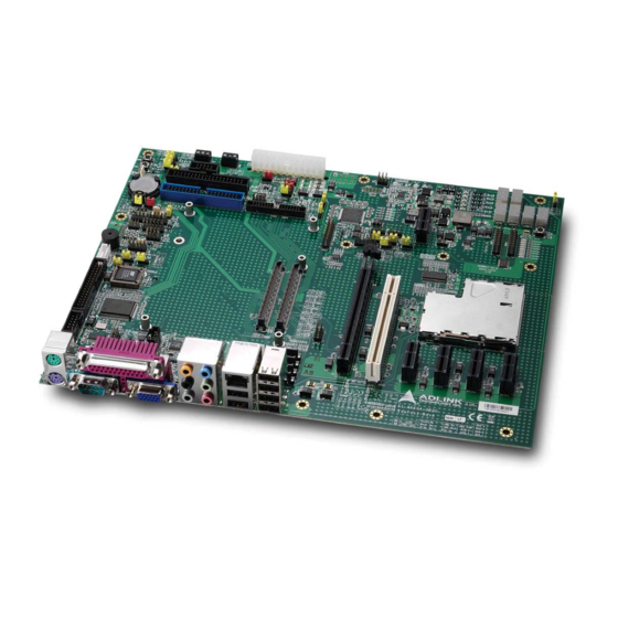
Page 9: Component Location
3 Component Location PCIE5 LEDX8 – X1 CNY2 PCIE4 CNY3 PCIE2 PCIE1 PCIE6 PCIE3 LED21 LED2 JPY4 PCI2 CN30 JPY5 LED20 JPY2 PCIE7 CN31 PWR_OK CNY1 CNZ1 CN32 CN21 CN41 CN13 JPY11 CN20 CNY5 CNY8 CNY4 CNY11 CN15 CN35 CNY9 CNY10 CN14 CN10... -
Page 10: Function Block Diagram
4 Function Block Diagram LPT1 COM1 W83627HG COM2 Primary Super I/O KB/MS Debug Header Secondary BIOS PCI Express PCI Express x16 POST Code onboard slot Graphics x16 Display 4 onboard SATA SATA headers ALC883 Audio on Codec Rear I/O Gigabit Onboard IDE Ethernet PATA... -
Page 11: Mechanical Dimensions
5 Mechanical Dimensions Express-BASE User’s Manual Page 11... -
Page 12: Connectors And Pin-Outs
6.2 Connector and Pin-out Compatibility Connectors positions and pin-outs comply with pin-out and signal description used in the original: “COM.0 - COM Express Module Base specification”. This document includes: description of pin- outs, signal descriptions and mechanical characteristics of the COM Express (Express) form factor. -
Page 13: Com Express Board-To-Board Connectors
6.3 COM Express Board-to-Board Connectors Signals and Pinout for: D110 C110 Basic form factor, Type 2. B110 A110 Row A Row B Row C Row D Pin No. Pin Name Pin No. Pin Name Pin No. Pin Name Pin No. Pin Name... - Page 14 COM Express Board-to-Board Connectors continued: Row A Row B Row C Row D Pin No. Pin Name Pin No. Pin Name Pin No. Pin Name Pin No. Pin Name VCC_RTC EXCD1_PERST# PCI_AD29 PCI_IRQD# EXCD0_PERST# EXCD1_CPPE# PCI_AD31 PCI_CLKRUN# EXCD0_CPPE# SYS_RESET# PCI_IRQA#...
-
Page 15: Pci Express And Pci Express Graphic (Peg) Slots
6.4 PCI Express and PCI Express Graphic (PEG) slots PCI Express x1: Signal Signal PCIE1 + 12V + 12V + 12V PCIE2 + 12V PCIE4 PCIE5 SMB_CK PCIE6 SMB_DAT + 3.3V TRST# + 3.3V +3.3VSB + 3.3V WAKE# PERST# REFCLK+ PETp0 REFCLK- PETn0... - Page 16 PCIE7: PCI Express x16 mode See the JP6 jumper description for PCI Express x16 mode and SDVO mode settings. Signal Signal Signal Signal PETn6 + 12V PERp6 + 12V + 12V PERn6 + 12V PETp7 PETn7 SMB_CK PERp7 SMB_DAT PERn7 + 3.3V PETp8 TRST#...
- Page 17 PCIE7: SDVO mode See the JP6 jumper description PCI Express x16 mode and SDVO mode settings. Signal Signal Signal Signal + 12V SDVOC_BLU- + 12V + 12V RSVD + 12V RSVD SDVOC_CK+ SMB_CK SDVOC_CK- SMB_DAT RSVD RSVD + 3.3V TRST# + 3.3V RSVD +3.3VSB...
-
Page 18: Pci Slots
6.5 PCI slots PCI interrupts OnboardDevice Pin INTA# Pin INTB# Pin INTC# Pin INTD# IDSEL PCI Slot 2 X1_INTB# X1_INTA# X1_INTD# X1_INTC# AD20 PCI2: 32-bit PCI slot (INTB#) Signal Signal Signal Signal TRST_L -12V AD[16] AD[17] +12V +3.3V C/BE[2]_L Ground FRAME_L Ground Ground... -
Page 19: Lpc Debug
6.6 LPC Debug CN32: LPC Debug header Signal Signal LPC_CLK LPC_FRAME# LPC_RST# + 5V LPC_AD3 LPC_AD2 + 3.3V L_AD1 LPC_AD0 SMB_CK SMB_DAT SPD_A1 (See JP3) 16 SPD_A0 (See JP4) LPC_SERIRQ KBRST# A20GATE# Signal Signal CNY1: LPC Test Connector LPC_DRQ0# LPC_AD0 (compatible with ADLINK LPC_DRQ1# LPC_AD1... -
Page 20: Usb And Lan
6.8 USB and LAN CN6: USB x4 Connector Signal USB- USB+ Ground CN7: RJ-45 Gbe LAN Signal + USB MDI[0]+ MDI[0]- MDI[1]+ MDI[1]- MDI[2]+ MDI[2]- MDI[3]+ MDI[3]- Signal USB- USB+ Ground CN13: USB Header Signal USB- USB+ Ground Page 20 Express-BASE User’s Manual... -
Page 21: Audio
6.9 Audio CN2: Six-in-One Color Signal BLUE Line-In Audio Phone Jack GREEN Line-Out PINK MIC-In ORANGE Center/Subwoofer BLACK Rear Speaker Out GRAY Side Speaker Out CN14: Audio Pin Header Signal Signal MIC-In-L AGND MIC-In-R ACZ Detect Line-In-R MIC-In Detect Front I/O Sense Line-In-L Line-In Detect CN8:... -
Page 22: Crt Vga, Lvds And Tv-Out
6.10 CRT VGA, LVDS and TV-out CN1: VGA CRT Signal Signal Green Blue DDC Power DDC2B Data HSYNC Vsync DDC2B clock CN27: TV-out header Signal Pin Signal S-Video: Luminance (Y) analog signal S-Video: Chrominance (C) analog signal Component video: Chrominance (Pb) analog signal CNY5: LVDS Flat Panel Connector Signal... -
Page 23: Keyboard & Mouse
CNY8: Backlight Control Signal Signal Panel PWR See JP7 and JP8 to set the Backlight CTRL Backlight Power voltage and Backlight Enable 6 Panel Power voltage. BLCTL Backlight PWR 6.11 Keyboard & Mouse CN4: Mouse (top) Signal MSDAT KB5V MSCLK Signal Keyboard (bottom) KBDAT... -
Page 24: Serial And Irda Ports
6.12 Serial and IrDA Ports Signal Signal CN3: COM1 DB9 DCD# RTS# CTS# DTR# Signal Signal CN18: COM2 Header DCD# RTS# CTS# DTR# CN24: IrDA Connector Signal No connect IrRXD Ground IrTXD 6.13 Parallel Ports CN5: DB25 Signal Signal STROBE# AUTOFD# DATA0 ERROR#... -
Page 25: Storage: Sata, Pata, Cf, Fdd
6.14 Storage: SATA, PATA, CF, FDD Signal Signal CN35: IDE Connector Reset IDE IDE Data 7 IDE Data 8 IDE Data 6 IDE Data 9 IDE Data 5 IDE Data 10 IDE Data 4 IDE Data 11 IDE Data 3 IDE Data 12 IDE Data 2 IDE Data 13... -
Page 26: Other Pin Headers
Speaker Keyboard Lock RESET RESET HDD LED HDD LED Power Button Power Button CN25: GPIO Header Signal Signal GPI0 GPO0 GPIOs of CN25 come from GPI1 GPO1 the COM Express module. GPI2 GPO2 GPI3 GPO3 Page 26 Express-BASE User’s Manual... - Page 27 CNY2-3: Digital I/O Signal Signal I/O 0 The Express-Base provides I/O 1 GPIO expansion for I²C I/O 2 applications via a Phillips I/O 3 PCA955 that provides a I/O 4 16-bit I²C I/O port with I/O 5 interrupt. I/O 6 I/O 7 INT# BATLOW#...
-
Page 28: Power Connectors
6.16 Power Connectors CN41: ATX Power Connector 24-pin +3.3 V +3.3 V -12 V +3.3 V Ground PWR_ON +5 V Ground +5 V Ground -5 V PWR_GOOD +5 V +5 V +5 V +12 V +5 V +12 V +3.3 V CN33: 12 Volt FAN Power Signal... - Page 29 CNY6: PWR_OK Config Jumper Status Add 3.3V Pullup with 10K to signal PWR_OK Jumper Connect PWRGOOD of ATX power supply <<<< Connect PWRGOOD of onboard DCDC regulator CNY7: Power Up Config Jumper Status 1-10 Jumper Power-up by module <<<< Power-up by Super I/O* *The Super I/O detects a power button event using the 'PSIN' pin.
-
Page 30: Jumper Settings
6.17 Jumper Settings JP1: LPC Port 80 Jumper Status Free Run <<<< Free Run: BIOS will complete the boot process Single Step Single Step: BIOS will execute step-by-step by pressing SW2 button JP2: BIOS Selection Jumper Status Enable <<<< Enable: Use the BIOS onboard module Disable Disable:... - Page 31 JP6: External PEG/Internal Graphics with SDVO Selection See also PCIE7: PCI Express x16 mode and SDVO mode. This jumper enables/disables Internal Graphics or external graphics on the x16 PCI Express Graphics (PEG) port. If the PEG port is enabled, both the Internal Graphics and SDVO will be disabled.
- Page 32 I2C/SMBus Buffers These buffers settings are for isolation of the I2C and SMBus - test feature only. ON : I2C/SMBus passes through LTC4300A-2 Buffer OFF : Bypass Buffer JPY2: I2C BUFFER (data) Jumper Status <<<< JPY3: I2C BUFFER (clock) Jumper Status <<<<...
- Page 33 JPY7, JPY8: Reserved JPY9: Backlight Enable Signal Type Jumper Status Inverse Sets the Backlight Enable Signal to "Normal" Normal <<<< or "Inverse" type. JPY10: PS_ON# Signal Source Jumper Status SUS_S3# <<<< All ADLINK modules support S3 mode and SUS_S5# consecutive power down of ATX power supply. For modules that connect the S3 signal, PS_ON# should always be set to SUS_S3# as source (even when S3 mode is disabled in the...
- Page 34 I2C EEPROM Address Selection JPY12 to JPY14 configure the address of the A0, A1 and A2 bits of the I2C EEPROM JPY12: I2C EEPROM A0 Jumper Status A0_HIGH "1" A0_LOW "0" <<<< JPY13: I2C EEPROM A1 Jumper Status A1_HIGH "1" A1_LOW "0"...
-
Page 35: Tips
7 Tips On/Off and RESET The top left corner of the board contains two mini switches. The SW3 switch is the ATX power button. This switch can be used to power up and power down the system with an ATX power supply. -
Page 36: Post Display
To the left of the POST display a column of 5 mini LEDs indicate what type of COM Ex- press module is installed on Express-BASE. COM Express type: 1-2, 3, 4, 5 or wrong pinout Indicator LEDs A row of mini LEDs to the left of the POST... -
Page 37: Digital I/O Leds
Digital I/O LEDs LEDX1 - LEDX8 are indicators for the Digital I/O Connector CNY2. When the I/O signal is high, the LED will light. The I/O 0 signal corresponds to LEDX1, and the I/O 7 signal corresponds to LEDX8. Express-BASE User’s Manual Page 37... -
Page 38: Important Safety Instructions
Important Safety Instructions For user safety, please read and follow all instructions, warnings, cautions, and notes marked in this manual and on the associated equipment before handling/operating the equipment. Read these safety instructions carefully. Keep this user’s manual for future reference. Read the specifications section of this manual for detailed information on the operating environment of this equipment. - Page 39 Equipment must be serviced by authorized technicians when: - The power cord or plug is damaged; - Liquid has penetrated the equipment; - It has been exposed to high humidity/moisture; - It is not functioning or does not function according to the user’s manual; - It has been dropped and/or damaged;...
-
Page 40: Getting Service
Address: 9F, No.166 Jian Yi Road, Chungho City, Taipei County 235, Taiwan Tel: +886-2-8226-5877 Fax: +886-2-8226-5717 Email: service@adlinktech.com Ampro ADLINK Technology Inc. Address: 5215 Hellyer Avenue, #110, San Jose, CA 95138, USA Tel: +1-408-360-0200 Toll Free: +1-800-966-5200 (USA only) Fax: +1-408-360-0222 Email: info@adlinktech.com... - Page 41 Address: 84 Genting Lane #07-02A, Cityneon Design Centre, Singapore 349584 Tel: +65-6844-2261 Fax: +65-6844-2263 Email: singapore@adlinktech.com ADLINK Technology Singapore Pte Ltd. (Indian Liaison Office) Address: No. 1357, "Anupama", Sri Aurobindo Marg, 9th Cross, JP Nagar Phase I, Bangalore - 560078, India Tel: +91-80-65605817 Fax: +91-80-22443548 Email: india@adlinktech.com...
Need help?
Do you have a question about the com express and is the answer not in the manual?
Questions and answers