
Related Manuals for ADLINK Technology COM Express nanoX-BASE


Summary of Contents for ADLINK Technology COM Express nanoX-BASE
- Page 1 nanoX-BASE User’s Manual Manual Revision: 2.02 Revision Date: September 2, 2013 Part Number: 50-1J030-1020...
- Page 2 Revision History Release Date Change 2.00 2010/10/19 Intial Release 2.01 2012/07/11 Add COM.0 R2.0 Type 10 module support (PCB rev. A2) 2.02 2013/09/02 Correct USB Client connector description (CN13 ) Page 2 nanoX-BASE User’s Manual...
-
Page 3: Table Of Contents
Table of Contents Preface ..........................5 1 Introduction ....................... 7 2 Special Features ....................... 9 Primary LPC based Super I/O....................9 Secondary BIOS ........................9 Onboard Audio ........................9 GPIO on Carrier ........................9 Information LEDs ........................9 Power, Reset, Lid and Sleep Switches ................. 9 3 Component Location .................... - Page 4 6.16 Keyboard & Mouse ......................28 6.17 Parallel Port ........................28 6.18 SATA ........................... 29 6.19 Smart Battery Management ....................29 6.20 Fans ............................ 29 6.21 GPIO ........................... 30 6.22 Other Connectors ........................ 31 6.23 Power Connectors ......................32 6.24 Power Jumper Settings .......................
-
Page 5: Preface
Preface Copyright 2010-13 ADLINK Technology, Inc. This document contains proprietary information protected by copyright. All rights are reserved. No part of this manual may be reproduced by any mechanical, electronic, or other means in any form without prior written permission of the manufacturer. - Page 6 Conventions Take note of the following conventions used throughout this manual to make sure that users perform certain tasks and instructions properly. Additional information, aids, and tips that help users perform tasks. Information to prevent minor physical injury, component damage, data loss, and/or program corruption when trying to complete a task.
-
Page 7: Introduction
1 Introduction The COM Express approach of custom carrier combined with off the shelf system cores is an excellent solution when you need to customize but lack the time or quantity for a complete redesign. It fits most system integration projects with production volumes from 500 to 10,000 pcs per year. - Page 8 Package Contents Before unpacking, check the shipping carton for any damage. If the shipping carton and/or contents are damaged, inform your dealer immediately. Retain the shipping carton and packing materials for inspection. Obtain authorization from the dealer before returning any product to ADLINK.
-
Page 9: Special Features
2 Special Features 2.1 Primary LPC based Super I/O COM Express modules do not have a Super I/O chip onboard as this is considered legacy. Therefore, a Super I/O is placed on the carrier board as an optional item. The nanoX-BASE equipped with a Winbond W83627DHG-P that supports LPT, COM and PS/2 keyboard/mouse. -
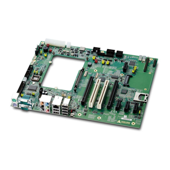
Page 10: Component Location
3 Component Location JP19 CN39 CN38 CN31 PCIE3 CN18 PCIE2 PCIE1 PCIE6 PCIE4 PCIE5 PCI2 CN10 CN32 PCI1 CN33 CN30 CN37 SDVO1 CN15 CN13 CNX5 JP24 CN21 CN12 CN14 CN28 CN41 CN26 CN24 CN23 CN35 CNX4 JP18 CNX3 JPX3 JPY7 CN21 CN15 SW1 SW2... -
Page 11: Function Block Diagram
4 Function Block Diagram USB0 USB1 4-port Single Channel LVDS Header USB3 Flat Panel Control Signals Header USB4 SDVO RJ-45 Flat cable in PCIe x16 Slot USB5 & 2-port SDVO Flat cable out (Type 10) USB2 Mini USB SATA0 USB6 SATA PCIe (x1) -
Page 12: Mechanical Dimensions
5 Mechanical Dimensions tolerances ± 0.05 mm Other tolerances ± 0.2 mm Page 12 nanoX-BASE User’s Manual... -
Page 13: Connectors And Pinouts
6 Connectors and Pinouts 6.1 Carrier Board Signals .125. .95. - Gigabit Ethernet port .84. - LPC interface - 4 Serial ATA channels - AC'97 or High Definition Audio - 6 USB 2.0 ports - 6 PCI Express x1 Lanes - Dual 24-bit LVDS channels - SDVO (Type 10) - TV-out, VGA (Type 1) -
Page 14: Com Express Board-To-Board Connector
6.4 COM Express Board-to-Board Connector Pinouts comply with B110 COM Express Type 1 and Type 10 A110 COM Express Type 1 COM Express Type 10 Row A Row B Row A Row B Pin No. Pin Name Pin No. Pin Name Pin No. - Page 15 COM Express Board-to-Board Connector (cont'd) COM Express Type 1 COM Express Type 10 Row A Row B Row A Row B Pin No. Pin Name Pin No. Pin Name Pin No. Pin Name Pin No. Pin Name A51 GND (FIXED) B51 GND (FIXED) A51 GND (FIXED) B51 GND (FIXED)
-
Page 16: Pci Express And Sdvo Slots
6.5 PCI Express and SDVO Slots PCI Express x1 Signal Signal PCIE1 + 12V + 12V + 12V PCIE2 + 12V PCIE3 PCIE6 SMB_CK SMB_DAT + 3.3V TRST# + 3.3V +3.3VSB + 3.3V WAKE# PERST# REFCLK+ PETp0 REFCLK- PETn0 PERp0 PERn0 PCI Express Mini Card - PCIE4 (USB6) Signal... - Page 17 PCI Express x16 (x1 mode) - PCIE5 Signal Signal Signal Signal + 12V + 12V + 12V + 12V SMB_CK SMB_DAT + 3.3V TRST# + 3.3V +3.3VSB + 3.3V WAKE# PERST# REFCLK+ PETp0 REFCLK- PETn0 PERp0 RSVD PERn0 nanoX-BASE User’s Manual Page 17...
- Page 18 SDVO from Module to Flat Cable connector CN30 Since COM Express Type 1 and Type 10 only define the AB connector, the CD connector which brings out SDVO signals from COM Express Type 2~6 modules to the carrier is not available. The method described below for connecting SDVO signals from the module to the carrier allows the nanoX-BASE to be compatible with both Type 1 and Type 10 modules.
- Page 19 SDVO (via Flat Cable connector CN30) - SDVO1 Signal Signal Signal Signal + 12V SDVOC_BLU- + 12V + 12V RSVD + 12V RSVD SDVOC_CK+ SMB_CK SDVOC_CK- SMB_DAT RSVD RSVD + 3.3V TRST# + 3.3V RSVD +3.3VSB + 3.3V RSVD WAKE# PERST# RSVD RSVD...
-
Page 20: Pci Slots
6.6 PCI Slots PCI Interrupts Onboard Device Pin INTA# Pin INTB# Pin INTC# Pin INTD# IDSEL PCI1 X1_INTA# X1_INTB# X1_INTC# X1_INTD# AD20 PCI2 X1_INTB# X1_INTC# X1_INTD# X1_INTA# AD21 PCI1, PCI2: 32-bit PCI Slots Signal Signal Signal Signal TRST_L -12V AD[16] AD[17] +12V +3.3V... -
Page 21: Lpc Debug
6.7 LPC Debug CN35: LPC Debug Header Signal Signal +3.3V LPC_AD3 BIOS_DIS0-L LPC_AD2 RST_DBG LPC_AD1 LPC_FRAME-L LPC_AD0 CLK_DEBUG 6.8 SD Card Slot Signal SD_DAT2 SD_DAT3 SD_CMD +3.3V SD_CLK SD_DAT0 SD_DAT1 See 6.21 GPIO - S1 for instructions on how to enable/disable the SD card slot. 6.9 SMBus (for user access) Signal... -
Page 22: I2C Bus
6.10 I C Bus (for user access) CN32: C Bus Signal I2C_DAT I2C_CK I2C EEPROM Address Selection Jumpers JP15 to JP17 configure the device address of the Atmel AT24C08A I2C EEPROM. JP15: I2C EEPROM A0 Jumper Status A0_HIGH "1" A0_LOW "0" <<<< JP16: I2C EEPROM A1 Jumper... -
Page 23: Usb And Lan
6.11 USB and LAN CN12: USB x4 Connector Signal USB- USB+ Ground Not Connected CN14: RJ-45 GbE LAN Signal + USB BI_DA+ BI_DA- BI_DB+ BI_DC+ BI_DC- BI_DB- BI_DD+ BI_DD Signal USB- USB+ Ground CN13: Mini-USB (USB Client) Signal Mini USB Mode This connector supports USB client USB- functionality using the Intel SCH USB... -
Page 24: Audio
6.12 Audio CN23: Audio Pin Header Signal Signal MIC-In-L AGND MIC-In-R ACZ Detect Line-In-R MIC-In Detect Front I/O Sense Line-In-L Line-In Detect CN24: CD Audio-out Connector Signal LINR AGND AGND LINL CN28: Six-in-One Color Signal BLUE Line-In Audio Phone Jack GREEN Line-Out PINK... -
Page 25: Lvds Panel Connectors
6.13 LVDS Panel Connectors CNY6: LVDS Flat Panel Connector Signal Signal LVDS_I2C_DAT LVDS_I2C_CK Panel_PWR Panel_PWR LVDS_A0- LVDS_A0+ LVDS_VDD_EN LVDS_A1- LVDS_A1+ LVDS_BKLT_EN LVDS_A2+ LVDS_A2- LVDS_A_CK- LVDS_A_CK+ Panel_PWR LVDS_A3+ LVDS_A3- Signal Signal CN7: Backlight Control Panel PWR Backlight CTRL Backlight Enable Backlight PWR See 6.14 LVDS Jumper Settings for Panel Power Voltage (JP3), Backlight Power Voltage (JP4) and other LVDS jumper settings. -
Page 26: Lvds Panel Jumpers
6.14 LVDS Panel Jumpers JP3: Panel Power Voltage Jumper Status +3.3V <<<< Selects the Panel PWR voltage on CN7 Backlight Control pin header (pin 2). JP4: Backlight Power Voltage Jumper Status +12V Selects the Backlight PWR voltage on <<<< CN7 Backlight Control pin header (pin 8). JP20: Brightness Control Jumper... -
Page 27: Serial And Irda Ports
6.15 Serial and IrDA Ports Signal Signal CNX1/2: COM1/2 From Type 10 Module. CNX4: COM1 (top) Signal Signal DCD# COM2 (bottom) RTS# From Super I/O on nanoX-BASE. CTS# DTR# CN20: IrDA Connector Signal From Super I/O on nanoX-BASE. No connect IrRXD Ground IrTXD... -
Page 28: Keyboard & Mouse
6.16 Keyboard & Mouse Signal CN15: Mouse (top) MSDAT KB5V MSCLK Signal Keyboard (bottom) KBDAT KB5V KBCLK 6.17 Parallel Port Signal Signal CN17: DB25 STROBE# AUTOFD# Pin defintion is for the LPT DATA0 ERROR# IDC to DB25 cable DATA1 INIT# DATA2 SELIN# DATA3... -
Page 29: Sata
6.18 SATA CN8: SATA0 Signal Signal CN10: SATA1 6.19 Smart Battery Management CN37: BattMan Connector Signal Signal SMB_CLK SMB_DAT ADLINK BattMan board and PWRBTN BATLOW related cables are required for PS_ON +3.3V Smart Battery Management on +12V the nanoX-BASE carrier board. SMB_ALERT 6.20 Fans FN1-3:... -
Page 30: Gpio
6.21 GPIO CN39: Module GPIO Signal Signal GPI0 GPO0 GPIOs of CN39 come from GPI1 GPO1 the COM Express module. GPI2 GPO2 GPI3 GPO3 CN38: Carrier GPIO Signal Signal GPI0 GPO0 GPIOs of CN38 come from GPI1 GPO1 the NXP PCA9535 I/O Port GPI2 GPO2 onboard the nanoX-BASE... -
Page 31: Other Connectors
6.22 Other Connectors Signal Signal CN31: Miscellaneous Power LED BUZZER Connector WDT_LED SYS_RESET ATA_ACT PS_ON +3.3V 5V STB PWR_BTN SIO_PME CN18: Feature Connector Signal Signal +5VSB Hard Disk Activity I2C_DAT SMBCLK_SB I2C_CK SMBDATA_SB Internal use GPO0 Internal use GPO1 PS_ON# GPO2 SUS_S3# GPO3... -
Page 32: Power Connectors
6.23 Power Connectors CN1: ATX 24-pin Connector +3.3 V +3.3 V -12 V +3.3 V Connect the ATX 24-pin (or 20-pin) connector Ground to supply power to the nanoX-BASE carrier. PWR_ON +5 V Ground +5 V Ground -5 V PWR_GOOD +5 V +5 V +5 V... -
Page 33: Power Jumper Settings
6.24 Power Jumper Settings JP1: ATX/AT Mode Jumper Status ATX mode <<<< In AT mode, JP1 shorts PS_ON# to AT mode ground directly to force power on. JPX2: AT Power 5V Setting Jumper Status AT without P5V <<<< With an AT power supply is connected to AT with P5V the nanoX-BASE, JPX2 can be used to provide 5VSB to the COM module from... -
Page 34: Other Jumper Settings
6.25 Other Jumper Settings JP2: Clear CMOS Jumper Status Normal <<<< To clear CMOS, shut down the power and Clear CMOS short pins 2 and 3 (shorts VBAT to ground). JP6: Super I/O Address Jumper Status Selects the address of the Super I/O. <<<<... -
Page 35: Secondary Bios
7 Secondary BIOS The nanoX-BASE supports Secondary BIOS using firmware hub (FWH) for COM.0 Rev. 1.0 modules and Serial Peripheral Interface (SPI) for COM.0 Rev. 2.0 modules. Secondary BIOS solutions can be used as an alternative to the on-module BIOS and provide support for the following: Testing new BIOS versions Development of firmware modifications... -
Page 36: Spi Secondary Bios - Com.0 Rev. 2.0
SPI Secondary BIOS - COM.0 Rev. 2.0 SPI is supported by PICMG COM.0 Rev. 2.0 to provide a Secondary BIOS for COM Express Rev 2.0 modules that support a SPI Secondary BIOS. When using SPI Secondary BIOS, the FWH BIOS chip must be removed from the carrier board. -
Page 37: Switches, Leds & Power
8 Switches, LEDs & Power 8.1 Mini Switches (SW1~4) There are two mini switches at the top left corner of the board. The SW1 switch is the ATX Power Button. This switch can be used to power up and power down the system with an ATX power supply. -
Page 38: Post Display
8.2 POST Display An LPC-based POST display is provided for debugging. There are two LEDs that display the actual POST data. 8.3 Information LEDs A row of mini LEDs to the left of the POST display indicates the following: LED1 HDD: SATA hard disk activity LED2 5Vsb: ATX power on standby or active LED3 WDT: programmable LED to debug... -
Page 39: Atx Power Connectors
8.4 ATX Power Connectors The nanoX-BASE has one ATX 24-pin connector to supply power to the carrier board and one ATX 12V 4-pin connector to supply power to the COM Express module. ATX 24-pin ATX 12V 4-pin Connector Connector The system will not power on unless an ATX 12V 4-pin connector is connected. -
Page 40: At Power Mode
8.5 AT Power Mode To operate the system in AT Mode with an ATX power supply, use the AT mode PSU converter cable (no 5Vsb) to connect the ATX 20/24-pin power connector to the carrier board as shown. Set the ATX/AT Mode jumper JP1 to AT Mode as described in 6.24 Power Jumper Settings. Page 40 nanoX-BASE User’s Manual... -
Page 41: Important Safety Instructions
Important Safety Instructions For user safety, please read and follow all instructions, warnings, cautions, and notes marked in this manual and on the associated equipment before handling/operating the equipment. Read these safety instructions carefully. Keep this user’s manual for future reference. Read the specifications section of this manual for detailed information on the operating environment of this equipment. -
Page 42: Getting Service
5215 Hellyer Avenue, #110, San Jose, CA 95138, USA Tel: +1-408-360-0200 Toll Free: +1-800-966-5200 (USA only) Fax: +1-408-360-0222 Email: info@adlinktech.com ADLINK Technology (China) Co., Ltd. Address: (201203) 300 Fang Chun Rd., Zhangjiang Hi-Tech Park, Pudong New Area, Shanghai, 201203 China Tel: +86-21-5132-8988 Fax:... - Page 43 84 Genting Lane #07-02A, Cityneon Design Centre, Singapore 349584 Tel: +65-6844-2261 Fax: +65-6844-2263 Email: singapore@adlinktech.com ADLINK Technology Singapore Pte. Ltd. (Indian Liaison Office) Address: 1st Floor, #50-56 (Between 16th/17th Cross) Margosa Plaza, Margosa Main Road, Malleswaram, Bangalore-560055, India Tel: +91-80-65605817, +91-80-42246107 Fax: +91-80-23464606 Email: india@adlinktech.com...
Need help?
Do you have a question about the COM Express nanoX-BASE and is the answer not in the manual?
Questions and answers