
Subscribe to Our Youtube Channel
Related Manuals for ADLINK Technology cPCI-R6500 Series


Summary of Contents for ADLINK Technology cPCI-R6500 Series
- Page 1 cPCI-R6500 6U CompactPCI® Rear Transition Module MXM Graphics Carrier User’s Manual Manual Rev.: 0.10 Preliminary Revision Date: October 23, 2015 Part No: 50-15084-1000 Advance Technologies; Automate the World.
- Page 2 Revision History Revision Release Date Description of Change(s) 0.10 2015/10/23 Preliminary release Revision History...
-
Page 3: Preface
Preface Copyright 2015 ADLINK Technology, Inc. This document contains proprietary information protected by copy- right. All rights are reserved. No part of this manual may be repro- duced by any mechanical, electronic, or other means in any form without prior written permission of the manufacturer. - Page 4 Conventions Take note of the following conventions used throughout this manual to make sure that users perform certain tasks and instructions properly. Additional information, aids, and tips that help users perform tasks. NOTE: NOTE: Information to prevent minor physical injury, component dam- age, data loss, and/or program corruption when trying to com- plete a task.
-
Page 5: Table Of Contents
Board Layout........... 7 cPCI-R6500D Assembly Layout .......... 8 cPCI-R6501D Assembly Layout .......... 9 cPCI-R65N0 Assembly Layout .......... 10 cPCI-R6500 Series Faceplate ........... 11 Connector Pin Assignments ..........12 Switch Settings ..............22 Important Safety Instructions ..........25 Getting Service..............27... - Page 6 This page intentionally left blank. Table of Contents...
-
Page 7: List Of Figures
Figure 3-1: cPCI-R6500 Board Layout - Component Side....7 Figure 3-2: cPCI-R6500D Assembly Layout ........8 Figure 3-3: cPCI-R6501D Assembly Layout ........9 Figure 3-4: cPCI-R65N0 Assembly Layout ........10 Figure 3-5: cPCI-R6500 Series Faceplate ........11 List of Figures... - Page 8 This page intentionally left blank. viii List of Figures...
-
Page 9: List Of Tables
cPCI-R6500 List of Tables Table 2-1: cPCI-R6500(D) I/O Connectivity........6 Table 3-1: DVI-I Connector Pin Definition........12 Table 3-2: DVI-I Connector Pin Definition........13 Table 3-3: CompactPCI J3 Connector Pin Definition...... 20 Table 3-4: CompactPCI J5 Connector Pin Definition...... 21 Table 3-5: COM2 Mode Switch Settings......... - Page 10 This page intentionally left blank. List of Tables...
-
Page 11: Introduction
Introduction 1.1 Overview The cPCI-R6500 Series is 6U CompactPCI rear transition module (RTM) designed for use with ADLINK 6U CompactPCI CPU blades. The cPCI-R6500 is an RTM equipped with an ATI or NVIDIA MXM graphics module to provide additional graphics per- formance for embedded applications and supports comprehensive rear I/O functionality. -
Page 12: Features
1.2 Features 6U CompactPCI RTM in 8HP width form factor Compliant with CompactPCI Specification 2.0, Rev. 3.0 Compliant with CompactPCI Packet Switching Backplane Specification PICMG 2.16 Rev. 1.0 64-bit/66 MHz CompactPCI interface based on PCI specifica- tions Realtek ALC262 HD Audio codec and Mic-in, Line-in, Line-out via onboard 10-pin audio box header Two DVI-I ports for dual independent displays (MXM graphics module dependent) -
Page 13: Block Diagram
cPCI-R6500 1.3 Block Diagram PCIE x4 MXM 3.0 DVI-I DVI-I SATA 0 SATA 7-pin connector RS-232/422/485 10-pin box header DB-9 USB x1 LAN x2 (PICMG 2.16) PS/2 KB/MS PS/2 KB/MS PS/2 KB/MS 10-pin header KB/MS USB x2 USB x2 10-pin header TX, RX, GND RS-232 10-pin box header SATA 1/2... -
Page 14: Package Contents
Please obtain authorization before returning any product to ADLINK. cPCI-R6500 Series MXM carrier MXM graphics module, model dependent on model selected (installed) 2.5" drive bracket kit (cPCI-R6501D only) -
Page 15: Specifications
cPCI-R6500 Specifications 2.1 cPCI-R6500 General Specifications Standards • CompactPCI® Specification 2.0, Rev. 3.0 • CompactPCI® Packet Switching Backplane Specification PICMG 2.16 Rev. 1.0 Form Factor • Standard 6U CompactPCI® Rear Transition Module • Board size: 233.35mm x 80mm • Dual-slot (8HP, 40.64mm) •... -
Page 16: I/O Connectivity
Environmental • Operating Temperature: 0 °C to +60 °C • Extended Temperature: -20 °C to +70 °C (by screening) Figure 2-1: cPCI-R6500 Series General Specifications 2.2 I/O Connectivity cPCI-R6500D cPCI-R6501D cPCI-R65N0 Function Faceplate Board Faceplate Board Faceplate Board Y x2... -
Page 17: Board Interfaces
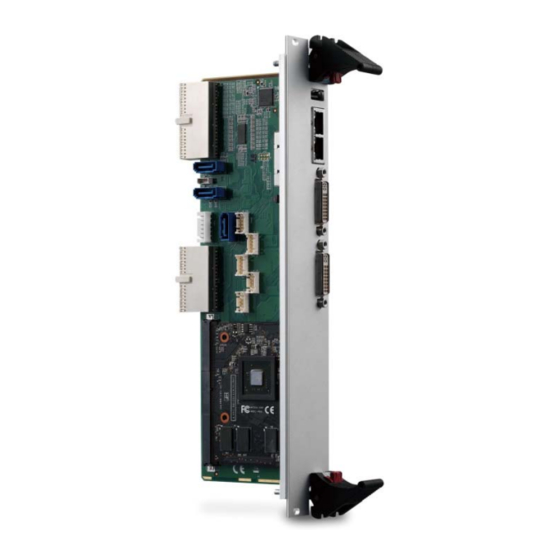
cPCI-R6500 Board Interfaces This chapter illustrates the board layout, connector pin assignments, and switch settings to familiarize users with the cPCI-R6500. 3.1 cPCI-R6500 Board Layout CN10 COM2 USB1 HDA1 COM1 PS/1 rJ1/2 CompactPCI connectors COM1/2 Serial port box header MXM connector HDA1 Audio box header CN4/5/6 SATA connectors... -
Page 18: Cpci-R6500D Assembly Layout
3.2 cPCI-R6500D Assembly Layout DVI-D PS/2 KB/MS DVI-I MXM Thermal Module Figure 3-2: cPCI-R6500D Assembly Layout Board Interfaces... -
Page 19: Cpci-R6501D Assembly Layout
cPCI-R6500 3.3 cPCI-R6501D Assembly Layout 2.5” SATA Drive DVI-D DVI-I MXM Thermal Module Figure 3-3: cPCI-R6501D Assembly Layout Board Interfaces... -
Page 20: Cpci-R65N0 Assembly Layout
3.4 cPCI-R65N0 Assembly Layout DVI-D PS/2 KB/MS DVI-I MXM Thermal Module Figure 3-4: cPCI-R65N0 Assembly Layout Board Interfaces... -
Page 21: Cpci-R6500 Series Faceplate
3.5 cPCI-R6500 Series Faceplate cPCI-R6500D PS/2 KB/MS DVI-I DVI-D a LAN b cPCI-R6501D DVI-I DVI-D a LAN b cPCI-R65N0 PS/2 KB/MS DVI-I DVI-D a LAN b Figure 3-5: cPCI-R6500 Series Faceplate Board Interfaces... -
Page 22: Connector Pin Assignments
3.6 Connector Pin Assignments Faceplate Connectors DVI-I Connectors Pin # Signal Pin # Signal TMDS Data2- Hot Plug Detect TMDS Data2+ TMDS Data0- TMDS Data2/4 Shield TMDS Data0+ TMDS Data4- TMDS Data0/5 Shield TMDS Data4+ TMDS Data5- DDC Clock [SCL] TMDS Data5+ DDC Data [SDA] TMDS Clock Shield... -
Page 23: Table 3-2: Dvi-I Connector Pin Definition
cPCI-R6500 DVI-D Connectors Pin # Signal Pin # Signal DVI_D_DAN2 DVI_D_HPD_L DVI_D_DAP2 DVI_D_DAN0 DVI_D_DAP0 DDCCLK_D DDCDATA_D DVI_D_CLKP DVI_D_DAN1 DVI_D_CLKN DVI_D_DAP1 DVI_D_5V Table 3-2: DVI-I Connector Pin Definition USB 2.0 Type A Connectors Pin # Signal Name USB_D- USB_D+ Board Interfaces... - Page 24 LAN Connectors (RJ-45) 10BASE-T/ Pin # 1000BASE-T 100BASE-TX LAN_TXP0 LAN_TXN0 LAN_TXP1 LAN_TXP2 LAN_TXP2 Speed Activity LAN_TXN1 LAN_TXP3 LAN_TXN3 Speed LED Activity LED Status (Green/Amber) (Amber) Network link is not established or system powered off Link 10 Mbps Active Blinking Link Green 100 Mbps Active...
- Page 25 cPCI-R6500 COM2 RS-232/422/485 Connector Pin # RS-232 RS-422 RS-485 TXD- Data- TXD+ Data+ RXD+ See “COM2 Mode Switches (SW1)” on page 22. NOTE: NOTE: PS/2 Keyboard/Mouse Port (cPCI-R6500D/R65N0 only) Pin # Signal Function KB_DATA Keyboard Data MS_DATA Mouse Data Ground KM_VCC Power KB_CLK...
- Page 26 Onboard Connectors SATA Connectors (CN4/5/6) Pin # Signal Auxiliary Power Connector (CN3) (6-pin, 2.5 mm pitch Wafer - use with cable PN: 30-20077-2000) Pin # Signal P12V P12V SATA Power Connector (CN10) (5-pin, 1.25 mm pitch Wafer) Pin # Signal P12V Board Interfaces...
- Page 27 cPCI-R6500 COM1 Box Header (RS-232 RX/TX only) (2x5-pin, 2.0 mm pitch Wafer) Pin # RS-232 Signal COM2 Box Header (RS-232/422/485) (2x5-pin, 2.0 mm pitch Wafer) Pin # RS-232 RS-422 RS-485 TXD- Data- TXD+ Data+ RXD+ RXD- Board Interfaces...
- Page 28 Fan Power Connector (CN9) Pin # Signal P12V Audio Box Header (HDA1) (2x5-pin, 2.0 mm pitch Wafer) Pin # Signal Pin # Signal L_OUT_L L_OUT_R L_IN_L L_IN_R MIC_LR PS/2 Keyboard/Mouse Box Header (PS/2) (2x5-pin, 2.0 mm pitch Wafer) Pin # Signal Pin # Signal...
- Page 29 cPCI-R6500 USB Box Header (USB1) (2x5-pin, 2.0 mm pitch Wafer) Pin # Signal Pin # Signal USB4_D- USB7_D- USB4_D+ USB7_D+ Board Interfaces...
-
Page 30: Table 3-3: Compactpci J3 Connector Pin Definition
CompactPCI rJ3 Pin Assignment Pin Z 19 GND P12V 18 GND LAN2_TXP0 (b) LAN2_TXN0 (b) LAN2_TXP2 (b) LAN2_TXN2 (b) GND 17 GND LAN2_TXP1 (b) LAN2_TXN1 (b) LAN2_TXP3 (b) LAN2_TXN3 (b) GND 16 GND LAN1_TXP0 (a) LAN1_TXN0 (a) LAN1_TXP2 (a) LAN1_TXN2 (a) GND 15 GND LAN1_TXP1 (a) LAN1_TXN1 (a) LAN1_TXP3 (a) LAN1_TXN3 (a) GND 14 GND... -
Page 31: Table 3-4: Compactpci J5 Connector Pin Definition
cPCI-R6500 CompactPCI rJ5 Pin Assignment LAN1_LINK_ LAN2_LINK_ ACT_L (a) ACT_L (b) SATA_RXP0 SATA_RXN0 SATA_TXP0 SATA_TXN0 LAN1_100-L (a) LAN2_100-L (b) LAN2_1G-L (b) LAN1_1G-L (a) BAT_RTM PCIE_CLKP PCIE_CLKN PLTRST-L PCIE_TXP4 PCIE_TXN4 PCIE_RXP4 PCIE_RXN4 PCIE_TXP3 PCIE_TXN3 PCIE_RXP3 PCIE_RXN3 PCIE_TXP2 PCIE_TXN2 PCIE_RXP2 PCIE_RXN2 PCIE_TXP1 PCIE_TXN1 PCIE_RXP1 PCIE_RXN1... -
Page 32: Switch Settings
3.7 Switch Settings COM2 Mode Switches (SW1) The COM2 serial port supports RS-232/422/485 modes. Switch SW1 can be used to configure the COM2 port to the desired mode using the settings shown below (set to RS-232 by default). Serial port mode RS-232 1 ON, 2 OFF RS-485... -
Page 33: Table 3-6: Lan Control Switch Settings
cPCI-R6500 LAN Control Switches (SW2, SW3) The cPCI-R6500 can route LAN signals from the CPU blade to either the PICMG 2.16 backplane or to LAN a/b on the face- plate I/O (but not both simultaneously). Switch SW2 can be used to route the LAN “a” signals and (set to faceplate RJ-45 connectors by default). - Page 34 This page intentionally left blank. Board Interfaces...
-
Page 35: Important Safety Instructions
cPCI-R6500 Important Safety Instructions For user safety, please read and follow all instructions, WARNINGS, CAUTIONS, and NOTES marked in this manual and on the associated equipment before handling/operating the equipment. Read these safety instructions carefully. Keep this user’s manual for future reference. Read the specifications section of this manual for detailed information on the operating environment of this equipment. - Page 36 Never attempt to fix the equipment. Equipment should only be serviced by qualified personnel. A Lithium-type battery may be provided for uninterrupted, backup or emergency power. Risk of explosion if battery is replaced with one of an incorrect type. Dispose of used batteries appropriately. WARNING: Equipment must be serviced by authorized technicians when:...
-
Page 37: Getting Service
5215 Hellyer Avenue, #110, San Jose, CA 95138, USA Tel: +1-408-360-0200 Toll Free: +1-800-966-5200 (USA only) Fax: +1-408-360-0222 Email: info@adlinktech.com ADLINK Technology (China) Co., Ltd. Address: (201203) 300 Fang Chun Rd., Zhangjiang Hi-Tech Park, Pudong New Area, Shanghai, 201203 China Tel: +86-21-5132-8988 Fax:... - Page 38 84 Genting Lane #07-02A, Cityneon Design Centre, Singapore 349584 Tel: +65-6844-2261 Fax: +65-6844-2263 Email: singapore@adlinktech.com ADLINK Technology Singapore Pte. Ltd. (Indian Liaison Office) Address: 1st Floor, #50-56 (Between 16th/17th Cross) Margosa Plaza, Margosa Main Road, Malleswaram, Bangalore-560055, India Tel: +91-80-65605817, +91-80-42246107 Fax: +91-80-23464606 Email: india@adlinktech.com...
Need help?
Do you have a question about the cPCI-R6500 Series and is the answer not in the manual?
Questions and answers