
Subscribe to Our Youtube Channel
Related Manuals for ADLINK Technology cExpress-EL


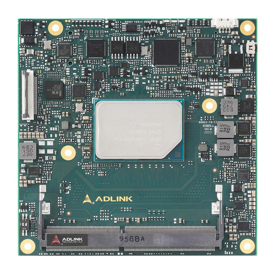
Summary of Contents for ADLINK Technology cExpress-EL
- Page 1 User’s Guide Revision: Rev. 1.1 Date: 2021-08-11 Part Number: 50M-00026-1010...
-
Page 2: Preface
Product names mentioned herein are used for identification purposes only and may be trademarks / registered trademarks of respective companies. Copyright © 2021 ADLINK Technology Incorporated This document contains proprietary information protected by copyright. All rights are reserved. No part of this manual may be reproduced by any mechanical, electronic, or other means in any form without prior written permission of the manufacturer. - Page 3 Only install/attach and operate equipment on stable surfaces and/or recommended mountings; • If the equipment will not be used for long periods of time, turn off the power source and unplug the equipment. • Page 2 Copyright © 2021 ADLINK Technology, Inc.
- Page 4 Caution: This information indicates the possibility of minor physical injury, component damage, data loss, and/or program corruption. Warning: This information warns of possible serious physical injury, component damage, data loss, and/or program corruption. Page 3 Copyright © 2021 ADLINK Technology, Inc.
- Page 5 User’s Guide PICMG COM.0 R3.0 Revision History Revision Description Date Author Initial release 2021-06-03 Update specs, mechanical drawings 2021-08-11 Page 4 Copyright © 2021 ADLINK Technology, Inc.
-
Page 6: Table Of Contents
4.3.1 Audio ..................................................................23 4.3.2 Analog VGA................................................................24 4.3.3 LVDS or eDP...............................................................25 4.3.4 Gigabit Ethernet ...............................................................28 4.3.5 SATA ..................................................................29 4.3.6 PCIe ..................................................................30 4.3.7 LPC Bus ................................................................32 4.3.8 USB..................................................................33 4.3.9 SPI Bus (BIOS only) ............................................................34 Page 5 Copyright © 2021 ADLINK Technology, Inc. - Page 7 7.1.3 Ubuntu.................................................................63 7.1.4 VxWorks 64-bit ..............................................................63 8. Mechanical and Thermal........................................................64 Module Dimensions ..............................................................64 Thermal Solutions ................................................................65 8.2.1 Heatspreader: HTS............................................................65 8.2.2 Heatsink: THS ..............................................................66 8.2.3 Heatsink: THSH ..............................................................67 8.2.4 Active Cooling: THSF ............................................................68 Page 6 Copyright © 2021 ADLINK Technology, Inc.
-
Page 8: List Of Figures
Figure 4 –COM Express® Compact Size Module and Debug Module ........................................54 Figure 5 – Module Dimensions .........................................................64 Figure 6 – Heatspreader HTS-cEL-I ......................................................65 Figure 7 – Heatsink THS-cEL-B-I.......................................................66 Figure 8 – Heatsink THSH-cEL-B-I ......................................................67 Figure 9 – Heatsink THSH-cEL-B-I ......................................................68 Page 7 Copyright © 2021 ADLINK Technology, Inc. -
Page 9: Introduction
Warning: This is an EA (early available) engineering manual. The contents may not accurately reflect the actual or final version of this product. The cExpress-EL is the first COM Express® COM.0 R3.0 Compact Size Type 6 module featuring the IT/OT convergence 6th Generation Intel Atom®... -
Page 10: Specifications
Note: SKUs supporting Intel® TCC paired with specific LAN solutions can also support TSN (TBC). Pentium, Celeron and some of Atom SKUs supported by project basis only. Please contact your local ADLINK presentative. Page 9 Copyright © 2021 ADLINK Technology, Inc. -
Page 11: Video
(eDP optional in place of LVDS, VGA optional in place of DDI 2) Encode/transcode HD content Playback of high definition content, including Blu-ray Disc and Blu-ray Disc 3D, using HDMI (1.4a spec compliant with 3D) Intel® QuickSync and Intel® Clear Video HD Page 10 Copyright © 2021 ADLINK Technology, Inc. -
Page 12: Display Interface Support
DDI x 2: Digital Display Ports (DDI) support DisplayPort 1.4, HDMI 1.4b or DVI VGA: VGA support, in place of DDI 2, max. resolution is 1920x1200@60Hz 2.3 Audio Intel® HD Audio integrated Located on carrier Express-BASE6 (ALC886 standard support) Page 11 Copyright © 2021 ADLINK Technology, Inc. -
Page 13: Expansion Busses
SuperSpeedPlus, SuperSpeed, High-Speed, Full-Speed and Low-Speed USB signalling Note: Carrier board must be designed for Gen2 operation. UART/CAN Two UART interfaces SER0 and SER1 RX/TX on Module Console Redirection COM 1 or COM 2 selectable in BIOS Page 12 Copyright © 2021 ADLINK Technology, Inc. - Page 14 Real-time I/O (under planning, TBC) 8x GPIO, I2C, 2x UART are BIOS configurable and managed by ARM Cortex M7 core for real-time applications Note: The above interfaces are BOM options and supported by project basis Page 13 Copyright © 2021 ADLINK Technology, Inc.
-
Page 15: Trusted Platform Module (Tpm)
Power States: C1-C6, S0, S1, S3, S4, S5, S5 ECO mode (Wake-on-USB S3/S4, WoL S3/S4/S5) ECO Mode support for deep S5 for 5Vsb power saving Power Consumption Please contact your ADLINK representative for the document “COM Express Module Power Consumption”. Page 14 Copyright © 2021 ADLINK Technology, Inc. -
Page 16: Mechanical And Environmental
Shock and Vibration IEC 60068-2-64 and IEC-60068-2-27 MIL-STD-202F, Method 213B, Table 213-I, Condition A and Method 214A, Table 214-I, Condition D HALT tested Thermal Stress, Vibration Stress, Thermal Shock and Combined Test Page 15 Copyright © 2021 ADLINK Technology, Inc. -
Page 17: Block Diagram
DDR4 SODIMM (top side) GPIO/SDIO (SoC) 3200 MT/s, non-ECC/IBECC Embedded Controller UART 0-1 Thermal sensor DDR4 SODIMM (bottom side) (board) 3200 MT/s, non-ECC/IBECC eSPI to LPC Figure 1 – Module Function Block Diagram Page 16 Copyright © 2021 ADLINK Technology, Inc. -
Page 18: Pinout And Signal Descriptions
The below table is a comprehensive list of all signal pins supported on the dual 220-pin COM Express connectors as defined for Type 6 in the PICMG COM.0 Rev 3.0 specification. Signals described in the specification but not supported on the cExpress-EL are marked by strikethrough STRIKETHROUGH A110 Figure 2 –... - Page 19 AC/HDA_SYNC AC/HDA_SDIN1 DDI1_PAIR5+ DDI1_PAIR1+ AC/HDA_RST# AC/HDA_SDIN0 DDI1_PAIR5- DDI1_PAIR1- GND (FIXED) GND (FIXED) GND (FIXED) GND (FIXED) AC/HDA_BITCLK SPKR DDI2_CTRLCLK_AUX+ DDI1_PAIR2+ AC/HDA_SDOUT I2C_CK DDI2_CTRLDATA_AUX- DDI1_PAIR2- BIOS_DIS0#/ESPI_SAFS* I2C_DAT DDI2_DDC_AUX_SEL DDI1_DDC_AUX_SEL THRMTRIP# THRM# RSVD RSVD Page 18 Copyright © 2021 ADLINK Technology, Inc.
- Page 20 RSVD RSVD PCIE_TX1+ PCIE_RX1+ RSVD RSVD PCIE_TX1- PCIE_RX1- PEG_RX4+ PEG_TX4+ WAKE0# PEG_RX4- PEG_TX4- GPI2 WAKE1# RAPID_SHUTDOWN PCIE_TX0+ PCIE_RX0+ PEG_RX5+ PEG_TX5+ PCIE_TX0- PCIE_RX0- PEG_RX5- PEG_TX5- GND (FIXED) GND (FIXED) GND (FIXED) GND (FIXED) Page 19 Copyright © 2021 ADLINK Technology, Inc.
- Page 21 A101 SER1_TX/CAN_TX * B101 FAN_PWMOUT C101 PEG_RX15+ D101 PEG_TX15+ A102 SER1_RX/CAN_RX * B102 FAN_TACHIN C102 PEG_RX15- D102 PEG_TX15- A103 LID# B103 SLEEP# C103 D103 A104 VCC_12V B104 VCC_12V C104 VCC_12V D104 VCC_12V Page 20 Copyright © 2021 ADLINK Technology, Inc.
- Page 22 USB 3.2 upgrade signals (lanes 2, 3) via USB Hub are BOM options supported by project basis eDP (in place of LVDS) and VGA (in place of DDI 2) are BOM options supported by project basis Page 21 Copyright © 2021 ADLINK Technology, Inc.
-
Page 23: Signal Terminology Descriptions
Pull-down strap. A Module output pin that is either tied to GND or is not connected. Used to signal Module capabilities to the Carrier Board. PU (pull-up) resistor on module PD (pull-down) resistor on module Page 22 Copyright © 2021 ADLINK Technology, Inc. -
Page 24: Ab Connector Signal Descriptions
Serial TDM data output to the CODEC. O 3.3V HDA_SDOUT AC_SDIN[2:0] / B28- B30 Serial TDM data inputs from up to 3 CODECs. B28 Not supported HDA_SDIN[2:0] 3.3VSB Elkhart Lake platform doesn’t offer AC_SDIN2/HDA_SDIN2 Page 23 Copyright © 2021 ADLINK Technology, Inc. -
Page 25: Analog Vga
I/O OD 3.3V PU 2k2 3.3V monitor capabilities) VGA_I2C_DAT DDC data line. I/O OD 3.3V PU 2k2 3.3V Note: VGA (in place of DDI 2) is BOM option supported by project basis Page 24 Copyright © 2021 ADLINK Technology, Inc. -
Page 26: Lvds Or Edp
LVDS_B0- LVDS_B1+ LVDS_B1- LVDS_B2+ LVDS_B2- LVDS_B3+ LVDS_B3- LVDS_B_CK+ LVDS_B_CK- LVDS_VDD_EN eDP_VDD_EN LVDS_BKLT_EN eDP_BKLT_EN LVDS_BKLT_CTRL eDP_BKLT_CTRL LVDS_I2C_CK eDP_AUX+ LVDS_I2C_DAT eDP_AUX- eDP_HPD Note : LVDS is default mode and eDP is a BOM option Page 25 Copyright © 2021 ADLINK Technology, Inc. - Page 27 PD 100K LVDS_I2C_CK DDC lines used for flat panel detection and control. O 3.3V PU 2k2 3.3V LVDS_I2C_DAT DDC lines used for flat panel detection and control. I/O 3.3V PU 2k2 3.3V Page 26 Copyright © 2021 ADLINK Technology, Inc.
- Page 28 I/O PCIE AC coupled off module eDP_HPD Detection of Hot Plug / Unplug and notification of the I 3.3V PD 100K PD 100K on this pin when eDP is supported link layer Page 27 Copyright © 2021 ADLINK Technology, Inc.
-
Page 29: Gigabit Ethernet
Gigabit Ethernet Controller 0 Software-Definable Pin. Can also be used for IO 3.3VSB GBE0_SDP IEEE1588 support such as 1pps signal. Note : 2.5GbE support by project basis (TBC). TSN supported by Linux OS. Page 28 Copyright © 2021 ADLINK Technology, Inc. -
Page 30: Sata
ATA (parallel and serial) or SAS activity indicator, active low. O 3.3V PU 10K 3.3V 4.3.5.1 PCH HSIO Lane Assignments Name HSIO name on SOC Comment SATA0 HSIO 10 SATA1 HSIO 11 SATA2 Not supported SATA3 Not supported Page 29 Copyright © 2021 ADLINK Technology, Inc. -
Page 31: Pcie
PCI Express channel 5, Receive Input differential pair. I PCIE AC coupled off Module PCIE_RX5- PCIE_CLK_REF+ PCI Express Reference Clock output for all PCI Express and PCI O PCIE PCIE_CLK_REF- Express Graphics Lanes. Page 30 Copyright © 2021 ADLINK Technology, Inc. - Page 32 4.3.6.1 PCH HSIO Lane Assignments Name HSIO name on SOC Comment PCIE0 HSIO 2 PCIE1 HSIO 3 PCIE2 HSIO 4 PCIE3 HSIO 5 PCIE4 HSIO 8 PCIE5 HSIO 6 PCIE6 Not supported PCIE7 Not supported Page 31 Copyright © 2021 ADLINK Technology, Inc.
-
Page 33: Lpc Bus
PU 8.2K 3.3V LPC_CLK LPC clock output –33MHz nominal O 3.3V The LPC_CLK frequency is 24 MHz on this product Note: eSPI (in place of LPC) is BOM option supported by project basis Page 32 Copyright © 2021 ADLINK Technology, Inc. -
Page 34: Usb
Not supported Module USB client may detect the presence of a USB host on USB0. USB0_HOST_PRSNT I 3.3VSB A high value indicates that a host is present. Page 33 Copyright © 2021 ADLINK Technology, Inc. -
Page 35: Spi Bus (Bios Only)
PU 10K Carrier shall pull to GND or leave not- connected. 3.3VSB BIOS_DIS1# Selection strap to determine the BIOS boot device. PU 10K Carrier shall pull to GND or leave not- connected 3.3VSB Page 34 Copyright © 2021 ADLINK Technology, Inc. -
Page 36: Miscellaneous
PD only when TPM on module. Active high. TPM chip has an internal pull down. This Modules implementing a TPM shall pull down signal is used to indicate Physical Presence to the TPM. Page 35 Copyright © 2021 ADLINK Technology, Inc. -
Page 37: Smbus
General purpose I²C port data I/O line I/O OD PU 2.2K Source SEMA BMC as default (chipset by BOM 3.3VSB 3.3VSB option) Note: I2C from 6th Gen Intel Atom® x6000E processor is BOM option supported by project basis Page 36 Copyright © 2021 ADLINK Technology, Inc. -
Page 38: General Purpose I/O (Gpio)
General purpose input pins. Pulled high internally on the I 3.3V PU 10K 3.3V module. Note: 8x GPIO from 6th Gen Intel Atom® x6000E processor is BOM option supported by project basis Page 37 Copyright © 2021 ADLINK Technology, Inc. -
Page 39: Serial Interface Signals
General purpose serial port receiver I CMOS PU 10K 3.3V Power rail tolerance 5V, 12V 3.3V Note: 2x UART from 6th Gen Intel Atom® x6000E processor are BOM option support by project basis Page 38 Copyright © 2021 ADLINK Technology, Inc. -
Page 40: Power And System Management
Trigger for Rapid Shutdown. Must be driven to 5V though a <=50-ohm source RAPID_ I CMOS Not supported impedance for ≥ 20 μs. SHUTDOWN 5VSB Page 39 Copyright © 2021 ADLINK Technology, Inc. -
Page 41: Power And Ground
A1, A11, A21, A31, A41, A51, Ground - DC power and signal and AC signal return A57, A60, A66, A70, A80, A90, path. A100, A110, B1, B11, B21, B31, B41, B51, B60, B70, B80, B90, B100, B110 Page 40 Copyright © 2021 ADLINK Technology, Inc. -
Page 42: Cd Connector Signal Descriptions
Additional Transmit signal differential pairs for the SuperSpeed O PCIE AC coupled on module USB_SSTX3+ USB data path on USB3 Note : USB 3.x upgrade signals (lanes 2, 3) via USB Hub are BOM options supported by project basis Page 41 Copyright © 2021 ADLINK Technology, Inc. - Page 43 USB 0 HSIO 0 from XHCI controller from XHCI controller USB 1 HSIO 1 USB 2 BOM option support by a USB Hub USB 3 BOM option support by a USB Hub Page 42 Copyright © 2021 ADLINK Technology, Inc.
-
Page 44: Pci Express
PCI Express channel 6, Receive Input differential pair. I PCIE PCIE_RX6- Not supported PCIE_TX7+ PCI Express channel 7, Transmit Output differential pair. O PCIE PCIE_TX7- Not supported PCIE_RX7+ PCI Express channel 7, Receive Input differential pair. I PCIE PCIE_RX7- Page 43 Copyright © 2021 ADLINK Technology, Inc. -
Page 45: Ddi1 Port
DC coupled, but the DP_AUX+ /- pair must be AC coupled. A set of FET switches is usually used to resolve this. The FET gates can be controlled by the AUX_SEL pin function. Page 44 Copyright © 2021 ADLINK Technology, Inc. - Page 46 AC coupled on Module Management and Device Control DDI1_DDC_AUX_SEL Strapping Signal to select HDMI or DP output I 3.3V DP mode enabled 1M pull-down to logic ground enables HDMI Floating enables Displayport mode Page 45 Copyright © 2021 ADLINK Technology, Inc.
- Page 47 AC couple on Module DDI1_DDC_AUX_SEL Strapping Signal to select HDMI or DP output I 3.3V PD 1M HDMI mode enabled 1M pull-down to logic ground enables HDMI Leve this signal floating enables DisplayPort mode Page 46 Copyright © 2021 ADLINK Technology, Inc.
-
Page 48: Ddi2 Port
DP_AUX+ /- pair must be AC coupled. A set of FET switches is usually used to sort this out. The FET gates can be controlled by the AUX_SEL pin function. Page 47 Copyright © 2021 ADLINK Technology, Inc. - Page 49 AC coupled on Module Management and Device Control DDI2_DDC_AUX_SEL Strapping Signal to select HDMI or DP output I 3.3V DP mode enabled 1M pull-down to logic ground enables HDMI Floating enables Displayport mode Page 48 Copyright © 2021 ADLINK Technology, Inc.
- Page 50 AC couple on Module DDI2_DDC_AUX_SEL Strapping Signal to select HDMI or DP output I 3.3V PD 1M HDMI mode enabled 1M pull-down to logic ground enables HDMI Leve this signal floating enables Displayport mode Page 49 Copyright © 2021 ADLINK Technology, Inc.
-
Page 51: Ddi3 Port
User’s Guide PICMG COM.0 R3.0 4.4.5 DDI3 Port Not supported on this module 4.4.6 PCIe Graphics Port (PEG) Not supported on this module Page 50 Copyright © 2021 ADLINK Technology, Inc. -
Page 52: Module Type Definition
Carrier Board logic may also implement a fault indicator such as an LED. TYPE10# In case of a type 10 module this pin signal is tied to GND through a 47K resistor on the module. Page 51 Copyright © 2021 ADLINK Technology, Inc. -
Page 53: Power And Ground
C76, C80, C84, C87, C90, C93, C96, C100, C103, C110, D1, D2, D5, D8, D11, D14, D21, D31, D41, D51, D60, D67, D70, D73, D76, D80, D84, D87, D90, D93, D96, D100, D103, D110 Page 52 Copyright © 2021 ADLINK Technology, Inc. -
Page 54: Additional Features
This chapter describes the connectors, LEDs, and switches, located on the module and are not necessarily included in the PICMG standard specification. The locations of these parts are as shown below: Status LEDs connector BIOS 30-pin Default Debug Reset Connector BIOS Boot Select Figure 3 –Module feature locations Page 53 Copyright © 2021 ADLINK Technology, Inc. -
Page 55: Debug Connector
Test points for measurement of internal power rails • SPI BIOS programming interface • I2C bus for BIOS POST code readout • BMC programming interface • Figure 4 –COM Express® Compact Size Module and Debug Module (for reference only) Page 54 Copyright © 2021 ADLINK Technology, Inc. -
Page 56: Status Leds
Rebooted after PWRBTN WD LED = LED OFF Rebooted after RESET BTN WD LED = LED OFF Note: only a Reset not initiated by the BMC can clear the WD LED (user action) Page 55 Copyright © 2021 ADLINK Technology, Inc. - Page 57 PICMG COM.0 R3.0 Exception Codes Exception Code Error Message NOERROR NO_SUSCLK NO_SLP_S5 NO_SLP_S4 NO_SLP_S3 BIOS_FAIL RESET_FAIL RESETIN_FAIL NO_CB_PWROK CRITICAL_TEMP POWER_FAIL VOLTAGE_FAIL RSMRST_FAIL NO_VDDQ_PG NO_V1P05A_PG NO_VCORE_PG NO_SYS_GD NO_V5SBY NO_V3P3A NO_V5_DUAL NO_PWRSRC_GD NO_P_5V_3V3_S0_PG NO_SAME_CHANNEL NO_PCH_PG Page 56 Copyright © 2021 ADLINK Technology, Inc.
-
Page 58: Fan Connector
If the module’s input voltage is from 12V to 20V, the supply voltage will be 12V (± 5%) and the maximum supply current of the fan connector • will be TBC mA.. Page 57 Copyright © 2021 ADLINK Technology, Inc. -
Page 59: Bios Default Reset
2. Hold down the BIOS Setup Defaults Reset Button continuously and boot up the system. You can release the button when the BIOS prompt screen appears. 3. The BIOS prompt screen will display a confirmation that BIOS defaults have been reset and request that you reboot the system. Page 58 Copyright © 2021 ADLINK Technology, Inc. -
Page 60: Bios Boot Select
In either mode, BIOS Select and Mode Configuration Switch, Pin 1 is used to select whether to boot from SPI0 or SPI1. Mode Pin 1 Pin 2 Boot from SPI0 (default) Boot from SPI1 Set BIOS to PICMG mode (default) Set BIOS to Failsafe BIOS mode Page 59 Copyright © 2021 ADLINK Technology, Inc. -
Page 61: Bios Checkpoints, Beep Codes
• Driver Execution Environment (DXE) – main hardware initialization • Boot Device Selection (BDS) – system setup, pre-OS user interface & selecting a bootable device (CD/DVD, HDD, USB, Network, Shell, ...) • Page 60 Copyright © 2021 ADLINK Technology, Inc. - Page 62 USB 2.0 EHCI controllers. AMI Debug Rx is designed as replacement for the PCI POST Checkpoint Card as newer systems omit PCI expansion slots. Along with checkpoints, AMI Debug Rx has several features specifically designed for BIOS developers. Page 61 Copyright © 2021 ADLINK Technology, Inc.
-
Page 63: Status Code Ranges
DXE errors 0xE0 – 0xE8 S3 Resume (PEI) 0xE9 – 0xEF S3 Resume errors (PEI) 0xF0 – 0xF8 Recovery (PEI) 0xF9 – 0xFF Recovery errors (PEI) Note: Table above will be updated later Page 62 Copyright © 2021 ADLINK Technology, Inc. -
Page 64: Software Support
User’s Guide PICMG COM.0 R3.0 7. Software Support 7.1.1 Windows 10 IOT Enterprise 64-bit 7.1.2 Yocto Linux 64-bit https://github.com/ADLINK/meta-adlink-x86-64bit 7.1.3 Ubuntu Under planning, TBC 7.1.4 VxWorks 64-bit Under planning, TBC Page 63 Copyright © 2021 ADLINK Technology, Inc. -
Page 65: Mechanical And Thermal
All dimensions are shown in millimeters. Tolerances should be ± 0.25mm, unless otherwise noted. The tolerances on the module connector locating peg holes (dimensions [16.50, 6.00]&[16.50,18.00]) should be ± 0.10mm. Figure 5 – Module Dimensions Page 64 Copyright © 2021 ADLINK Technology, Inc. -
Page 66: Thermal Solutions
User’s Guide PICMG COM.0 R3.0 8.2 Thermal Solutions 8.2.1 Heatspreader: HTS M2.5*2pcs M2.5*4pcs Figure 6 – Heatspreader HTS-cEL-I Page 65 Copyright © 2021 ADLINK Technology, Inc. -
Page 67: Heatsink: Ths
User’s Guide PICMG COM.0 R3.0 8.2.2 Heatsink: THS M2.5*2pcs M2.5*4pcs Figure 7 – Heatsink THS-cEL-B-I Page 66 Copyright © 2021 ADLINK Technology, Inc. -
Page 68: Heatsink: Thsh
User’s Guide PICMG COM.0 R3.0 8.2.3 Heatsink: THSH M2.5*2pcs M2.5*4pcs 30.7 Figure 8 – Heatsink THSH-cEL-B-I Page 67 Copyright © 2021 ADLINK Technology, Inc. -
Page 69: Active Cooling: Thsf
User’s Guide PICMG COM.0 R3.0 8.2.4 Active Cooling: THSF M2.5*2pcs M2.5*4pcs 42.55 Figure 9 – Heatsink THSH-cEL-B-I Page 68 Copyright © 2021 ADLINK Technology, Inc.
Need help?
Do you have a question about the cExpress-EL and is the answer not in the manual?
Questions and answers