Table of Contents
Advertisement
Quick Links
Download this manual
See also:
User Manual
Advertisement
Table of Contents

Related Manuals for Aaeon GENE-HD05


Summary of Contents for Aaeon GENE-HD05
- Page 1 G E N E - H D 0 5 GENE-HD05 ® G-series T56N/T40E/T40R Processor Onboard DDR3 1066/1333 SODIMM 18/24-bit Single/Dual-channel LVDS LCD 8 USB 2.0, 4 COM, 2 SATA, 1 CFast™ 2 GbE, Mini Card GENE-HD05 Manual Rev. A 2 January 2013...
-
Page 2: Copyright Notice
AAEON assumes no liabilities resulting from errors or omissions in this document, or from the use of the information contained herein. AAEON reserves the right to make changes in the product design without notice to its users. - Page 3 S u b C o m p a c t B o a r d G E N E - H D 0 5 Acknowledgments All other products’ name or trademarks are properties of their respective owners. ® is trademark of Advanced Micro Devices. ®...
-
Page 4: Packing List
Packing List Before you begin installing your card, please make sure that the following materials have been shipped: Product DVD GENE-HD05 If any of these items are missing or damaged, please contact your distributor or sales representative immediately. -
Page 5: Table Of Contents
S u b C o m p a c t B o a r d G E N E - H D 0 5 Contents Chapter 1 General Information 1.1 Introduction..............1-2 1.2 Features ............... 1-3 1.3 Specifications ............... 1-4 Chapter 2 Quick Installation Guide 2.1 Safety Precautions ............ - Page 6 S u b C o m p a c t B o a r d G E N E - H D 0 5 2.17 Touch Screen Connector (CN2)....... 2-15 2.18 CPU FAN Connector (CN3) ........2-17 2.19 External +5VSB Input Connector (CN4) ....2-18 2.20 External +12V Input Connector (CN5) .....
- Page 7 S u b C o m p a c t B o a r d G E N E - H D 0 5 2.42 USB Port 1 and 2 Connector (CN27) ....... 2-34 2.43 HDMI Port Connector (CN28) ........2-35 2.44 PS/2 Keyboard/Mouse Combo Port Connector (CN29) ..................
- Page 8 S u b C o m p a c t B o a r d G E N E - H D 0 5 Appendix C Mating Connector C.1 List of Mating Connectors and Cables......C-2 Appendix D AHCI Setting D.1 Setting AHCI .............D-2 Appendix E Electrical Specifications for I/O Ports E.1 Electrical Specifications for I/O Ports......E-2...
-
Page 9: Chapter 1 General Information
S u b C o m p a c t B o a r d G E N E - H D 0 5 Chapter General Information 1- 1 Chapter 1 General Information... -
Page 10: Introduction
In addition to the Mini Card expansion, this model equips two SATA and one CFast™ for the storage and eight USB 2.0 ports, four COM ports, 8-bit Digital I/O for flexible I/O expansion. The GENE-HD05 is an excellent choice for your vital applications. - Page 11 S u b C o m p a c t B o a r d G E N E - H D 0 5 1.2 Features ® Onboard AMD G-series™ T56N/T40E/T40R Processor, Up to 1.65 GHz ® A50M ...
-
Page 12: Specifications
S u b C o m p a c t B o a r d G E N E - H D 0 5 1.3 Specifications System Form Factor 3.5” SubCompact Board ® Processor G-series™ T56N/T40E/T40R Processor System Memory SODIMM DDR3 1066/1333 Up to ®... - Page 13 S u b C o m p a c t B o a r d G E N E - H D 0 5 Gross Weight 0.88 lb (0.4 Kg) Operation Temperature 32°F ~ 140°F (0°C ~ 60°C) ...
-
Page 14: Chapter 2 Quick Installation Guide
S u b C o m p a c t B o a r d G E N E - H D 0 5 Chapter Quick Installation Guide Chapter 2 Quick Installation Guide... -
Page 15: Safety Precautions
S u b C o m p a c t B o a r d G E N E - H D 0 5 2.1 Safety Precautions Always completely disconnect the power cord from your board whenever you are working on it. -
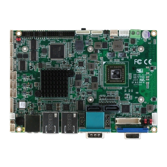
Page 16: Location Of Connectors And Jumpers
S u b C o m p a c t B o a r d G E N E - H D 0 5 2.2 Location of Connectors and Jumpers Component Side Component Side Chapter 2 Quick Installation Guide... - Page 17 S u b C o m p a c t B o a r d G E N E - H D 0 5 Solder Side Solder Side Chapter 2 Quick Installation Guide...
-
Page 18: Mechanical Drawing
S u b C o m p a c t B o a r d G E N E - H D 0 5 2.3 Mechanical Drawing Component Side Component Side Chapter 2 Quick Installation Guide... - Page 19 S u b C o m p a c t B o a r d G E N E - H D 0 5 Solder Side Solder Side Chapter 2 Quick Installation Guide...
-
Page 20: List Of Jumpers
S u b C o m p a c t B o a r d G E N E - H D 0 5 2.4 List of Jumpers The board has a number of jumpers that allow you to configure your system to suit your application. -
Page 21: List Of Connectors
S u b C o m p a c t B o a r d G E N E - H D 0 5 2.5 List of Connectors The board has a number of connectors that allow you to configure your system to suit your application. - Page 22 S u b C o m p a c t B o a r d G E N E - H D 0 5 CN21 +5V Output for SATA HDD CN22 LVDS Inverter / Backlight Connector CN23 LVDS Port CN24 COM Port 1 (D-SUB 9) CN25 Realtek LAN (RJ-45) Port 2...
-
Page 23: Setting Jumpers
S u b C o m p a c t B o a r d G E N E - H D 0 5 2.6 Setting Jumpers You configure your card to match the needs of your application by setting jumpers. A jumper is the simplest kind of electric switch. It consists of two metal pins and a small metal clip (often protected by a plastic cover) that slides over the pins to connect them. -
Page 24: Touch Screen 4/5/8-Wire Selection (Jp1)
S u b C o m p a c t B o a r d G E N E - H D 0 5 2.7 Touch Screen 4/5/8-Wire Selection (JP1) 4/8-wire Mode 5-wire Mode F unction 4/8-wire (Default) 1-2 (open) 5-wire 2.8 AT/ATX Power Supply Mode Selection-1 (JP2) AT Mode... -
Page 25: Clear Cmos Selection (Jp4)
S u b C o m p a c t B o a r d G E N E - H D 0 5 2.10 Clear CMOS Selection (JP4) 1 2 3 1 2 3 Normal (Default) Clear CMOS F unction Normal (Default) Clear CMOS 2.11 LVDS Backlight Lightness Up/down Selection (JP5) -
Page 26: Lvds Backlight Lightness Control Mode Selection (Jp7)
S u b C o m p a c t B o a r d G E N E - H D 0 5 2.13 LVDS Backlight Lightness Control Mode Selection (JP7) 1 2 3 1 2 3 PWM Mode VR Mode F unction VR Mode (Default) -
Page 27: Lpc Port (Cn1)
S u b C o m p a c t B o a r d G E N E - H D 0 5 2.16 LPC Port (CN1) LAD0 LAD1 LAD2 LAD3 +3.3V LFRAME# LRESET# LCLK LDRQ0 LDRQ1 SERIRQ Pin Name Signal Type Signal Level LAD0... -
Page 28: Touch Screen Connector (Cn2)
S u b C o m p a c t B o a r d G E N E - H D 0 5 2.17 Touch Screen Connector (CN2) 8 Wires TOP EXCITE BOTTOM EXCITE LEFT EXCITE RIGHT EXCITE TOP SENSE BOTTOM SENSE LEFT SENSE RIGHT SENSE... - Page 29 S u b C o m p a c t B o a r d G E N E - H D 0 5 4 Wires BOTTOM LEFT RIGHT Pin Name Signal Type Signal Level BOTTOM LEFT RIGHT 5 Wires UL(Y) UR(H) LL(L)
-
Page 30: Cpu Fan Connector (Cn3)
S u b C o m p a c t B o a r d G E N E - H D 0 5 Pin Name Signal Type Signal Level UL(Y) UR(H) LL(L) LR(X) SENSE(S) Note: Touch mode can be set by JP1 2.18 CPU FAN Connector (CN3) FAN_TAC FAN_POWER... -
Page 31: External +5Vsb Input Connector (Cn4)
S u b C o m p a c t B o a r d G E N E - H D 0 5 2.19 External +5VSB Input Connector (CN4) PS_ON# +5VSB Pin Name Signal Type Signal Level PS_ON# +5VSB 2.20 External +12V Input Connector (CN5) +12V GND Pin Name... -
Page 32: Digital Io Port Connector (Cn7)
S u b C o m p a c t B o a r d G E N E - H D 0 5 Pin Name Signal Type Signal Level PWR_BTN- PWR_BTN+ HDD_LED- HDD_LED+ SPEAKER- SPEAKER+ PWR_LED- PWR_LED+ H/W RESET- H/W RESET+ 2.22 Digital IO Port Connector (CN7) Pin Name... -
Page 33: Lpt Port Connector (Cn8)
S u b C o m p a c t B o a r d G E N E - H D 0 5 DIO5 +3.3V DIO6 +3.3V DIO7 +3.3V +3.3V +3.3V 2.23 LPT Port Connector (CN8) STROBE# AFD# ERROR# PRINT# SLIN# ACK#... -
Page 34: Com Port 2 Connector (Cn9)
S u b C o m p a c t B o a r d G E N E - H D 0 5 ACK# BUSY SLCT 2.24 COM Port 2 Connector (CN9) 2-21 Chapter 2 Quick Installation Guide... - Page 35 S u b C o m p a c t B o a r d G E N E - H D 0 5 RS-232 Pin Name Signal Type Signal Level ±9V ±9V ±9V RI/+5V/+12V IN/ PWR +5V/+12V RS-422 Pin Name Signal Type Signal Level RS422_TX-...
-
Page 36: Com Port 3 Connector (Cn10)
S u b C o m p a c t B o a r d G E N E - H D 0 5 RS-485 Pin Name Signal Type Signal Level RS485_D- ±5V RS485_D+ ±5V NC/+5V/+12V +5V/+12V Note: COM2 RS-232/422/485 can be set by BIOS setting. Default is RS-232. -
Page 37: Com Port 4 Connector (Cn11)
S u b C o m p a c t B o a r d G E N E - H D 0 5 ±9V ±9V ±9V 2.26 COM Port 4 Connector (CN11) Pin Name Signal Type Signal Level ±9V ±9V ±9V 2-24... -
Page 38: Usb 2.0 Ports 7 Connector (Cn12)
S u b C o m p a c t B o a r d G E N E - H D 0 5 2.27 USB 2.0 Ports 7 Connector (CN12) Pin Name Signal Type Signal Level +5VSB USB7_D- DIFF USB7_D+ DIFF 2.28 USB 2.0 Ports 8 Connector (CN13) -
Page 39: Usb 2.0 Ports 5 Connector (Cn14)
S u b C o m p a c t B o a r d G E N E - H D 0 5 2.29 USB 2.0 Ports 5 Connector (CN14) Pin Name Signal Type Signal Level +5VSB USB5_D- DIFF USB5_D+ DIFF 2.30 USB 2.0 Ports 6 Connector (CN15) -
Page 40: Usb 2.0 Ports 3 Connector (Cn16)
S u b C o m p a c t B o a r d G E N E - H D 0 5 2.31 USB 2.0 Ports 3 Connector (CN16) Pin Name Signal Type Signal Level +5VSB USB3_D- DIFF USB3_D+ DIFF 2.32 USB 2.0 Ports 4 Connector (CN17) -
Page 41: Audio I/O Port Connector (Cn18)
S u b C o m p a c t B o a r d G E N E - H D 0 5 2.33 Audio I/O Port Connector (CN18) MIC_L MIC_R GND_AUDIO LINE_L_IN LINE_R_IN GND_AUDIO LEFT_OUT GND_AUDIO RIGHT_OUT +5V_AUDIO Pin Name Signal Type Signal Level... -
Page 42: Sata Port2 Connector (Cn20)
S u b C o m p a c t B o a r d G E N E - H D 0 5 Pin Name Signal Type Signal Level SATA_TX+ DIFF SATA_TX- DIFF SATA_RX- DIFF SATA_RX+ DIFF 2.35 SATA Port2 Connector (CN20) Pin 1 Pin 7 Pin Name... -
Page 43: Output For Sata Hdd Connector (Cn21)
S u b C o m p a c t B o a r d G E N E - H D 0 5 2.36 +5V Output for SATA HDD Connector (CN21) Pin Name Signal Type Signal Level 2.37 LVDS Inverter / Backlight Connector (CN22) BLK_PWR BKL_CONTROL BKL_ENABLE... -
Page 44: Lvds Port Connector (Cn23)
S u b C o m p a c t B o a r d G E N E - H D 0 5 2.38 LVDS Port Connector (CN23) PIN 29 PIN 30 PIN 1 PIN 2 Pin Name Signal Type Signal Level BKL_ENABLE BKL_CONTROL... -
Page 45: Com Port 1 (D-Sub 9) Connector (Cn24)
S u b C o m p a c t B o a r d G E N E - H D 0 5 LVDS_DA2+ DIFF LVDS_DA3- DIFF LVDS_DA3+ DIFF DDC_DATA +3.3V DDC_CLK +3.3V LVDS_DB0- DIFF LVDS_DB0+ DIFF LVDS_DB1- DIFF LVDS_DB1+ DIFF LVDS_DB2-... -
Page 46: Realtek Lan (Rj-45) Port2 Connector (Cn25)
S u b C o m p a c t B o a r d G E N E - H D 0 5 Pin Name Signal Type Signal Level ±9V ±9V ±9V 2.40 Realtek LAN (RJ-45) Port2 Connector (CN25) ACT/LINK SPEED Pin Name... -
Page 47: Realtek Lan (Rj-45) Port1 Connector (Cn26)
S u b C o m p a c t B o a r d G E N E - H D 0 5 MDI3+ DIFF MDI3- DIFF 2.41 Realtek LAN (RJ-45) Port1 Connector (CN26) ACT/LINK SPEED Pin Name Signal Type Signal Level MDI0+ DIFF... -
Page 48: Hdmi Port Connector (Cn28)
S u b C o m p a c t B o a r d G E N E - H D 0 5 Pin Name Signal Type Signal Level +5VSB USB1_D- DIFF USB1_D+ DIFF +5VSB USB2_D- DIFF USB2_D+ DIFF 2.43 HDMI Port Connector (CN28) Pin Name Signal Type... -
Page 49: Ps/2 Keyboard/Mouse Combo Port Connector (Cn29)
S u b C o m p a c t B o a r d G E N E - H D 0 5 TMDS_ Data0- DIFF TMDS_Clock+ DIFF TMDS_Clock- DIFF +3.3V +3.3V HPLG_DETECT 2.44 PS/2 Keyboard/Mouse Combo Port Connector (CN29) KB_DATA KB_CLK +5VSB... -
Page 50: Vga Port Connector (Cn30)
S u b C o m p a c t B o a r d G E N E - H D 0 5 2.45 VGA Port Connector (CN30) Pin Name Signal Type Signal Level GREEN BLUE RED_GND_RTN GREEN_GND_RTN BLUE_GND_RTN DDC_DATA HSYNC VSYNC... -
Page 51: Uim Card Module Connector (Cn32)
S u b C o m p a c t B o a r d G E N E - H D 0 5 2.46 UIM Card Module Connector (CN32) Pin Name Signal Type Signal Level UIM_PWR UIM_RST UIM_CLK UIM_VPP UIM_DATA 2.47 DDR3 SODIMM Slot (SO-DIMM1) Standard specification... -
Page 52: Mini-Card Slot (Pciea1)
S u b C o m p a c t B o a r d G E N E - H D 0 5 PC10 PC11 PC12 PC13 +3.3V +3.3V PC14 +3.3V +3.3V PC15 PC16 PC17 2.49 Mini-Card Slot (PCIEA1) Pin Name Signal Type Signal Level... - Page 53 S u b C o m p a c t B o a r d G E N E - H D 0 5 +1.5V +1.5V PCIE_CLK_REQ# UIM_PWR UIM_DATA PCIE_REF_CLK- DIFF UIM_CLK PCIE_REF_CLK+ DIFF UIM_RST UIM_VPP W_DISABLE# +3.3V PCIE_RST# +3.3V PCIE_RX- DIFF +3.3VSB...
- Page 54 S u b C o m p a c t B o a r d G E N E - H D 0 5 SMB_CLK +3.3V PCIE_TX- DIFF SMB_DATA +3.3V PCIE_TX+ DIFF USB_D- DIFF USB_D+ DIFF +3.3VSB +3.3V +3.3VSB +3.3V +1.5V +1.5V +3.3VSB...
- Page 55 S u b C o m p a c t B o a r d G E N E - H D 0 5 Below Table for China RoHS Requirements 产品中有毒有害物质或元素名称及含量 AAEON Main Board/ Daughter Board/ Backplane 有毒有害物质或元素 部件名称 铅...
-
Page 56: Bios Setup
S u b C o m p a c t B o a r d G E N E - H D 0 5 Chapter BIOS Setup Chapter 3 AMI BIOS Setup 3-1... -
Page 57: System Test And Initialization
3. The CMOS memory has lost power and the configuration information has been erased. The GENE-HD05 CMOS memory has an integral lithium battery backup for data retention. However, you will need to replace the complete unit when it finally runs down. -
Page 58: Ami Bios Setup
S u b C o m p a c t B o a r d G E N E - H D 0 5 3.2 AMI BIOS Setup AMI BIOS ROM has a built-in Setup program that allows users to modify the basic system configuration. -
Page 59: Setup Menu
S u b C o m p a c t B o a r d G E N E - H D 0 5 Setup Menu Setup submenu: Main Options summary: (default setting) System Date Day MM:DD:YYYY Change the month, year and century. The ‘Day’ is changed automatically. System Time HH : MM : SS Change the clock of the system. - Page 60 S u b C o m p a c t B o a r d G E N E - H D 0 5 Setup submenu: Advanced Options summary: (default setting) ACPI Settings System ACPI Parameters CPU Configuration CPU Configuration Parameters SATA Configuration SATA Device Options Settings USB Configuration...
-
Page 61: Acpi Settings
S u b C o m p a c t B o a r d G E N E - H D 0 5 ACPI Settings Options summary: (default setting) ACPI Sleep State S3 (Suspend to RAM) Select the highest ACPI sleep state the system will enter when the SUSPEND button is pressed. -
Page 62: Cpu Configuration
S u b C o m p a c t B o a r d G E N E - H D 0 5 CPU Configuration Chapter 3 AMI BIOS Setup 3-7... -
Page 63: Sata Configuration
S u b C o m p a c t B o a r d G E N E - H D 0 5 SATA Configuration Options summary: (default setting) OnChip SATA Channel Disabled Enabled En/Disable Serial ATA OnChip SATA Type ACHI Legacy IDE Configure SATA controller operating as Legacy IDE/AHCI mode. - Page 64 S u b C o m p a c t B o a r d G E N E - H D 0 5 USB Configuration Options summary: (default setting) Legacy USB Support Enabled Disabled Auto Enables Legacy USB Support. AUTO option disables legacy support if no USB devices are connected.
- Page 65 S u b C o m p a c t B o a r d G E N E - H D 0 5 If Auto. USB devices less than 530MB will be emulated as Floppy and remaining as Floppy and remaining as hard drive. Forced FDD option can be used to force a HDD formatted drive to boot as FDD(Ex.
- Page 66 S u b C o m p a c t B o a r d G E N E - H D 0 5 F81866 Super IO Configuration Options summary: (default setting) Serial Port 1/2/3/4 Configuration Set Parameters of Serial Port 1/2/3/4 Parallel Port Configuration Set Parameters of Parallel Port Digital...
- Page 67 S u b C o m p a c t B o a r d G E N E - H D 0 5 ERP Function Disabled Enabled ERP Function En/Disable Chapter 3 AMI BIOS Setup 3-12...
- Page 68 S u b C o m p a c t B o a r d G E N E - H D 0 5 Serial Port 1 Configuration Options summary: (default setting) Serial Port Disabled Enabled En/Disable specified serial port. Change Settings Auto IO=3F8h;...
- Page 69 S u b C o m p a c t B o a r d G E N E - H D 0 5 Serial Port 2 Configuration Options summary: (default setting) Serial Port Disabled Enabled En/Disable specified serial port. Change Settings Auto IO=2F8h;...
- Page 70 S u b C o m p a c t B o a r d G E N E - H D 0 5 Serial Port 3 Configuration Options summary: (default setting) Serial Port Disabled Enabled En/Disable specified serial port. Change Settings Auto IO=3E8h;...
- Page 71 S u b C o m p a c t B o a r d G E N E - H D 0 5 Serial Port 4 Configuration Options summary: (default setting) Serial Port Disabled Enabled En/Disable specified serial port. Change Settings Auto IO=2E8h;...
- Page 72 S u b C o m p a c t B o a r d G E N E - H D 0 5 Parallel Port Configuration Options summary: (default setting) Parallel Port Disabled Enabled En/Disable specified parallel port. Change Settings Auto IO=378h;...
- Page 73 S u b C o m p a c t B o a r d G E N E - H D 0 5 Device Mode STD Printer Mode SPP Mode EPP-1.9 and SPP Mode EPP-1.7 and SPP Mode ECP Mode ECP and EPP 1.9 Mode ECP and EPP 1.7 Mode Change the Printer Port mode...
- Page 74 S u b C o m p a c t B o a r d G E N E - H D 0 5 Digital IO Port Configuration Options summary: (default setting) Port 1 Input Output Set GPIO as Input or Output. Port 2 Input Output...
- Page 75 S u b C o m p a c t B o a r d G E N E - H D 0 5 Port 5 Input Output Set GPIO as Input or Output. Port 6 Input Output Set GPIO as Input or Output. Port 7 Input Output...
- Page 76 S u b C o m p a c t B o a r d G E N E - H D 0 5 F81866 H/W Monitor Chapter 3 AMI BIOS Setup 3-21...
- Page 77 S u b C o m p a c t B o a r d G E N E - H D 0 5 Setup submenu: Chipset Options summary: (default setting) North Bridge South Bridge Parameters South Bridge South Bridge Parameters Chapter 3 AMI BIOS Setup 3-22...
-
Page 78: North Bridge
S u b C o m p a c t B o a r d G E N E - H D 0 5 North Bridge Options summary: (default setting) Graphics Configuration Configure Graphics Settings. Chapter 3 AMI BIOS Setup 3-23... -
Page 79: Graphics Configuration
S u b C o m p a c t B o a r d G E N E - H D 0 5 Graphics Configuration Options summary: (default setting) DP0 Output HDMI Disabled NB PCIE Connect Type (Display device) DP1 Output LVDS Disabled... -
Page 80: South Bridge
S u b C o m p a c t B o a r d G E N E - H D 0 5 South Bridge Options summary: (default setting) Power Mode ATX Type AT Type Select power supply mode. MiniCard &... - Page 81 S u b C o m p a c t B o a r d G E N E - H D 0 5 SB HD Azalia Configuration Options summary: (default setting) HD Audio Azalia Auto Device Disabled Enabled Enable Or Disable HD Audio Azalia Device Chapter 3 AMI BIOS Setup 3-26...
- Page 82 S u b C o m p a c t B o a r d G E N E - H D 0 5 Setup submenu: Boot Options summary: (default setting) Quiet Boot Disabled Enabled En/Disable showing boot logo. Launch RTL8111E PXE Disabled OpROM.
- Page 83 S u b C o m p a c t B o a r d G E N E - H D 0 5 Setup submenu: Security Options summary: (default setting) Administrator Not set Password/ User Password You can install a Supervisor password, and if you install a supervisor password, you can then install a user password.
- Page 84 S u b C o m p a c t B o a r d G E N E - H D 0 5 Setup submenu: Save & Exit Options summary: (default setting) Save Changes and Reset Reset the system after saving the changes Discard Changes and Reset Reset system setup without saving any changes...
-
Page 85: Chapter 4 Driver Installation
S u b C o m p a c t B o a r d G E N E - H D 0 5 Chapter Driver Installation 4 - 1 Chapter 4 Driver Installation... - Page 86 S u b C o m p a c t B o a r d G E N E - H D 0 5 The GENE-HD05 comes with a DVD-ROM that contains all drivers and utilities that meet your needs.
- Page 87 S u b C o m p a c t B o a r d G E N E - H D 0 5 4.1 Installation: Insert the GENE-HD05 DVD-ROM into the DVD-ROM Drive. And install the drivers from Step 1 to Step 6 in order. Step 1 – Install Chipset Driver 1.
- Page 88 S u b C o m p a c t B o a r d G E N E - H D 0 5 Step 4 – Install AHCI Driver Please refer to the Appendix D AHCI Setting Step 5 – Install Touch Driver 1.
-
Page 89: Appendix A Programming The Watchdog Timer
S u b C o m p a c t B o a r d G E N E - H D 0 5 Appendix Programming the Watchdog Timer Appendix A Programming the Watchdog Timer A-1... -
Page 90: Programming
S u b C o m p a c t B o a r d G E N E - H D 0 5 A.1 Programming GENE-HD05 utilizes FINTEK 81866 chipset as its watchdog timer controller. Below are the procedures to complete its configuration and the AAEON initial watchdog timer program is also attached based on which you can develop customized program to fit your application. - Page 91 S u b C o m p a c t B o a r d G E N E - H D 0 5 There are three steps to complete the configuration setup: (1) Enter the MB PnP Mode; (2) Modify the data of configuration registers; (3) Exit the MB PnP Mode.
- Page 92 S u b C o m p a c t B o a r d G E N E - H D 0 5 Watch Dog Timer 1, 2, 3 Control Register (Index=F5h,F6h,FAh Default=00h) Appendix A Programming the Watchdog Timer A-4...
-
Page 93: F81866 Watchdog Timer Initial Program
S u b C o m p a c t B o a r d G E N E - H D 0 5 A.2 F81866 Watchdog Timer Initial Program Main (){ aaeonSuperIOOpen(); aaeonWdtSetCountMode(BOOL bMinute); // Set wdt count mode aaeonWdtSetTimeoutCount(BYTE tTimeout); // Set wdt timer aaeonWdtSetEnable(BOOL bEnable); // Enable wdt aaeonSuperIOClose(); } Void aaeonSuperIOOpen(){ // Config F81866 Entry key ... - Page 94 S u b C o m p a c t B o a r d G E N E - H D 0 5 Void aaeonWdtSetTimeoutCount(BYTE tTimeout){ f81866SetLdn(0x07); f81866WriteByte(F81866_WDT_TIME_REG, tTimeout); } Void aaeonWdtSetEnable(BOOL bEnable){ f81866SetLdn(0x07); if(bEnable){ ...
- Page 95 S u b C o m p a c t B o a r d G E N E - H D 0 5 Void aaeonSuperIOClose(){ aaeonioWritePortByte(F81866_INDEX, 0xaa); } Appendix A Programming the Watchdog Timer A-7...
-
Page 96: Appendix B I/O Information
S u b C o m p a c t B o a r d G E N E - H D 0 5 Appendix I/O Information Appendix B I/O Information... -
Page 97: I/O Address Map
S u b C o m p a c t B o a r d G E N E - H D 0 5 B.1 I/O Address Map Appendix B I/O Information... - Page 98 S u b C o m p a c t B o a r d G E N E - H D 0 5 Appendix B I/O Information...
-
Page 99: St Mb Memory Address Map
S u b C o m p a c t B o a r d G E N E - H D 0 5 B.2 1 MB Memory Address Map Appendix B I/O Information... -
Page 100: Irq Mapping Chart
S u b C o m p a c t B o a r d G E N E - H D 0 5 B.3 IRQ Mapping Chart B.4 DMA Channel Assignments Appendix B I/O Information... - Page 101 S u b C o m p a c t B o a r d G E N E - H D 0 5 Appendix Mating Connector C - 1 Appendix C Mating Connector...
-
Page 102: List Of Mating Connectors And Cables
S u b C o m p a c t B o a r d G E N E - H D 0 5 C.1 List of Mating Connectors and Cables The table notes mating connectors and available cables. Mating Connector Connector Available Function... - Page 103 S u b C o m p a c t B o a r d G E N E - H D 0 5 USB Port Wafer CN15 Molex 51021-0500 1700050207 Connector Cable USB Port Wafer CN16 Molex 51021-0500 1700050207 Connector Cable USB Port...
- Page 104 S u b C o m p a c t B o a r d G E N E - H D 0 5 A ppendix AHCI Setting Appendix D AHCI Setting...
-
Page 105: Setting Ahci
S u b C o m p a c t B o a r d G E N E - H D 0 5 D.1 Setting AHCI OS installation to setup AHCI Mode. Step 1: Copy the files below from “Driver DVD -> STEP4 - AHCI\WinXP\SB8xx_RAID_XP_3.2.1540.92”... - Page 106 S u b C o m p a c t B o a r d G E N E - H D 0 5 Step 3: BIOS Setup menu select “Advanced\OnChip SATA Type -> AHCI” Step 4: Setup OS Appendix D AHCI Setting...
- Page 107 S u b C o m p a c t B o a r d G E N E - H D 0 5 Step 5: Press “F6” Step 6: Choose “S” Appendix D AHCI Setting...
- Page 108 S u b C o m p a c t B o a r d G E N E - H D 0 5 ® Step 7: Choose “AMD A50M” Step 8: It will show the model number you select and then press “ENTER” Step 9: Setup is loading files Appendix D AHCI Setting...
- Page 109 S u b C o m p a c t B o a r d G E N E - H D 0 5 A ppendix AHCI Setting Appendix D AHCI Setting...
- Page 110 S u b C o m p a c t B o a r d G E N E - H D 0 5 D.1 Setting AHCI OS installation to setup AHCI Mode. Step 1: Copy the files below from “Driver DVD -> STEP4 - AHCI\WinXP\SB8xx_RAID_XP_3.2.1540.92”...
- Page 111 S u b C o m p a c t B o a r d G E N E - H D 0 5 Step 3: BIOS Setup menu select “Advanced\OnChip SATA Type -> AHCI” Step 4: Setup OS Appendix D AHCI Setting...
- Page 112 S u b C o m p a c t B o a r d G E N E - H D 0 5 Step 5: Press “F6” Step 6: Choose “S” Appendix D AHCI Setting...
- Page 113 S u b C o m p a c t B o a r d G E N E - H D 0 5 ® Step 7: Choose “AMD A50M” Step 8: It will show the model number you select and then press “ENTER” Step 9: Setup is loading files Appendix D AHCI Setting...
-
Page 114: Electrical Specifications
S u b C o m p a c t B o a r d G E N E - H D 0 5 Appendix Electrical Specifications for I/O Ports Appendix E Electrical Specifications for I/O Ports... -
Page 115: Electrical Specifications For I/O Ports
S u b C o m p a c t B o a r d G E N E - H D 0 5 E.1 Electrical Specifications for I/O Ports Reference Signal Name Rate Output LVDS Inverter / +5V/2A or Backlight CN22 +12V/2A... - Page 116 S u b C o m p a c t B o a r d G E N E - H D 0 5 +3.3VSB +3.3V/1.1A Mini-Card Slot PCIEA1 +1.5V +1.5V/0.375A Appendix E Electrical Specifications for I/O Ports...
Need help?
Do you have a question about the GENE-HD05 and is the answer not in the manual?
Questions and answers