Table of Contents
Advertisement
Quick Links
Download this manual
See also:
User Manual
Advertisement
Table of Contents

Subscribe to Our Youtube Channel
Related Manuals for Measurement Computing PCI-DAS4020/12


Summary of Contents for Measurement Computing PCI-DAS4020/12
- Page 2 PCI-DAS4020/12 Analog & Digital I/O User’s Guide Document Revision 9A, May, 2009 © Copyright 2009, Measurement Computing Corporation...
- Page 3 Other product and company names mentioned herein are trademarks or trade names of their respective companies. © 2009 Measurement Computing Corporation. All rights reserved. No part of this publication may be reproduced, stored in a retrieval system, or transmitted, in any form by any means, electronic, mechanical, by photocopying, recording, or otherwise without the prior written permission of Measurement Computing Corporation.
-
Page 5: Table Of Contents
Overview: PCI-DAS4020/12 features ........................ 8 Software features ..............................8 Chapter 2 Installing the PCI-DAS4020/12 ......................9 What comes with your PCI-DAS4020/12 shipment? ..................9 Hardware ..................................9 Additional documentation ..............................9 Optional components ................................ 9 Unpacking the PCI-DAS4020/12 ........................10 Installing the software ............................ - Page 6 PCI-DAS4020/12 User's Guide Environmental ..............................25 Power consumption ............................26 Connector and pin out ............................26 Auxiliary connector P3 pinout ............................26 Declaration of Conformity ........................27...
-
Page 7: Preface
About this User's Guide What you will learn from this user's guide This user's guide explains how to install, configure, and use the PCI-DAS4020/12 so that you get the most out of its analog and digital I/O features. This user's guide also refers you to related documents available on our web site, and to technical support resources. -
Page 8: Introducing The Pci-Das4020/12
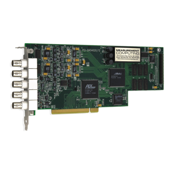
Introducing the PCI-DAS4020/12 Overview: PCI-DAS4020/12 features This manual explains how to install and use the PCI-DAS4020/12 board. The PCI-DAS4020/12 is a multi-function high-speed data acquisition I/O board that is designed for the PCI bus. It provides the following features: ... -
Page 9: Installing The Pci-Das4020/12
In addition to this hardware user's guide, you should also receive the Quick Start Guide (available in PDF at www.mccdaq.com/PDFmanuals/DAQ-Software-Quick-Start.pdf). This booklet supplies a brief description of the software you received with your PCI-DAS4020/12 and information regarding installation of that software. Please read this booklet completely before installing any software or hardware. -
Page 10: Unpacking The Pci-Das4020/12
As with any electronic device, you should take care while handling to avoid damage from static electricity. Before removing the PCI-DAS4020/12 from its packaging, ground yourself using a wrist strap or by simply touching the computer chassis or other grounded object to eliminate any stored static charge. -
Page 11: Connecting The Board For I/O Operations
PCI-DAS4020/12 User's Guide Installing the PCI-DAS4020/12 Connecting the board for I/O operations Connectors, cables – I/O connectors The table below lists the board connectors, applicable cables, and compatible accessory products for the PCI- DAS4020/12. Board connectors, cables, compatible hardware BNC connector: five standard female connectors Connector type ... -
Page 12: Pin Out - Auxiliary Connector
PCI-DAS4020/12 User's Guide Installing the PCI-DAS4020/12 Pin out – auxiliary connector The pin out for the board’s 40-pin on-board auxiliary connector (labeled on the board) is listed below. Pin 1 is identified by a beveled edge on the board silkscreen. - Page 13 Figure 3. C40-37F-x cable If you don’t need to connect to the PCI-DAS4020/12 analog outputs (pins 38 to 40), you can connect to a BP40-37 cable. The BP40-37 cable brings pins 1 through 37 of the 40-pin connector out to 37-pin male "D"...
- Page 14 PCI-DAS4020/12 User's Guide Installing the PCI-DAS4020/12 FIRSTPORTA BIT 0 FIRSTPORTA BIT 1 FIRSTPORTA BIT 2 FIRSTPORTA BIT 3 FIRSTPORTA BIT 4 FIRSTPORTA BIT 5 FIRSTPORTA BIT 6 FIRSTPORTA BIT 7 FIRSTPORTC BIT 0 FIRSTPORTC BIT 1 FIRSTPORTB BIT 1 FIRSTPORTC BIT 2...
- Page 15 PCI-DAS4020/12 User's Guide Installing the PCI-DAS4020/12 40-pin to 37-pin signal mapping Signal mapping on the C40-37F-x and the BP40-37 cables is not 1:1. The following table lists the pin numbers of the signals on the 40-pin end and the pin numbers of the associated signals on the 37-pin end.
-
Page 16: Field Wiring, Signal Termination And Conditioning
Details on these products are available on our web site at www.mccdaq.com/products/screw_terminal_bnc.aspx. Digital Signal Conditioning For digital signal conditioning, you can connect the PCI-DAS4020/12 to the following boards using the C40- 37F-x cable directly or by combining the BP40-37-x cable with the C37FF-x or C37FFS-x cable. -
Page 17: Chapter 3 Functional Details
Chapter 3 Functional Details PCI-DAS4020/12 block diagram PCI-DAS4020/12 functions are illustrated in the block diagram shown here. Four analog input channels per board Attenuator/ Amplifier Four Channels Input VREF CONV 50 Ohm Gain & Offset External Pacer AUTOCAL TRIG1, TRIG2,... -
Page 18: Analog Output
The PCI-DAS4020/12 board is powered by the PCI bus. The only power used is +5 V. Input impedance configuration Each analog input and the trigger/clock input channel on the PCI-DAS4020/12 has a dedicated solder gap. A solder gap consists of two copper pads that you can solder together to change the input impedance of the channel. - Page 19 PCI-DAS4020/12 User's Guide Functional Details Solder Gap Configuration Input Impedance Open 1.5 M typical Close The board designation for the analog input channels and the trigger/clock BNC input are listed below. Solder Gap board label Channel Channel 0 Channel 1...
- Page 20 PCI-DAS4020/12 User's Guide Functional Details An example of each input impedance configuration option is shown in Figure 12. Solder gap SG3 is open (1.5 Mohms) Solder gap SG4 is closed (50 ohms) Figure 12. Open and closed solder gaps...
-
Page 21: Calibrating The Pci-Das4020/12
D/A converters. No external equipment or user adjustments are required. The PCI-DAS4020/12 is factory calibrated. The calibration coefficients are stored in nvRAM. Analog input adjustments are made via 10-bit calibration DACs that are referenced to the on-board factory calibrated standard. -
Page 22: Chapter 5 Specifications
Chapter 5 Specifications Typical for 25 °C unless otherwise specified. Specifications in italic text are guaranteed by design. Analog input Table 1. Analog input specifications A/D converter type AD9225, 25 MSPS pipelined A/D Resolution 12-bits Programmable ranges ±5 V, ±1 V 4 single-ended, independent ADC’s per channel Number of channels Connection... -
Page 23: Accuracy
PCI-DAS4020/12 board is ±7.0 LSB. Each PCI-DAS4020/12 board is tested at the factory to make sure that its actual worst case error is less than ±5.0 LSB. Allowing for a 10% guard-band, the absolute worst-case error of a board is ±5.5 LSB. Typical accuracy can be calculated from the various component typical errors in a similar fashion. -
Page 24: Dynamics And Noise
PCI-DAS4020/12 User's Guide Specifications Dynamics and noise Table 6. Dynamics and noise specifications SNR (Signal-to-noise ratio) 66.6 dB SINAD (signal-to-noise and distortion ratio) 66.5 dB SFDR (spurious free dynamic range) 80 dB THD (total harmonic distortion) 80 dB Noise distribution: (Rate = 10 KHz-20 MHz, Average % ±... -
Page 25: Accuracy
PCI-DAS4020/12 User's Guide Specifications Accuracy Table 9. Analog output accuracy specifications Absolute accuracy ±13 LSB max Offset error ±6 LSB max Gain error ±5 LSB max Differential non-linearity ±1 LSB max Integral non-linearity ±1 LSB max Total analog output error is a combination of gain, offset, integral linearity, and differential linearity error. The overall absolute worst-case error of the board may be calculated by summing these component errors. -
Page 26: Power Consumption
PCI-DAS4020/12 User's Guide Specifications Power consumption Table 13. Power consumption specifications +5 V Operating (A/D to FIFO) 1.5 A typical, 2.0 A max Connector and pin out Table 14. Connector specifications Connector type BNC connector: five standard female connectors Auxiliary connector (P3): 40-pin header connector... -
Page 27: Declaration Of Conformity
Norton, MA 02766 Category: Electrical equipment for measurement, control and laboratory use. Measurement Computing Corporation declares under sole responsibility that the product PCI-DAS4020/12 to which this declaration relates is in conformity with the relevant provisions of the following standards or other documents: EC EMC Directive 2004/108/EC: General Requirements, EN 61326-1:2006 (IEC 61326-1:2005). - Page 28 Measurement Computing Corporation 10 Commerce Way Suite 1008 Norton, Massachusetts 02766 (508) 946-5100 Fax: (508) 946-9500 E-mail: info@mccdaq.com www.mccdaq.com...
Need help?
Do you have a question about the PCI-DAS4020/12 and is the answer not in the manual?
Questions and answers