Sign In
Upload
Manuals
Brands
Renesas Manuals
Recording Equipment
IAR KickStart Kit R-IN32M4-CL3
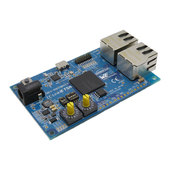
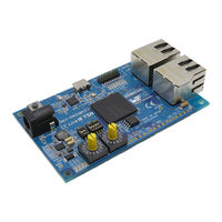
Renesas IAR KickStart Kit R-IN32M4-CL3 Manuals
Manuals and User Guides for Renesas IAR KickStart Kit R-IN32M4-CL3. We have
2
Renesas IAR KickStart Kit R-IN32M4-CL3 manuals available for free PDF download: User Manual, Getting Started Manual
Renesas IAR KickStart Kit R-IN32M4-CL3 User Manual (76 pages)
Brand:
Renesas
| Category:
Computer Hardware
| Size: 1.64 MB
Table of Contents
Table of Contents
6
Overview
12
Definition of Pin Handling and Symbols in this Manual
12
Figure 1.1 Definition of GND Symbols
12
Table 1.1 Definition of Pin Handling
12
Power/Reset Pins
13
Power-On/Off Sequence
13
Table 2.1 External Power Supply
13
Power-On/Off Sequence Without 2.5-V Built-In Regulator
14
Figure 2.1 Power-On/Off Sequence (Without 2.5-V Built-In Regulator)
14
Figure 2.2 Power Supply Channel to R-IN32M4-CL3 (Without 2.5-V Built-In Regulator)
14
Power-On/Off Sequence with 2.5-V Built-In Regulator
15
Figure 2.3 Power-On/Off Sequence (with 2.5-V Built-In Regulator)
15
Figure 2.4 Power Supply Channel to R-IN32M4-CL3 (with 2.5-V Built-In Regulator)
15
Power Supply Pins
16
Reset Pins
17
Clock Input Pins
18
Pin Functions
18
Notes on Configuring the Oscillation Circuit
19
Figure 3.1 Example of GND Pattern for the Components for External Constants
19
Configuration Example of Oscillation Circuits
20
Figure 3.2 Configuration Example of the Oscillation Circuit
20
PLL Power Supply Pins
21
Recommended Configuration of Filter
21
Figure 4.1 Recommended Configuration of Filter
21
Notes on Placement of Peripheral Components
22
Figure 4.2 Schematic View from below the Board
22
GPIO Port Pins
23
Gigabit Ethernet PHY Pins
24
Power Supply Peripheral Circuit
24
Circuit Configuration
24
Figure 6.1 Configuration of Gigabit Ethernet PHY Power Supply Peripheral Circuit
24
Recommended Components
25
Figure 6.2 Example of Recommended Impedance Characteristics with Frequency of Ferrite Beads
25
Table 6.1 Example of Recommended Components of Ceramic Capacitors
25
Table 6.2 Example of Recommended Components of Ferrite Beads
25
Peripheral Circuit of Pulse Transformer
26
Example of Circuit Configuration
26
Figure 6.3 Peripheral Connection Example of Pulse Transformer
26
Recommended Components
27
Figure 6.4 Example of Return Loss of Pulse Transformer
27
REF_REXT and REF_FILT Pins
28
Example of Circuit Configuration
28
Recommended Resistors
28
Recommended Ceramic Capacitors
28
Figure 6.5 Example of Circuit Configuration for REF_REXT and REF_FILT
28
Notes on Board Wiring
29
Figure 6.6 Example of Wiring for Differential Signals (1)
29
Figure 6.7 Example of Wiring for Differential Signals (2)
30
Figure 6.8 Example of Wiring for Differential Signals (3)
30
Unused Gbe-PHY
31
Figure 6.9 Example of Wiring for Differential Signals (4)
31
5-V Built-In Regulator Peripheral Circuit Configuration
32
Peripheral Connection Configuration with 2.5-V Built-In Regulator
32
Peripheral Connection Configuration Without 2.5-V Built-In Regulator
32
Figure 7.1 Peripheral Connection Configuration with 2.5-V Built-In Regulator
32
Figure 7.2 Peripheral Connection Configuration Without 2.5-V Built-In Regulator
32
Recommended Components of Inductor and Capacitors
33
Recommended Component of Schottky Barrier Diode
33
Table 7.1 Example of Recommended Component of Inductor
33
Table 7.2 Capacitance Definition
33
Table 7.3 Example of Recommended Components of Ceramic Capacitors
33
Table 7.4 Example of Recommended Components of Schottky Barrier Diode
33
Example of PCB Layout Image (23 MM Square BGA Package)
34
L1 and L2 (23 MM Square BGA Package)
34
L3 and L4 (23 MM Square BGA Package)
34
Figure 7.3 Example of PCB Layout Image (L1 and L2) (23 MM Square BGA Package)
34
Figure 7.4 Example of PCB Layout Image (L3 and L4) (23 MM Square BGA Package)
34
Example of PCB Layout Image (17 MM Square BGA Package)
35
L1 and L2 (17 MM Square BGA Package)
35
L3 and L4 (17 MM Square BGA Package)
35
Figure 7.5 Example of PCB Layout Image (L1 and L2) (17 MM Square BGA Package)
35
Figure 7.6 Example of PCB Layout Image (L3 and L4) (17 MM Square BGA Package)
35
In out
35
Requirements for Parasitic Resistances and Parasitic Inductances in PCB
36
Table 7.5 Requirements for Parasitic Resistances and Parasitic Inductances in PCB
36
Thermal Design
37
Deciding on Whether Particular Measures for Heat Dissipation Are Required
37
Estimating Tj
37
Estimating Power Consumption
37
Thermal Resistances under the JEDEC Conditions (for Θja and Ψjt)
37
Examples of Measures for Heat Dissipation
38
Measures for Heat Release in Designing the Board
39
Heat Dissipation from the Periphery (Including the Casing)
41
Caution
42
Handling of Unused Pins
42
External Mcu/Memory Interface Pins
43
Table 9.1 Mode Selection of External Mcu/Memory Connection
43
External MCU Interface
44
Asynchronous-SRAM Supporting MCU Connection Mode
45
Figure 9.1 Connection Example of 32-Bit External MCU Interface
45
Figure 9.2 Connection Example of 16-Bit External MCU Interface
45
Synchronous-SRAM Supporting MCU Connection Mode
46
Synchronous-Burst-Transfer Supporting MCU Connection Mode
47
Figure 9.5 Connection Example of 32-Bit External MCU Interface
47
Figure 9.6 Connection Example of 16-Bit External MCU Interface
47
Figure 9.7 Connection Example of 32-Bit External MCU Interface
49
Figure 9.8 Connection Example of 16-Bit External MCU Interface
49
External Memory Interface
50
Asynchronous SRAM MEMC
50
Figure 9.9 Connection Example with 32-Bit SRAM (Asynchronous SRAM MEMC)
51
Figure 9.10 Connection Example with 16-Bit SRAM (Asynchronous SRAM MEMC)
51
Figure 9.11 Connection Example with 32-Bit Paged ROM (Asynchronous SRAM MEMC)
52
Figure 9.12 Connection Example with 16-Bit Paged ROM (Asynchronous SRAM MEMC)
52
Synchronous Burst Access MEMC
53
Figure 9.13 Connection Example with 32-Bit SRAM (Synchronous Burst Access MEMC)
54
Figure 9.14 Connection Example with 16-Bit SRAM (Synchronous Burst Access MEMC)
54
Figure 9.15 Connection Example with 32-Bit Paged ROM (Synchronous Burst Access MEMC)
55
Figure 9.16 Connection Example with 16-Bit Paged ROM (Synchronous Burst Access MEMC)
55
Serial Flash ROM Connection Pins
56
Figure 10.1 Connection Example with Serial Flash ROM
56
Asynchronous Serial Interface J Connection Pins
57
Figure 11.1 Connection Example between R-IN32M4-CL3 and UART Device
57
I 2 C Connection Pins
58
Figure 12.1 Connection Example between R-IN32M4-CL3 and I
58
CAN Pins
59
Figure 13.1 Connection Example between R-IN32M4-CL3 and CAN Transceiver
59
CSIH Pins
60
One Master and One Slave
60
One Master and Two Slaves
60
Figure 14.1 Direct Master/Slave Connection
60
Figure 14.2 Connection between One Master and Two Slaves
60
Jtag/Trace Pins
61
Figure 15.1 Connection Example of JTAG Interface (20-Pin Half-Pitch Without Trace)
61
Figure 15.2 Connection Example of JTAG Interface (20-Pin Half-Pitch with Trace)
62
Figure 15.3 Connection Example of SWD Interface (20-Pin Half-Pitch Without Trace)
63
Figure 15.4 Connection Example of JTAG Interface (20-Pin Full-Pitch)
64
Implementation Conditions
65
Figure 16.1 Implementation Flow
65
Figure 16.2 Infrared Reflow Temperature Profile
65
Package Information
66
Figure 17.1 Package Information (23 MM Square BGA Package)
66
Figure 17.2 Package Information (17 MM Square BGA Package)
67
Mount Pad Information
68
Figure 18.1 Mount Pad Sizes (23 MM Square BGA Package)
68
Figure 18.2 Mount Pad Sizes (17 MM Square BGA Package)
68
BSCAN Information
69
BSCAN Operating Conditions
69
Maximum Operating Frequency of TCK
69
Idcode
69
BSCAN Non-Supported Pins
69
How to Get BSDL
69
Table 19.1 List of BSCAN Non-Supported Pins
69
IBIS Information
70
Marking Information
71
Figure 21.1 R-IN32M4-CL3 Marking Information (23 MM Square BGA Package)
71
Figure 21.2 R-IN32M4-CL3 Marking Information (17 MM Square BGA Package)
71
Countermeasure for Noise
72
Stopping Clock Output
72
Advertisement
Renesas IAR KickStart Kit R-IN32M4-CL3 Getting Started Manual (7 pages)
Brand:
Renesas
| Category:
Recording Equipment
| Size: 1.61 MB
Advertisement
Related Products
Renesas R-IN32M4-CL2 TESSERA
Renesas R-IN32 Series
Renesas R-IN32M3-EC
Renesas R-IN32M3-CL
Renesas R-IN32M3 Series
Renesas RX62N Group
Renesas RTKA223181DE0010BU
Renesas RA2E2 Group
Renesas RS-485
Renesas R5F51103ADFK
Renesas Categories
Computer Hardware
Motherboard
Microcontrollers
Adapter
Switch
More Renesas Manuals
Login
Sign In
OR
Sign in with Facebook
Sign in with Google
Upload manual
Upload from disk
Upload from URL