
Related Manuals for SOLTEK SL-75DRV2


Summary of Contents for SOLTEK SL-75DRV2
- Page 1 T h e S o u l C o m p u t e r T e c h n o l o g y SL-75DRV2 USER MANUAL v1.0...
- Page 2 Soltek Computer Inc. has been advised of the possibility of such damages arising from any defect or error in this manual or product.
-
Page 3: Soltek Computer Inc
SOLTEK AROUND THE WORLD SOLTEK COMPUTER INC. Address : 7F, No. 306-3, Ta-Tung Rd, Sec.1, Hsi-Chih, Taipei- Hsien, Taiwan, R.O.C. Telephone : 886-2-2642-9060 : 886-2-2642-9065 E-mail : sales@soltek.com.tw Web site : http://www.soltek.com.tw SOUL TECHNOLOGY EUROPE B.V. Address : Hongkongstraat 55, 3047 BP Rotterdam. The Neth-... -
Page 4: Table Of Contents
75DRV2/ CONTENT CHAPTER 1 INTRODUCTION ..........8 1-1 MAINBOARD SPECIFICATION ..........9 1-1.1 PROCESSOR ................... 9 1-1.2 CHIPSET ................... 9 1-1.3 AWARD BIOS V6.0 SUPPORTING ........... 9 1-1.4 SOUND CONTROLLER ..............9 1-1.5 POWER MANAGEMENT ..............9 1-1.6 FULL FEATURED ACCELERATED GRAPHICS PORTS (AGP) CONTROLLER ................ - Page 5 Content 2-5.3 Frequency Ratio Select (By SW1 DIP1-DIP5) ........ 24 2-5.4 Processor Core Voltage Select (By SW2 DIP1-DIP6) ..... 25 2-5.5 CPU External Frequency Setting (By SW3) ........26 2-6 JUMPER SETTING FOR DEVICES ON BOARD ....27 2-6.1 JP1/JP2 Memory Module Voltage Select ........27 2-6.2 JP17 Power Lost Resume ...............
- Page 6 75DRV2/ CHAPTER 4 BIOS SETUP ........... 48 4-1 WHAT IS BIOS SETUP ............49 4-2 HOW TO RUN BIOS SETUP ........... 49 4-3 WHAT IS CMOS ..............49 4-4 WHAT IS POST ............... 49 4-5 BIOS UPGRADE ..............49 4-5.1 BEFORE UPGRADING BIOS ............50 4-5.2 UPGRADE PROCESS ..............
-
Page 7: Item List Checkup
Content ITEM LIST CHECKUP Mainboard ==== Support CD ==== User’s Manual ==== Bundled Bonus Pack CD ==== Bundled Bonus Pack Manual ==== Temperature Sensor Cable ==== ATA66/100 IDE Cable ==== RS232 Cable FDD Cable... -
Page 8: Chapter 1 Introduction
75DRV2 CHAPTER INTRODUCTION • This chapter briefly introduces the characteristics of the mainboards. It includes the information regarding the chipset, CPU types, built-in functions and layout. Users will have more ideas about mainboards after reading this chapter. This chapter contains the following topics : 1-1 MAINBOARD SPECIFICATION 1-2 MAINBOARD LAYOUT 1-3 CHIPSET DIAGRAM... -
Page 9: Mainboard Specification
Chapter 1 Introduction 1-1 MAINBOARD SPECIFICATION 1-1.1 PROCESSOR • Supporting Socket A-based AMD Athlon™/Duron™/Athlon 4™ processors. • Supporting 200MHz & 266MHz FSB bus. • Supporting Processor VID(voltage ID) and FID(Frequency ID) auto detection. 1-1.2 CHIPSET • North Bridge: VIA VT8366A KT-266A. •... -
Page 10: 1-1.6 Full Featured Accelerated Graphics Ports (Agp)
75DRV2 1-1.6 FULL FEATURED ACCELERATED GRAPHICS PORTS (AGP) CONTROLLER • AGP v2.0 compliant. • Supports Side Band Addressing(SBA) mode (non-multiplexed address / data). • Supporting 66MHz 1x, 2x, and 4x modes for AD and SBA signaling. 1-1.7 MULTI-I/O FUNCTION • Two UltraDMA-33/66/100 Master Mode PCI EIDE ports. •... -
Page 11: 1-1.10 Form Factor
Chapter 1 Introduction 1-1.10 FORM FACTOR • ATX form factor, 4- layer PCB. • Mainboard size 22.0cm x 30.5cm. 1-1.11 HARDWARE MONITOR • Programmable control, status to provide, monitoring and alarm for flexible desktop management (software include). • 5 positive voltage statuses monitoring. •... -
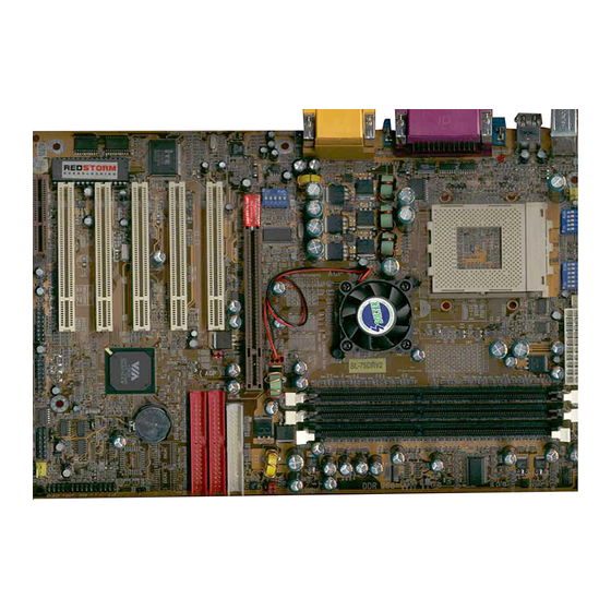
Page 12: Mainboard Layout
75DRV2 1-2 MAINBOARD LAYOUT 5 4 3 2 1 6 5 4 3 2 1 FAN2 FAN1 SOCKET A SSF1 VT8366A AGP PRO 4X FDC1 AC'97 Codec PCI 1 IDE1 PCI 2 IDE2 JCD_IN1 LPC I/O Controller PCI 3 Battery VT8233 PCI 4 WOL1... -
Page 13: Chipset Diagram
Chapter 1 Introduction 1-3 CHIPSET DIAGRAM • The VT8366A and VT8233 chipset is a high performance, cost-effective and energy efficient system controller for the implementation of AGP / PCI / ISA desktop personal computer system based on 64-bit Socket-A (AMD Athlon) processors. SYSCLK, SYSCLK# Athlon INTR, NMI, SM#, STPCLK#,... - Page 14 75DRV2 MEMO MEMO...
-
Page 15: Chapter 2 Hardware Setup
Chapter 2 Hardware Setup CHAPTER HARDWARE SETUP ATTENTION !!! 1. Please refer to your processor installation or other documentation attached to your CPU for detailed in- stalling instruction. 2. Installing a heat sink and cooling fan is necessary for proper heat dissipation from your CPU. Incorrect installation may result in overheating and damage of your CPU. -
Page 16: Cpu Installation
75DRV2 2-1 CPU INSTALLATION WARNING !!! • Make sure that +5V DCV and +3.3 DCV capabilities of your power supply are suitable for the processor. • Any attempt to operate the AMD Athlon or Duron processor without a suitable cooling Fan will damage processor and other component. Pull out the lever from the socket, and then raise the lever up to a 90-degree angle. -
Page 17: Memory Installation
Chapter 2 Hardware Setup 2-2 MEMORY INSTALLATION WARNING!!! • Make sure to unplug your power supply before adding or removing memory modules or other system components. Failure to do so may cause severe damage to both your mainboard and expansion cards. •... - Page 18 75DRV2 5 4 3 2 1 6 5 4 3 2 1 FAN2 FAN1 SOCKET A SSF1 VT8366A AGP PRO 4X N O T I C E : W h e n L E D FDC1 AC'97 “ZD1” is on, meaning that Codec PCI 1 IDE1...
-
Page 19: Accelerated Graphics Port(Agp) Pro Installation
Chapter 2 Hardware Setup 2-3 ACCELERATED GRAPHICS PORT(AGP) PRO INSTALLATION • The AGP Pro connector is an extension of the existing AGP connector and it is compatible with existing AGP cards. AGP Accelerator AGP Pro slot blockader Accelerated Graphics Port (AGP) Pro Slot Rib(inside slot) 20-pin bay Rib(inside slot) 28-pin bay... -
Page 20: Hdd/Fdd Installation
75DRV2 2-4 HDD/FDD INSTALLATION • To install HDD (Hard Disk Drive), you may connect the cable’s blue connector to the mainboard’s primary (IDE1) or secondary (IDE2) connector, and then connect the gray connector to your slave device and the black connector to your master device. If you install two hard disks, you must configure the second drive to Slave mode by setting its jumper accordingly. - Page 21 Chapter 2 Hardware Setup • To install FDD (Floppy Disk Drive), you may connect the single end to the board , and connect two plugs on the other end to the floppy drives. 6 5 4 3 2 1 5 4 3 2 1 FAN2 FAN1 SOCKET A...
-
Page 22: Switch Setting For Cpu Frequency And Voltage
75DRV2 2-5 SWITCH SETTING FOR CPU FREQUENCY AND VOLTAGE 2-5.1 Information On AMD Socket 462 Processor (Model 4, 5 Products) • On the AMD Socket 462 Processor, you can find a codified identification marking which is to provide useful information about the CPU. The marking is interpreted as below. -
Page 23: 2-5.2 Information On Amd Socket 462 Processor (Model 6, 7 Products)
Chapter 2 Hardware Setup 2-5.2 Information On AMD Socket 462 Processor (Model 6, 7 Products) XXXXXXXXXXX XXXXXXXXXXXX XXXXXXX XXXXXXXXX XXXXXXXXXXX XXXX AMD XXXX A HD 1533 HD 1533 A N S 3 C N S 3 C 4 5 6 7 8 Family/Architecture: A= AMD Athlon™Model 6 Processor Architure. -
Page 24: 2-5.3 Frequency Ratio Select (By Sw1 Dip1-Dip5)
75DRV2 2-5.3 Frequency Ratio Select (By SW1 DIP1-DIP5) • The AMD Athlon and Duron processors provides four Frequency ID signals (FID) for the system controller to indicate the SYSTCLK multiplier at which the processor core operates. Normally, multiplier (or bus ratio) is detected automatically. -
Page 25: 2-5.4 Processor Core Voltage Select (By Sw2 Dip1-Dip6)
Chapter 2 Hardware Setup 2-5.4 Processor Core Voltage Select (By SW2 DIP1-DIP6) • DIP1-DIP6 SW2 allow you to adjust processor core voltage manually. We recommend to leave SW2 DIP1 at default, the default means the correct processor core voltage is generated according to VID of CPU. SW2 DIP2 ~ DIP6 SETTING SW2 DIP1 6 5 4 3 2 1... -
Page 26: 2-5.5 Cpu External Frequency Setting (By Sw3)
75DRV2 2-5.5 CPU External Frequency Setting (By SW3) CPU EXTERNAL CLOCK PCI CLOCK FSB CLOCK 100MHz 33.3MHz 200MHz (Default) 120MHz 30.0MHz 240MHz 133.3MHz 33.3MHz 266MHz 140MHz 35.0MHz 280MHz 150MHz 37.5MHz 300MHz IMPORTANT: • Do figure out the correct processor type by processor’s OPN (Ordering Part Numbers). -
Page 27: Jumper Setting For Devices On Board
Chapter 2 Hardware Setup 2-6 JUMPER SETTING FOR DEVICES ON BOARD • The following diagrams show the location for jumper blocks on the mainboard. CAUTION !! • Do not remove the jumper when power is on. Always make sure the power is off before changing any jumpers. -
Page 28: 2-6.2 Jp17 Power Lost Resume
75DRV2 2-6.2 JP17 Power Lost Resume 5 4 3 2 1 6 5 4 3 2 1 FAN2 FAN1 SOCKET A SSF1 VT8366A Power Lost Resume: AGP PRO 4X FDC1 AC'97 Normal Codec PCI 1 JP17 IDE1 (default) PCI 2 IDE2 JCD_IN1 LPC I/O... -
Page 29: 2-6.4 Jbat1 For Clear Cmos Data
Chapter 2 Hardware Setup 2-6.4 JBAT1 For Clear CMOS Data A battery must be used to retain the mainboard configuration in CMOS RAM. 5 4 3 2 1 6 5 4 3 2 1 FAN2 FAN1 SOCKET A SSF1 VT8366A JBAT1 For Clear CMOS Data: AGP PRO 4X FDC1... -
Page 30: Connectors Configurations
75DRV2 2-7 CONNECTORS CONFIGURATIONS • This section lists out all connectors configurations for users’ reference. 2-7.1 On Board FAN Connector (FAN1, FAN2, FAN3, FAN4) On Board FAN Connector (FAN 1: 5 4 3 2 1 6 5 4 3 2 1 FAN2 FAN1 On Board FAN Connector... -
Page 31: 2-7.2 Wol1 Wake On Lan
Chapter 2 Hardware Setup 2-7.2 WOL1 Wake On LAN 5 4 3 2 1 6 5 4 3 2 1 FAN2 FAN1 SOCKET A SSF1 +5V standby VT8366A Wake On LAN: AGP PRO 4X FDC1 AC'97 Codec PCI 1 IDE1 Connect the Wake PCI 2 IDE2... -
Page 32: 2-7.4 Thermal Sensor Connector (Rt2)
75DRV2 2-7.4 Thermal Sensor Connector (RT2) 5 4 3 2 1 6 5 4 3 2 1 FAN2 FAN1 SOCKET A Thermal Sensor Connector (RT2): SSF1 VT8366A AGP PRO 4X FDC1 AC'97 Codec PCI 1 IDE1 PCI 2 IDE2 JCD_IN1 LPC I/O Controller PCI 3... -
Page 33: 2-7.5 Complex Header Con1
Chapter 2 Hardware Setup 2-7.5 Complex Header CON1 • This complex Header consists of 9 connectors providing various supports: CON1 15 15 SUSPEND LED SMI SIGNAL SUSPEND LED SIGNAL POWER SWITCH ATX POWER SWITCH NO CONNECTION NO CONNECTION NO CONNECTION POWER LED NO CONNECTION NO CONNECTION... -
Page 34: 2-7.6 Atx Power Supply Connector
75DRV2 6. Power LED Connector: CONNECTION: Connected to System Power LED. FUNCTION : To supply power to “System Power LED”. 7. Reset Switch Connector: CONNECTION: Connected to the case-mounted “Reset Switch”. FUNCTION : To supply power to “Reset Switch” and support system reboot function. -
Page 35: 2-7.7 Chassis Panel Connector
Chapter 2 Hardware Setup 2-7.7 Chassis Panel Connector A : PS/2 MOUSE PORT B : USB 0 PORT C : LPT1 PORT D : GAME/MIDI PORT E : PS/2 KEYBOARD PORT F : USB 1 PORT G : COM 1 PORT H : COM 2 PORT : LINE OUT / SPEAKER OUT PORT J : LINE IN... -
Page 36: 2-7.8 Smart Card Reader Connector (Scr1)
75DRV2 2-7.8 Smart Card Reader Connector (SCR1) • The connector “SCR1” allows you to use Smart Card Reader. It is compliant with Personal Computer Smart Card (PC/SC) working group standard and smart card (ISO 7816) protocols. 5 4 3 2 1 6 5 4 3 2 1 FAN2 FAN1... -
Page 37: 2-7.9 Communication And Networking Riser Slot (Cnr)
Chapter 2 Hardware Setup 2-7.9 Communication And Networking Riser Slot (CNR) • This connector allows you to use network, modem or audio riser cards. 5 4 3 2 1 6 5 4 3 2 1 FAN2 FAN1 SOCKET A SSF1 VT8366A AGP PRO 4X FDC1... -
Page 38: 2-7.10 Usb Header (Usb2/Usb3 Header)
75DRV2 2-7.10 USB Header (USB2/USB3 Header) • This header is for connecting the additional USB cable to provides you additional two USB ports. User can order the additional USB cable from your mainboard dealer and vender. Additional USB Cable (Optional) red wire Black Black... - Page 39 Chapter 2 Hardware Setup MEMO MEMO...
-
Page 40: Chapter 3 Software Setup
75DRV2 CHAPTER SOFTWARE SETUP Drivers, Utilities and Software Installation • Support CD: This series of mainboards will always be shipped with a Support CD which contains those necessary driver files, Application Softwares and some helpful utilities. It is a user-friendly, auto-run CD which will open itself up in a CD-ROM automatically. -
Page 41: Open Up The Suport Cd And Choose Drivers And Utilities
Chapter 3 Software Setup 3-1 Open up the Suport CD and choose Drivers and Utilities Please put the Support CD enclosed in your mainboard package into the CD-ROM drive. In a few seconds, the Main Menu will automati- cally appear, displaying the contents to be installed for this series: Install VIA 4in1 Driver Install VIA AC’97 Audio Driver Install Hardware Monitor Utility... -
Page 42: Proceed To Via 4-In-1 Drivers Installation
75DRV2 3-2 Proceed to VIA 4-IN-1 Drivers Installation Following the procedures of opening the Support CD, click to “ VIA 4in1 Drivers” to proceed. T h e V I A S e r v i c e P a c k “VIA Service Pack README”... - Page 43 Chapter 3 Software Setup Select “Install VIA ATAPI Vendor Click on “Click to enable DMA Support Driver” checkbox, Mode” checkbox to enable DMA then click the “Next” button to function, then click the “Next” continue. button to continue. Next Next Select “Install VIA AGP VxD”...
-
Page 44: Proceed To Ac'97 Audio Driver Installation
75DRV2 3-3 Proceed to AC’97 AUDIO DRIVER Installation Following the installation of VIA 4in1 drivers, you have to restart system so that your system can be reconfigured with VIA 4in1. When restarting procedures finish, please open the Support CD with your CD-ROM to enter the Main Installation Menu. -
Page 45: Proceed To Hardware Monitor Installation
Chapter 3 Software Setup 3-4 Proceed to HARDWARE MONITOR Installation Following the installation of AC’97 driver, you have to install Hardware Monitor manually. Please click to the following path to execute Hardware Monitor installation: D: \ Hardwaremonitor\ ITE8705 \ Install.exe (assuming that your CD-ROM Drive is Drive D) In case you are already on the Installation Main Menu of the Support CD, please click to the “Install Hardware Monitor”. - Page 46 75DRV2 To display the Hardware Monitor Utility, just click on the “ITE SMARTGUARDIAM” icon in your program file, and the following screen of Smartguardian Control Panel will show up, displaying the information about system temperatures, voltages and Fan speed. Clicking to the “Option”...
- Page 47 Chapter 3 Software Setup MEMO MEMO...
-
Page 48: Chapter 4 Bios Setup
75DRV2 CHAPTER BIOS SETUP THE BIOS • BIOS stands for Basic Input and Output System. It is sometimes called ROM BIOS because it is stored in a Read-Only Memory(ROM) chip on the mainboard. BIOS is the first program to run when you turn on your computer. -
Page 49: What Is Bios Setup
Chapter 4 BIOS Setup 4-1 WHAT IS BIOS SETUP • BIOS setup is an interactive BIOS program that you need to run when: 1. Changing the hardware of your system. (For example: installing a new Hard Disk etc.) 2. Modifying the behavior of your computer. (For example: changing the system time or date, or turning special features on or off etc.) 3. -
Page 50: 4-5.1 Before Upgrading Bios
75DRV2 • The upgrade utility can be loaded on a floppy diskette and used to provides the capability to save, verify, and update the system BIOS. The upgrade utility can be run from a hard disk drive or a network drive. 4-5.1 BEFORE UPGRADING BIOS •... - Page 51 Chapter 4 BIOS Setup Step 4. Type awdflash *.bin /sn/py/cc and then press <Enter> to run BIOS upgrade program. (*.bin depends on your mainboard model and version code. Instead of typing “*”, you should type specific file name for your specific mainboard). Step 5.
- Page 52 75DRV2 Award Flash Memory Writer Start Screen Award Flash Memory Writer Complete Screen...
- Page 53 Chapter 4 BIOS Setup The parameters of AWDFLASH.EXE /sn: No original BIOS backup /py: Program flash memory /cc: Clear CMOS data (and update data automatically) after pro- gramming NOTE: Users can type AWDFLASH /? to get further details about the parameters.
-
Page 54: Bios Setup
75DRV2 4-6 BIOS SETUP --- CMOS SETUP UTILITY 4-6.1 CMOS SETUP UTILITY • This mainboard comes with the AWARD BIOS from AWARD Software Inc. Enter the CMOS Setup Utility Main Menu by: 1. Turn on or reboot your system. After a series of diagnostic checks, the following message will appear: PRESS <DEL>... -
Page 55: 4-6.2 Standard Cmos Setup
Chapter 4 BIOS Setup 4-6.2 STANDARD CMOS SETUP • Standard CMOS Setup records some basic system hardware configuration and sets the system clock and error handling. You only need to modify the configuration values of this option if you want to change your system hardware configuration or when the data stored in the CMOS memory gets lost or damaged. - Page 56 75DRV2 Date (mm:dd:yy) The BIOS determines the day of the week from the other date information. This field is for information only. Press the left or right arrow key to move to the desired field (date, month, year). Press the PgUp or PgDn key to increment the setting, or type the desired value into the field.
- Page 57 Chapter 4 BIOS Setup Drive A / Drive B Select this field to the type(s) of floppy disk drive(s) installed in your system. The choices are: 360KB, 5.25in; 1.2MB, 5.25in; 720KB, 3.5in; 1.44MB, 3.5in; 2.88MB, 3.5in; None. Video Select the type of primary video subsystem in your computer.
-
Page 58: 4-6.3 Advanced Bios Features
75DRV2 4-6.3 ADVANCED BIOS FEATURES • ADVANCED BIOS FEATURES improves your system performance or sets up system features according to your preference. Run the ADVANCED BIOS FEATURES as follows: 1. Choose “ADVANCED BIOS FEATURES” from the Main Menu and a screen with a list of options will appear: CMOS Setup Utility - Copyright (C) 1984-2001 Award Software Advanced BIOS Features... - Page 59 Chapter 4 BIOS Setup 2. Use one of the arrow keys to move between options and modify the selected options by using PgUp / PgDn / + / - keys. An explanation of the <F> keys follows: <F1>: “Help” gives options available for each item. <F5>: Get the previous values.
- Page 60 75DRV2 Quick Power On Self Select Enabled to reduce the amount of time required to Test run the power-on self-test (POST). A quick POST skips certain steps. We recommend that you normally enable quick POST. First/Second/Third/ The BIOS attempts to load the operating system from Other Boot Device the devices in the sequence selected in these items.
- Page 61 Chapter 4 BIOS Setup Typematic Rate Setting When Disabled, the following two items (Typematic Rate and Typematic Delay) are irrelevant. Keystroke repeats at a rate determined by the keyboard controller in your system. When Enabled, you can select a typematic rate and typematic delay.
-
Page 62: 4-6.4 Advanced Chipset Features
75DRV2 4-6.4 ADVANCED CHIPSET FEATURES • ADVANCED CHIPSET FEATURES is used to modify the values of chipset buffers. These buffers control the system options. Run the ADVANCED CHIPSET FEATURES as follows: 1. Choose “ADVANCED CHIPSET FEATURES” from the Main Menu and a list of option will appear: 2. - Page 63 Chapter 4 BIOS Setup DRAM CLOCK/DRIVE CONTROL CMOS Setup Utility - Copyright (C) 1984-2001 Award Software DRAM Clock/Drive Control Item Help Current FSB Frequency 100MHz Menu Level 100MHz DRAM Clock DRAM Timing By SPD SDRAM Cycle Length Bank Interleave Disabled DRAM Command Rate 1T Command :Move Enter:Select +/-/PU/PD:Value F10:Save ESC:Exit F1:General Help...
- Page 64 75DRV2 * DRAM Command The choices: Disabled; 2 Bank; 4 Bank. Rate AGP & P2P BRIDGE CONTROL CMOS Setup Utility - Copyright (C) 1984-2001 Award Software AGP & P2P Bridge Control Item Help AGP Aperture Size Menu Level AGP Mode Auto AGP Driving Control AGP Driving Value...
- Page 65 Chapter 4 BIOS Setup * AGP Driving Value This item allows you to adjust the AGP driving force. The choice: Min=0000 ~ Max=00FF. * AGP Fast Write This item will enable the AGP model into fast write mode. If your graphics card does not support this function, please do not enable this function.
- Page 66 75DRV2 * PCI1 Post Write Leave this field at default. * PCI2 Post Write Leave this field at default. * PCI Delay Transac- Leave this field at default. tion Memory Hole In order to improve performance, certain space in memory is reserved for ISA cards. This memory must be mapped into the memory space below 16MB.
-
Page 67: 4-6.5 Integrated Peripherals
Chapter 4 BIOS Setup 4-6.5 INTEGRATED PERIPHERALS • INTEGRATED PERIPHERALS option allows you to get some information inside your system when it is working. Run the INTEGRATED PERIPHERALS as follows: 1. Choose “INTEGRATED PERIPHERALS” from the Main Menu and a list of options will appear: CMOS Setup Utility - Copyright (C) 1984-2001 Award Software Integrated Peripherals... -
Page 68: Via Onchip Ide Device
75DRV2 VIA ONCHIP IDE DEVICE CMOS Setup Utility - Copyright (C) 1984-2001 Award Software VIA OnChip IDE Device Item Help OnChip IDE Channel0 Enabled OnChip IDE Channel1 Enabled Menu Level IDE Prefetch Mode Enabled Primary Master PIO Auto Primary Slave PIO Auto Secondary Master PIO Auto... -
Page 69: Via Onchip Pci Device
Chapter 4 BIOS Setup * Primary Ultra DMA33/66/100 implementation is possible only Master / Slave UDMA if your IDE hard drive supports it, if the operating Secondary environment includes a DMA drive, and if your Master / Slave UDMA system software both support Ultra DMA33/66/100. Select “Auto”... - Page 70 75DRV2 VIA SUPERIO DEVICE CMOS Setup Utility - Copyright (C) 1984-2001 Award Software VIA SuperIO Device Item Help Onboard FDC Controller Enabled Onboard Serial Port 1 3F8/IRQ4 Menu Level Onboard Serial Port 2 2F8/IRQ3 UART Mode Select Normal UR2 Duplex Mode Half Onboard Parallel Port 378/IRQ7...
- Page 71 Chapter 4 BIOS Setup * UR2 Duplex Mode This item allows you to select the IR half / full duplex function. The choices: Half; Full. * Onboard Parallel Port This item allows you to determine onboard parallel port controller I/O address setting. The choices: 378H/IRQ7;...
- Page 72 75DRV2 USB Keyboard Sup- Select Enabled if your system contains a Universal port Serial Bus (USB) controller and you have a USB keyboard. IDE HDD Block Mode Block mode is also called block transfer, multiple commands, or multiple sector read/write. If your IDE hard drive supports block mode (most new drives do), select Enabled for automatic detection of the optimal number of block read/write per sector the...
-
Page 73: 4-6.6 Power Management Setup
Chapter 4 BIOS Setup 4-6.6 POWER MANAGEMENT SETUP • POWER MANAGEMENT SETUP allows you to set the system’s power saving functions. Run the POWER MANAGEMENT SETUP as follows: 1. Choose “POWER MANAGEMENT SETUP” from the Main Menu and a list of options will appear: CMOS Setup Utility - Copyright (C) 1984-2001 Award Software Power Management Setup Item Help... - Page 74 75DRV2 ACPI Function Select Enabled only if your computer’s operating system supports the Advanced Configuration and Power Interface (ACPI) specification. Currently, Windows NT 5.0 support ACPI. ACPI Suspend Type This item allows you to select the ACPI suspend type. You can select S3(STR) for suspending to DRAM or S1(POS) for power on suspend under Windows 98 ACPI mode.
- Page 75 Chapter 4 BIOS Setup Monitor will remain on during power saving Always On modes. Monitor blanked when the systems enters the Suspend -->Off Suspend mode. Monitor blanked when the system enters either All Modes -->Off Suspend or Standby modes. Video Off Method This determines the manner by which the monitor is blanked.
- Page 76 75DRV2 IRQ/EVENT ACTIVITY DETECT CMOS Setup Utility - Copyright (C) 1984-2001 Award Software IRQ/Event Activity Detect Item Help Disabled USB Resume from S3 Menu Level LPT/COM LPT & COM HDD & FDD PCI Master Disabled PowerOn by PCI Card Disabled Wake Up On LAN/Ring Disabled RTC Alarm Resume...
- Page 77 Chapter 4 BIOS Setup * PowerOn by PCI Card This item allows system wake up by PCI Device. * Wake Up On LAN/ An input signal on the serial Ring Indicator (RI) line Ring (in other words, an incoming call on the modem) awakens the system from a soft off state.
- Page 78 75DRV2 * IRQ ACTIVITY MONITORING CMOS Setup Utility - Copyright (C) 1984-2001 Award Software IRQ Activity Monitoring Primary INTR Item Help IRQ-3 (COM2) Enabled Menu Level IRQ-4 (COM1) Enabled IRQ-5 (LPT2) Enabled IRQ-6 (Floppy Disk) Enabled IRQ-7 (LPT1) Enabled IRQ-8 (RTC Alarm) Disabled IRQ-9 (IRQ2 Redir) Disabled...
-
Page 79: 4-6.7 Pnp / Pci Configuration
Chapter 4 BIOS Setup 4-6.7 PNP / PCI CONFIGURATION • PNP/PCI CONFIGURATION allows you to modify the system’s power saving functions. Run the PNP/PCI CONFIGURATION as follows: 1. Choose “PNP/PCI CONFIGURATION” from the Main Menu and a screen with a list of options will appear: CMOS Setup Utility - Copyright (C) 1984-2001 Award Software PnP/PCI Configurations Item Help... - Page 80 75DRV2 PNP OS Installed Select Yes if the system operating environment is Plug-and-Play aware (e.g., Windows95). NOTE: BIOS will automatically disable all PnP resources except the boot device card when you select Yes on Non-PnP operating system. Reset Configuration Normally, you leave this Disabled. Select Enabled Data to reset Extended System Configuration Data (ESCD), when you exit Setup if you have installed...
- Page 81 Chapter 4 BIOS Setup PCI SLOT1/5, 2, 3, 4 These options allow you to assign an IRQ for each IRQ Assigned PCI SLOT and this is a useful function when you want to clear the IRQ conflict for a specific device. The options are available : Auto;...
-
Page 82: 4-6.8 Smartdoc Anti-Burn Shield
75DRV2 4-6.8 SMARTDOC ANTI-BURN SHIELD • This section helps you to get more information about your system including CPU temperature, FAN speed and voltage. It is recommended that you contact with your mainboard supplier to get proper values about the setting of the CPU temperature. - Page 83 Chapter 4 BIOS Setup Shutdown Tempera- This feature prevents your CPU from damage by ture over heat. If the CPU’s temperature is higher than “CPU warning temperature” that you select in this field, the BIOS will shut down your system within 3 seconds.
-
Page 84: 4-6.9 Frequency/Voltage Control
75DRV2 4-6.9 FREQUENCY/VOLTAGE CONTROL Run the “FREQUENCY/VOLTAGE CONTROL” as following: 1. Choose “FREQUENCY/VOLTAGE CONTROL” from the Main Menu and a screen with a list of options will appear: CMOS Setup Utility - Copyright (C) 1984-2001 Award Software Frequency/Voltage Control Press Enter Item Help Red Storm Overclocking Default... - Page 85 Chapter 4 BIOS Setup Redstorm Please press <Enter> to start RED STORM OVER- Overclocking CLOCKING TECH, this option helps user an easy Tech way to overclocking, it will increase CPU external clock automatically, when CPU external clock increasing to unacceptable value, BIOS will restart your system, then running at acceptable CPU external clock.
- Page 86 75DRV2 Use CPU Linear If users would like to adjust CPU clock, this items Freq must be “Linear”. The choices: Default; Linear. CPU Clock These items allows users to adjust CPU frequency. 3. Press <ESC> to return to the Main Menu when you finish setting up all items.
-
Page 87: 4-6.10 Load Optimized Defaults
Chapter 4 BIOS Setup 4-6.10 LOAD OPTIMIZED DEFAULTS • When you press <Enter> on this item, you will get a confirmation dialog box with a message similar to: “ Load Optimized Defaults (Y / N) ? N ” Pressing “Y” loads the BIOS default values that are factor settings for optimal performance of system operations. -
Page 88: 4-6.12 Save & Exit Setup
75DRV2 7. Move the cursor to Save & Exit Setup to save the option you have just configured; otherwise the old password will still be there the next time you turn your system on. 8. Press <Enter> to exit to the Main Menu. NOTE: If you forget or lose the password, the only way to access the system is to clear the CMOS RAM. - Page 89 Chapter 4 BIOS Setup MEMO MEMO...
-
Page 90: Appendices
75DRV2 APPENDICES APPENDIX-1 TECHNICAL TERMS APPENDIX-2 IDENTIFYING BIOS VERSION/ BIOS PART NUMBER APPENDIX-3 IDENTIFYING MAINBOARD MODEL NUMBER... -
Page 91: Appendix-1 Identify Bios Version & Bios Part Number
APPENDIX Appendix-1 Identify BIOS Version & BIOS Part Number • See Picture-2 below for BIOS version and BIOS part number identification. Picture-2 BIOS VERSION example: REV T2.1 BIOS ID STRING example: 6A69RSNCC... -
Page 92: Appendix-2 Identifying Mainboard Model Number
75DRV2 APPENDIX-2 IDENTIFYING MAINBOARD MODEL NUMBER • Usually the mainboard model number is labeled on the side of ISA side of slot or PCI slot. Please see the picture below as an illustration: MAINBOARD MODEL NUMBER example: SL-65KV2 MAINBOARD SERIAL NUMBER example: 0012000T005679... -
Page 93: Appendix-3 Technical Terms
APPENDIX Appendix-3 Technical Terms AC’97 AC’97 is a device designed to include a digital processor for modem and an audio CODEC for analog I/O. These two parts are linked together by AC’97 link bus. Putting the digital processor into the main system chipset will reduce the cost of sound/modem onboard solution. - Page 94 75DRV2 ATAPI (AT Attachment Packet Interface) This is the exension of the EIDE (extended IDE) that enables the interface to support CD-ROM players and tape drives. BIOS (Basic Input/Output System) BIOS is a set of assembly routine/program that resides in EPROM or Flash ROM.
- Page 95 APPENDIX DIMM (Dual In Line Memory Module) DIMM socket is built with a 168-pin assignment and supports 64-bit data. DIMM can be single or double sided. The golden finger signals on each side of the module are different, and that is why it is called Dual In Line. Almost all DIMMs are made with SDRAM now, which operate at 3.3V.
- Page 96 75DRV2 FC-PGA (Flip Chip-Pin Grid Array) FC means Flip Chip, while FC-PGA is a new package of Intel for Pentium III CPU. It is compatible with SKT370 socket, but requires mainboard to add some signals on socket 370. Flash ROM Flash ROM can be re-programmed by electronic signals.
- Page 97 APPENDIX PC-1600 or PC-2100 DDR SDRAM PC-1600 DDR SDRAM with a 64-bit data bus doubles the data transfer rate of PC100 SDRAM and hence provides data transfer bandwidth up to 100x64/ 8x2=1600MB/s. PC2100 DDR SDRAM doubles the data transfer rate of PC-133 and hence provides data transfer bandwidth up to 133x64/ 8x2=2100MB/s.
- Page 98 75DRV2 SDRAM (Synchronous DRAM) SDRAM is one of the Dynamic Random Access Memory (DRAM) technologies that allow DRAM to use the same clock as the CPU host clock (EDO and FPM are asynchronous and do not have clock signal). SDRAM comes in 64-bit 168-pin DIMM and operates at 3.3V.
- Page 99 APPENDIX USB (Universal Serial Bus) USB is a 4-pin serial peripheral bus that is capable of cascading low/medium speed peripherals (less than 10Mbit/s) such as keyboard, mouse, joystick, scanner, printer and modem. VCM (Virtual Channel Memory) NEC’s Virtual Channel Memory (VCM) is a new DRAM core architecture that dramatically improves the memory system’s ability to service multimedia requirements.
- Page 100 75DRV2 MEMO MEMO...
Need help?
Do you have a question about the SL-75DRV2 and is the answer not in the manual?
Questions and answers