Table of Contents
Advertisement
Quick Links
Advertisement
Table of Contents

Related Manuals for Advantech PCI-1751U


Summary of Contents for Advantech PCI-1751U
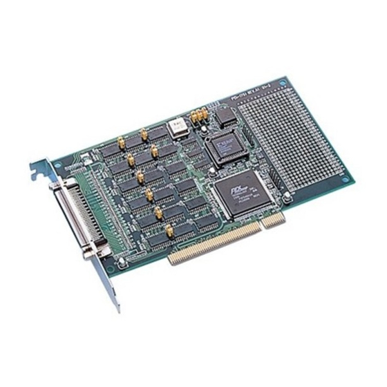
- Page 1 PCI-1751U 48-bit Digital Input/Output Card with Universal PCI Bus User Manual...
- Page 2 Acknowledgments PC-LabCard is a trademark of Advantech Co., Ltd. IBM and PC are trademarks of International Business Machines Corporation. MS-DOS and Windows are trademarks of Microsoft Corporation. Intel and Pentium are trademarks of Intel Corporation.
-
Page 3: Table Of Contents
Table 2.2:BoardID Setting (SW1) ....... 10 2.4.1 BoardID Register ............10 Table 2.3:BoardID Register ......... 10 PCI-1751U Block Diagram..........11 Figure 2.2:PCI-1751U Block Diagram ......11 Pin Assignments.............. 12 Installation Instructions ........... 13 Chapter 3 Operation ............16 Introduction ..............16 Digital I/O Ports .............. - Page 4 MODE 5 – Hardware Triggered Strobe ....... 30 Counter Operations ............31 A.4.1 Read/Write Operation ..........31 A.4.2 Counter Read-back Command ........31 A.4.3 Counter Latch Operation ..........31 Counter Applications............32 Appendix B Register Format ..........34 PCI-1751U User Manual...
- Page 5 General Information...
-
Page 6: Chapter 1 General Information
Two other features give the PCI-1751U practical advantages in an indus- trial setting. When the system is hot reset (the power is not turned off) the PCI-1751U retains the last I/O port settings and output values if the user has set jumper JA1 to enable this feature. Otherwise, port settings and output values reset to their safe default state, or to the state deter- mined by other jumper settings. -
Page 7: Applications
• High density SCSI 68-pin connector • Output status readback • Two 16-bit timers can be cascaded to one 32-bit timer, and can generate watchdog timer interrupts • One 16-bit event counter can generate event interrupts • Keeps port I/O settings and digital output states after hot system reset •... -
Page 8: Interrupt Source
• Operating temperature: 0 ~ 70º C (32º F ~ 158 ºF) • Storage temperature: -20 ~ 80º C(-4º F ~ 176º F) • Humidity: 5% ~ 95% non-condensing • Dimension: 170 x 100 mm (6.9" x 3.9") PCI-1751U User Manual... - Page 9 Installation...
-
Page 10: Chapter 2 Installation
Chapter 2 Installation 2.1 Initial Inspection Before starting to install the PCI-1751U, make sure there is no visible damage on the card. We carefully inspected the card both mechanically and electrically before shipment. It should be free of marks and in perfect order on receipt. -
Page 11: Jumper Settings
2.3 Jumper Settings We designed the PCI-1751U with ease-of-use in mind. It is a "plug and play" card, i.e. the system BIOS assigns the system resources such as base address and interrupt automatically. There are only two functions with 11 jumpers to be set by the user. The following section describes how to configure the card. -
Page 12: Using Jumpers To Set Ports As Output Ports
Jumper JA1 below.) 2.3.3 Restore Ports to Condition Prior to Reset Jumper JA1 gives the PCI-1751U a new and valuable capability. With JA1 enabled, the PCI-1751U "memorizes" all port I/O settings and output values, and, in the event of a "hot" reset, the settings and output values present at the port just prior to reset are restored to each port following reset. -
Page 13: Select Clock Source Of Timers And Counter
2.3.4 Select Clock Source of Timers and Counter Jumpers JP1, JP2 and JP3 are used to select the clock source of Timer 0, Timer 1 and Counter 2, respectively. Short the upper two pins of the jumpers to select an external clock source, or short the lower two pins to select an internal clock source. -
Page 14: Setting The Boardid Switch (Sw1)
Table 2.2. When there are multiple cards on the same chassis, this BoardID setting is useful for identifying each card's device number. We set the PCI-1751U’s BoardID switch to 0 at the factory. If you need to adjust this setting, please see below.. -
Page 15: Pci-1751U Block Diagram
2.5 PCI-1751U Block Diagram Figure 2.2: PCI-1751U Block Diagram Chapter 2... -
Page 16: Pin Assignments
Gate control pins of Counter / Timer 0, 1 and 2 INT_OUT: Interrupt output. This pin changes to logic 1 whenever PCI- 1751U generates an interrupt, and returns to logic 0 when the interrupt is cleared. GND: Ground VCC: +5 VDC voltage output PCI-1751U User Manual... -
Page 17: Installation Instructions
2.7 Installation Instructions The PCI-1751U can be installed in any PCI slot in the computer. How- ever, refer to the computer user's manual to avoid any mistakes and dan- ger before you follow the installation procedure below: Turn off your computer and any accessories connected to the com- puter. - Page 18 PCI-1751U User Manual...
- Page 19 Operation...
-
Page 20: Chapter 3 Operation
Chapter 3 Operation 3.1 Introduction This chapter describes the operating characteristics of the PCI-1751U. The driver software provided allows a user to access all of the card's func- tions without register level programming. Please see the User's Manual for the driver bundled with this card for more information. For users who... -
Page 21: Interrupt Function Of The Dio Signals
3.2.2 Interrupt Function of the DIO Signals Two I/O pins (PC00 and PC10) can be used to generate hardware inter- rupts. A user can program the interrupt control register (Base + 32) to select the interrupt sources. Refer to "Interrupt Function" in this chapter for details about interrupt control. -
Page 22: Dry Contact Support For Digital Input
Note: For wet contact configurations, a malfunction may occur if the internal resistance of the voltage source is significant (> 1.5 kW). It is advisable to connect a 1.5 kW resistor in parallel with such a voltage source to avoid a voltage rise inside the voltage source. PCI-1751U User Manual... -
Page 23: Timer/Counter Operation
3.3 Timer/Counter Operation 3.3.1 Introduction The PCI-1751U includes one 8254 compatible programmable timer/ counter chip which provides three 16-bit counters, designated as Timer 0, Timer1 and Counter 2. Each has 6 operation modes. Timer 0 and Timer 1 can be used separately or can be cascaded to create one 32-bit timer. -
Page 24: Counter 2
16-bit timer; when set as an external source, then Counter 2 is an event counter. Counter 2 is set as mode 0 (interrupt on terminal count) in the driver provided by Advantech. 3.3.4 Timer/Counter Frequency and Interrupt The input clock frequency of the counter/timers is 10 MHz. The output of both Timer 1 and Counter 2 can generate interrupts for the system (refer to section 3.3). -
Page 25: Interrupt Function
Two lines in each I/O port (C0 and C4) and two of the three counter out- puts (Timer 1 and Counter 2) are connected to the interrupt circuitry. The "Interrupt Control Register" of the PCI-1751U controls how the combina- tion of the 6 signals generates an interrupt. Two interrupt request signals can be generated at the same time, and then the software can service these two request signals by ISR. -
Page 26: Interrupt Source Control
Table 3.3: Interrupt mode bit values Port 1 Port 0 Description Description Disable interrupt Disable interrupt Source = PC10 Source = PC00 Source = PC10 & Source = PC00 & PC14 PC04 Source = Counter Source = Timer PCI-1751U User Manual... -
Page 27: Interrupt Triggering Edge Control
3.4.5 Interrupt Triggering Edge Control The interrupt can be triggered by a rising edge or a falling edge of the interrupt signal, selectable by the value written in the "triggering edge control" bit in the interrupt control register, as shown in Table 3-4. Table 3.4: Triggering edge control bit values E0 or E1 Triggering edge of interrupt signal... - Page 28 PCI-1751U User Manual...
- Page 29 Function of 8254 Counter Chip...
-
Page 30: Appendix A Counter Chip Function
1751U provides 10 MHz input frequencies to the counter chip from an on-board crystal oscillator. On the PCI-1751U, the 8254 chip's Timer 0 and Timer 1 can be used sep- arately or can be cascaded to create a 32-bit programmable timer by set- ting JP2. - Page 31 BASE+27 8254 control, standard mode Value Description: SC1 & SC0Select counter Counter Read-back command RW1 & RW0Select read/write operation Operation Counter latch Read/write LSB Read/write MSB Read/write LSB first, then MSB M2, M1 & M0Select operating mode Mode 0 programmable one shot 1 programmable one shot 2 Rate generator 3 Square wave rate generator...
- Page 32 BASE+24/25/26 Status read-back mode Value Current state of counter output Null count is 1 when the last count written to the counter register has been loaded into the counting element PCI-1751U User’s Manual...
-
Page 33: Counter Operating Modes
A.3 Counter Operating Modes A.3.1 MODE 0 – Stop on Terminal Count The output will be initially low after you set this mode of operation. After you load the count into the selected count register, the output will remain low and the counter will count. When the counter reaches the terminal count, its output will go high and remain high until you reload it with the mode or a new count value. -
Page 34: Mode 3 - Square Wave Generator
A.3.6 MODE 5 – Hardware Triggered Strobe The counter will start counting after the rising edge of the trigger input and will go low for one clock period when the terminal count is reached. The counter is retriggerable. PCI-1751U User’s Manual... -
Page 35: Counter Operations
A.4 Counter Operations A.4.1 Read/Write Operation Before you write the initial count to each counter, you must first specify the read/write operation type, operating mode and counter type in the control byte and write the control byte to the control register (BASE+27). Since the control byte register and all three counter read/write registers have separate addresses and each control byte specifies the counter it applies to (by SC1 and SC0), no instructions on the operating sequence... -
Page 36: Counter Applications
1751U interface card is a a very useful device. You can program timers 1 and 2 to serve as timers, event counters, square wave generators, or as a watchdog to generate regular interrupts at a fixed interval. PCI-1751U User’s Manual... - Page 37 Register Format of PCI-1751U...
-
Page 38: Appendix B Register Format
Reserved Reserved 8254 Counter 0 8254 Counter 0 8254 Counter 1 8254 Counter 1 8254 Counter 2 8254 Counter 2 8254 Control Register Reserved Reserved Reserved Reserved Reserved Reserved Reserved Reserved Interrupt Status Register Interrupt Control Register PCI-1751U User’s Manual...
Need help?
Do you have a question about the PCI-1751U and is the answer not in the manual?
Questions and answers