
Related Manuals for Advantech PCI-1757UP


Summary of Contents for Advantech PCI-1757UP
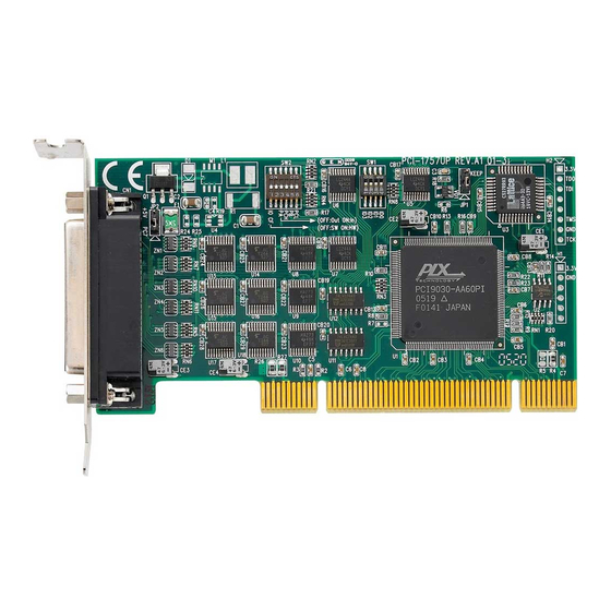
- Page 1 PCI-1757UP 24-channel Digital Input/Output Low Profile Universal PCI Card User Manual...
- Page 2 No part of this man- ual may be reproduced, copied, translated or transmitted in any form or by any means without the prior written permission of Advantech Co., Ltd. Information provided in this manual is intended to be accurate and reli- able.
- Page 3 Product Warranty (2 years) Advantech warrants to you, the original purchaser, that each of its prod- ucts will be free from defects in materials and workmanship for two years from the date of purchase. This warranty does not apply to any products which have been repaired or...
- Page 4 Step 1. Visit the Advantech web site at www.advantech.com/support where you can find the latest information about the product. Step 2. Contact your distributor, sales representative, or Advantech's cus- tomer service center for technical support if you need additional assistance. Please have the following information ready before...
-
Page 5: Table Of Contents
Contents Chapter 1 General Information ........2 Introduction ............... 2 Numbering Convention ............. 2 Features ................3 Specifications ..............4 Chapter 2 Installation ............8 Initial Inspection..............8 Unpacking ................. 8 Jumper & Switch Settings ..........8 Figure 2.1:Locations of Connectors and Jumpers ..9 2.3.1 Setting the BoardID Switch (SW1) ...... - Page 6 PCI-1757UP User Manual...
- Page 7 General Information This chapter introduces PCI-1757UP and provides detailed specifications. Sections include: • Introduction • Numbering Convention • Features • Specifications...
-
Page 8: Chapter 1 General Information
Chapter 1 General Information 1.1 Introduction PCI-1757UP is a 24-bit DI/O card with PCI bus. It provides you with 24 bits of parallel digital input/output, and emulates mode 0 of the 8255 PPI chip, but the buffered circuits offer a higher driving capability than the 8255. -
Page 9: Features
• I/O configured by software or onboard DIP switch • Hot reset output memory keeps I/O settings and digital output states after hot reset • BoardID DIP switch for multiple PCI-1757UP cards in one PC • Digital inputs with interrupt capability • D-SUB 25-pin connector... -
Page 10: Specifications
• Storage Temperature: -20 ~ 80º C (-4 ~ 176º F) • Humidity: 5 ~ 95% non-condensing • Dimensions: 119.91 x 64.41 mm (4.721" x 2.536") Low profile PCI MD1 card size. • I/O Channels: 48 digital I/O lines • Programming Mode: 8255 PPI mode 0 PCI-1757UP User Manual... - Page 11 Chapter 1...
- Page 12 PCI-1757UP User Manual...
- Page 13 Installation This chapter provides information on installing your card and making jumper/switch configurations. Sections include: • Initial Inspection • Unpacking • Jumper and Switch Settings • Pin Assignments • Installation Instructions...
-
Page 14: Chapter 2 Installation
Make sure nothing is missing. 2.3 Jumper & Switch Settings We designed PCI-1757UP with ease-of-use in mind. It is a Plug & Play card, i.e. the system BIOS assigns the system resources such as base address and interrupt automatically. The following section describes how to configure the card. -
Page 15: Figure 2.1:Locations Of Connectors And Jumpers
Figure 2.1: Locations of Connectors and Jumpers Chapter 2... -
Page 16: Setting The Boardid Switch (Sw1)
2.3.1 Setting the BoardID Switch (SW1) This section describes how to set the BoardID switch of PCI-1757UP. The figure and table below show the switch locations and how they give a unique identifier to the card. Table 2.1: BoardID Setting... -
Page 17: Output Signal At Hot Reset Setting (Jp1)
PCI-1757UP emulates one 8255 programmable peripheral interface (PPI) chip in mode 0, but with higher driving capability than a standard 8255 chip. Each of the 8255 chips has 24 programmable I/O pins that are divided into two 8-bit ports and two 4-bit ports, designated PA, PB PCL and PCH. -
Page 18: Select Pc7 Or 5V On Pin24 (Jp2)
2.3.4 Select PC7 or 5V on Pin24 (JP2) 5 V output can be output by setting JP2. Power on configuration after hot reset Pin 24 is connected to 5V Pin 24 is for PC7( Default) PCI-1757UP User Manual... -
Page 19: Pin Assignments
2.4 Pin Assignments Description of pin use: Mode Description PA0 ~ PA7 I/O pins of Port A Pin 1~8 PB0 ~ PB7 I/O pins of Port B Pin 9~16 PC0 ~ PC7 I/O pins of Port C Pin 17~24 Ground Pin 25 Chapter 2... -
Page 20: Installation Instructions
2.5 Installation Instructions PCI-1757UP can be installed in any PCI slot of the computer. However, refer to the computer user's manual to avoid any mistakes and danger before you follow the installation procedure below: Turn off your computer and any accessories connected to the com- puter. - Page 21 Operation This chapter shows how to operate PCI-1757UP. Sections include: • Overview • Digital I/O Ports • Interrupt Function • BoardID Switch...
-
Page 22: Chapter 3 Operation
Chapter 3 Operation 3.1 Overview This chapter describes how to operate PCI-1757UP. The driver software provided allows a user to access all of the card's functions without regis- ter level programming. Please see the User's Manual for the driver bun- dled with this card for more information. -
Page 23: Input/Output Control
3.2.3 Input/Output Control A control word can be written to a port's configuration register (Base+3) to set the port as an input or an output port, unless the ports are set via the switch. Table 3-1 shows the format of a control word. Table 3.1: Bit Map of Port Configuration Register Description Port C lower bits... -
Page 24: Initial Configuration
When writing to it, it is used as a control register, and when reading from it, it is used as a status register. Table 3.2: Interrupt Control Register Bit Map Bit# M0 and M1: "mode bits" of port 0 E: triggering edge control bits F: flag bits X: ignore PCI-1757UP User Manual... -
Page 25: Interrupt Source Control
3.3.2 Interrupt Source Control The "mode bits" in the interrupt control register determine the allowable sources of signals generating an interrupt. Bit 0 and bit 1 determine the interrupt source, as indicated in Figure 3-1. Table 3-3 shows the relation- ship between an interrupt source and the values in the mode bits. -
Page 26: Interrupt Flag Bit
Don't care 3.4 BoardID Switch Read Base +36 can get the cards BoardID identifier. PCI-1757UP has a built-in SMD switch (SW1), which is used to define each card’s unique identifier. You can determine this identity number in the register as shown in Table 3.6. - Page 27 Register Format...
-
Page 28: Appendix A Register Format
Appendix A Register Format Base Address Function + n (Decimal) Read Write Port A Port A Port B Port B Port C Port C Configuration Register Configuration Register Interrupt Status Register Interrupt Control Register BoardID PCI-1757UP User Manual...
Need help?
Do you have a question about the PCI-1757UP and is the answer not in the manual?
Questions and answers