Advertisement
Quick Links
Advertisement

Related Manuals for Advantech PCI-1753


Summary of Contents for Advantech PCI-1753
- Page 2 Co., Ltd. assumes no responsibility for its use, nor for any infringe- ments of the rights of third parties which may result from its use. PC-LabCard is a trademark of Advantech Co., Ltd. IBM and PC are trademarks of International Business Machines Corporation. MS- DOS and Windows are trademarks of Microsoft Corporation.
-
Page 3: Table Of Contents
Contents CHAPTER 1 General Information ......1 1.1 Introduction ............2 1.2 Features ..............4 1.3 Applications ............4 1.4 Specifications ............5 1.5 Pin Assignments ............. 6 1.6 Block Diagram ............7 CHAPTER 2 Installation ......... 9 2.1 Initial Inspection ........... 10 2.2 Unpacking ............ - Page 4 3.3.6 Interrupt Flag Bit ................... 25 3.3.7 Pattern Match Interrupt Function ............26 3.3.8 Change of State Interrupt Function ............27 APPENDIX A Register Format of PCI-1753/ 1753E ..............29 A.1 PCI-1753 Register Format ............... 30 A.2 PCI-1753E Register Format ..............31 APPENDIX B Pin Assignments of Cable PCL- 10268 ..............
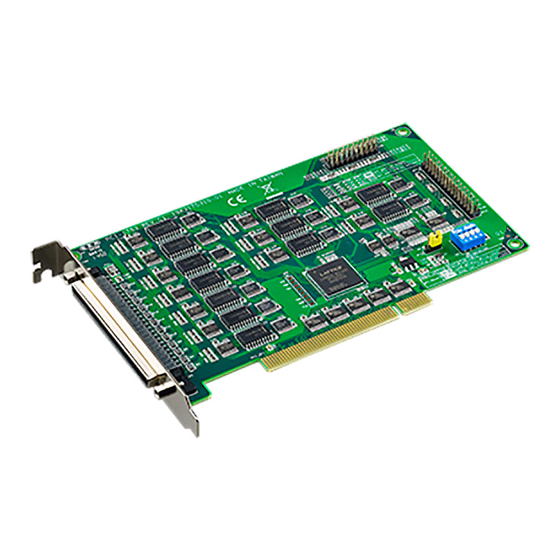
- Page 6 The PCI-1753 is a 96-bit digital I/O card for the PCI bus, which can be extended to 192 digital I/O channels by connecting with its extension board, PCI-1753E. The card emulates mode 0 of the 8255 PPI chip, but the buffered circuits offer a higher driving capability than the 8255.
- Page 7 The PCI-1753/1753E uses a 100-pin SCSI female connector. For easy signal wiring, a PCI-1753 can be connected to two ADAM-3968s by a 100-pin to 2x68-pin SCSI cable (part number PCL-10268). The ADAM-3968 allows easy access for wiring the individual pins of a 68- pin SCSI connector.
- Page 8 • High-density 100-pin SCSI connector • Industrial AC/DC I/O devices monitoring and controlling • Relay and switch monitoring and controlling • Parallel data transfer • TTL, DTL and CMOS logic signal sensing • Indicator LED driving • PCI-1753 User's Manual...
- Page 9 Operating Humidity 5 ~ 95%RH non-condensing (refer to IEC 68-2-3) Connector One 100-pin SCSI female connector PCI-1753: 175 x 100 mm (6.9" x 3.9") Dimensions PCI-1753E: 175 x 100 mm (6.9" x 3.9") MTBF over 75,013 hrs @ 25°C, ground fix environment...
- Page 10 P C 32 P C 13 P C 33 P C 14 P C 34 P C 15 P C 35 P C 16 P C 36 P C 17 P C 37 V C C V C C PCI-1753 User's Manual...
- Page 11 Figure 1-1: PCI-1753/1753E Block Diagram Chapter 1 Gerneral Information...
- Page 12 PCI-1753 User's Manual...
- Page 13 Chapter 2 Installation...
- Page 14 Before starting to install the PCI-1753/1753E, make sure there is no visible damage on the card. We carefully inspected the card both mechanically and electrically before shipment. It should be free of marks and in perfect order on receipt. As you unpack the PCI-1753/1753E, check it for signs of shipping damage (damaged box, scratches, dents, etc.).
- Page 15 We designed the PCI-1753/1753E with ease-of-use in mind. It is a "plug and play" card, i.e. the system BIOS assigns the system resourc- es such as base address and interrupt automatically. There are only two functions with 17 jumpers on the PCI-1753, and one function with 16 jumpers on the PCI-1753E.
-
Page 16: Features
(voltage low), unless jumper JP1 determines otherwise. (See Jumper JP1 below.) Jumper JP1 gives the PCI-1753/1753E a new and valuable capability. With JP1 enabled (i.e., by shorting the lower two pins of JP1), the PCI- 1753/1753E "memorizes" all port I/O settings and output values, and, in the event of a "hot"... - Page 17 Table 2-1: Summary of jumper settings Names of Jumpers Function description JPA0, JPA1, JPA2 and JPA3: Jumpers for ports A0, A1, A2 and A3 Sets port as an output port JPB0, JPB1, JPB2 and JPB3: Jumpers for ports B0, B1, B2 and B3 JPC0L, JPC1L, JPC2L and JPC3L: Jumpers for low nibble of ports C0, C1, C2 and C3 Sets port to be software...
- Page 18 Save the screw to secure the interface card retaining bracket. 5. Carefully grasp the upper edge of the PCI-1753. Align the hole in the retaining bracket with the hole on the expansion slot and align the gold striped edge connector with the expansion slot socket.
- Page 19 6. Secure the PCI-1753/1753E card by screwing the mounting bracket to the back panel of computer. 7. Attach any accessories (100-pin cable, wiring terminal board, etc.) to the card. 8. Replace the cover of your computer. Connect the cables you removed in step 2.
- Page 20 PCI-1753 User's Manual...
- Page 21 Chapter 3 Function Description...
-
Page 22: Pin Assignments
8255 chip. Each of these 8255 chip emulators has 24 programmable I/O pins that are divided into three 8- bit ports. The total 96 digital I/O pins on either the PCI-1753 or the PCI-1753E are divided into 12 ports, designated PA0, PB0, PC0, PA1, PB1, PC1, PA2, PB2, PC2, PA3, PB3 and PC3. -
Page 23: Jumper Settings
A control word can be written to a port's configuration register (Base+3, 7, 11 and 15 respectively for ports 0, 1, 2 and 3 on the PCI- 1753, and Base+35, 39, 43 and 47 respectively for ports 0, 1, 2 and 3 on the PCI-1753E) to set the port as an input or an output port, unless the ports are set as output ports via jumpers (refer to Section 2.3, Jumper Settings). - Page 24 (> 1.5 k Ω ). It is advisable to connect a 1.5 k Ω resistor in parallel with such a voltage source to avoid a voltage rise inside the voltage source. PCI-1753 User's Manual...
- Page 25 The “Interrupt Control Registers” (Base + 16, 17, 18 and 19 for the PCI-1753, and Base + 48, 49, 50 and 51 for the PCI-1753E) control the interrupt signal sources, edges and flags. The following table shows the bit map of each interrupt control register. These registers are readable/writable.
-
Page 26: Mode 0
En: triggering edge control bit (n = 0 ~ 3) Fn: interrupt flag bit of port Cn (n = 0 ~ 3) F01: pattern patch interrupt flag bit of port A0 F02: change of state interrupt flag bit of port B0 PCI-1753 User's Manual... - Page 27 M 0 1 :M 0 0 P C 0 0 P C 0 4 M 11 :M 1 0 P C 1 0 P C 1 4 V C C M 2 1 :M 2 0 P C 2 0 C L K P C 2 4 M 3 1 :M 3 0...
- Page 28 C1, and so forth. Because of sharing the same PCI controller with the PCI-1753, the PCI-1753E’s interrupt sources are also con- trolled by the PCI-1753’s interrupt control register. Bit 4 and bit 5 of Base+48 determines the interrupt source of port C0 on the PCI- 1753E, bit 4 and bit 5 of Base+49 determines the interrupt source of port C1, and so forth.
- Page 29 The interrupt can be triggered by a rising edge or a falling edge of the interrupt signal, selectable by the value written in the “triggering edge control” bit in the interrupt control register, as shown in follow- ing table. Table 3-4: Triggering edge control bit values En (n = 0 ~ 3) Triggering edge of interrupt signal Rising edge trigger...
-
Page 30: Interrupt Functions
Example 3.1 Assume that the pattern match function for the I/O channels PA01, PA02, PA06 and PA07 of the PCI-1753 is enabled (i.e. PA00, PA03, PA04 and PA05 on the PCI-1753 and port A0 on the PCI- 1753E are ignored during the pattern match monitoring process). The... - Page 31 I/O channels PB01, PB02, PB06 and PB07 on the PCI-1753E are enabled (i.e. the signals in PB00, PB03, PB04 and PB05 on the PCI- 1753E and port B0 of the PCI-1753 are ignored during the change of state process). When a change of state occurs in either PB01 or PB02 or PB06 or PB07, an interrupt signal will be delivered to the system.
- Page 32 Enable the change of state interrupt function for port A0 Disable the change of state interrupt function for port A0 c) When a change of state occurs in PB01 or PB02 or PB06 or PB07 on the PCI-1753E, an interrupt signal is generated. PCI-1753 User's Manual...
- Page 33 Appendix A Calibration...
-
Page 34: Interrupt Control Registers
Interrupt Control Register for Port 2 Interrupt Control Register for Port 2 Interrupt Control Register for Port 3 Interrupt Control Register for Port 3 Pattern Match Value Register for Port A0 Pattern Match Enable Register for Port A0 Change of State Enable Register for Port B0 PCI-1753 User's Manual... - Page 35 Base Function Address Read Write + (Decimal) Port A0 Port A0 Port B0 Port B0 Port C0 Port C0 Port 0 Configuration Register Port A1 Port A1 Port B1 Port B1 Port C1 Port C1 Port 1 Configuration Register Port A2 Port A2 Port B2 Port B2...
- Page 36 PCI-1753 User's Manual...
- Page 37 Appendix A Calibration...
- Page 38 PIN 98 PIN 99 PIN 46 PIN 96 PIN 74 PIN 75 PIN 47 PIN 97 PIN 48 PIN 98 PIN 49 PIN 99 PIN 100 PIN 50 PIN 100 * CON0, CON1 and CON2 are female Connectors PCI-1753 User's Manual...
Need help?
Do you have a question about the PCI-1753 and is the answer not in the manual?
Questions and answers