
Related Manuals for ADLINK Technology M-322


Summary of Contents for ADLINK Technology M-322
- Page 1 M-322 ATX Industrial Motherboard with Intel® Q35 Chipset User’s Manual Manual Rev.: 2.02 Revision Date: Mar 23, 2011 Part No: 50-1Z052-1020 Advance Technologies; Automate the World.
-
Page 2: Revision History
Revision History Revision Release Date Description of Change(s) 2.00 2010/06/23 Initial Release 2.01 2010/09/27 Correct System Panel Pin Header drawing 2.02 2011/05/23 Correct misc. typos; update addresses... -
Page 3: Preface
M-322 Preface Copyright 2010-2011 ADLINK Technology Inc. This document contains proprietary information protected by copy- right. All rights are reserved. No part of this manual may be repro- duced by any mechanical, electronic, or other means in any form without prior written permission of the manufacturer. - Page 4 Using this Manual Audience and Scope The M-322 User’s Manual is intended for hardware technicians and systems operators with knowledge of installing, configuring and operating industrial grade computers. Manual Organization This manual is organized as follows: Preface: Presents copyright notifications, disclaimers, trade- marks, and associated information on the proper usage of this document and its associated product(s).
- Page 5 M-322 Conventions Take note of the following conventions used throughout this manual to make sure that users perform certain tasks and instructions properly. Additional information, aids, and tips that help users perform tasks. NOTE: NOTE: Information to prevent minor physical injury, component dam- age, data loss, and/or program corruption when trying to com- plete a task.
- Page 6 This page intentionally left blank. Preface...
-
Page 7: Table Of Contents
M-322 Table of Contents Revision History..............ii Preface ..................iii List of Figures ................ xi List of Tables................ xiii 1 Introduction ................ 1 Package Contents ............... 1 Overview................2 Features................2 Specifications............... 3 Power Consumption ............5 Block Diagram ..............6 Functional Description ............ - Page 8 4 BIOS Setup ................ 37 Starting the BIOS ............... 37 Main Setup................. 41 Advanced Setings .............. 45 4.3.1 USB Configuration ............46 4.3.2 Trusted Computing ............48 4.3.3 Intel TXT (LT) Configuration .......... 49 4.3.4 Intel VT-d Configuration..........49 4.3.5 CPU Configuration............50 4.3.6 Chipset Settings.............
- Page 9 M-322 Important Safety Instructions ..........77 Getting Service..............79 Table of Contents...
- Page 10 This page intentionally left blank. Table of Contents...
-
Page 11: List Of Figures
List of Figures Figure 1-1: M-322 Block Diagram ............6 Figure 1-2: M-322 Board Layout ............9 Figure 1-3: M-322 Rear I/O Layout ..........10 Figure 1-4: M-322 Board Dimensions ..........11 Figure 1-5: M-322 I/O Shield Dimensions ........12... - Page 12 This page intentionally left blank. List of Figures...
-
Page 13: List Of Tables
M-322 List of Tables Table 1-1: M-322 General Specifications.......... 4 Table 1-2: M-322 Board Layout Legend ......... 10 Table 2-1: COM Serial Port Connector Pin Definition..... 14 Table B-1: System Memory Map............. 67 Table B-2: Direct Memory Access Channels........68 Table B-3: Fixed I/O Map .............. - Page 14 This page intentionally left blank. List of Tables...
-
Page 15: Introduction
M-322 Introduction This chapter will introduce the M-322, its features, specifications, functional description, and mechanical layout. 1.1 Package Contents Please check that your package contains the items below. If you discover damaged or missing items, please contact your vendor. M-322 Industrial ATX Motherboard... -
Page 16: Overview
1333 MHz Front Side Bus (FSB). Dual channel DDR2 667/800 MHz memory is supported up to a maximum of 8GB in four DIMM slots. The M-322 supports a broad range of processor frequencies, high-speed data transfer rates, diverse I/O functions, and high-bandwidth network connectivity. -
Page 17: Specifications
M-322 1.4 Specifications System CPU/Cache • IIntel® Core™2 Quad Q9400, 2.66GHz, 1333MHz FSB, 6MB L2 Cache, 45nm, 95W TDP • Intel® Core™2 Duo E8400, 3.0GHz, 1333MHz FSB, 6MB L2 Cache, 45nm, 65W TDP • Intel® Core™2 Duo E7400, 2.8GHz, 1066MHz FSB, 3MB L2 Cache, 45nm, 65W TDP •... -
Page 18: Table 1-1: M-322 General Specifications
• 305 mm x 244 mm (L x W) Operating Temp. • 0°C to 60°C Storage Temp. • -20ºC to 80ºC Rel. Humidity • 10 - 90% non-condensing Safety • CE, FCC Class A Table 1-1: M-322 General Specifications Introduction... -
Page 19: Power Consumption
M-322 1.5 Power Consumption Intel® Core™2 Duo Processor E6400 Test Configuration Intel® Core™2 Duo Processor E6400 2.13 GHz Memory ADATA DDR2 667 1G (AD2667001GOU) x1 Graphics Intel ® Q35 Graphics Memory Controller Hub Hard Drive Seagate Barracuda 7200.10 160GB ST3160815AS Power Supply Delta 400W, GPS-400AB C Rev. -
Page 20: Block Diagram
PCI Express x1 6x SATA ports 12x USB 2.0 USB 2.0 PCI Bus (4x Bracket, 8x Internal) Controller 32-bit/33MHz bus Codec Realtek ALC888 SPI BIOS KB/Mouse Winbond LPT/FDD 83627 DHG-A Super I/O 1x RS-232/422/485 3x RS-232 Figure 1-1: M-322 Block Diagram Introduction... -
Page 21: Functional Description
M-322 1.7 Functional Description Processor Support The M-322 is designed for Intel Yorkfield/Wolfdale/Conroe quad, dual and single core processors in LGA775 socket with core fre- quencies from 1.8 GHz up to 3.0 GHz. The CPU connects with the Intel® Q35 GMCH through a 2 GB/s DMI interface. - Page 22 Serial ATA Storage is efficient and secure with the Serial ATA interface. Utiliz- ing the Intel® ICH9DO, the M-322 supports up to six Serial ATA devices capable of reading/writing data at up to 3 Gbps. Intel® Matrix Storage Technology provides support for RAID 0/1/5/10.
-
Page 23: Board Layout
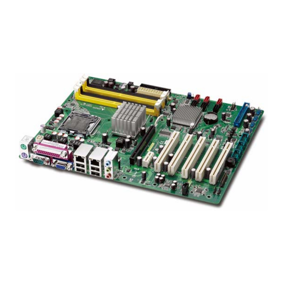
M-322 1.8 Board Layout ATX12V CPU_FAN JCOMPWR1 DIMM_A1 DIMM_A2 DIMM_B1 DIMM_B2 PWR_FAN FLOPPY EATXPWR PCIEX16 CLRTC PCIEX1_1 CHASSIS SATA1-6 PCI1-5 CD-IN CHA_FAN1 F_PANEL AAFP PRI_EIDE JAMP1 SPDIF_OUT JDIO COM2 COM3 COM4 USB56/78/910/1112 JCOMPWR2-7 Figure 1-2: M-322 Board Layout Introduction... -
Page 24: Figure 1-3: M-322 Rear I/O Layout
DIMM_B1/B2 240-pin DIMM slots (Channel B) PCIEX1_1 PCI express x1 slot PCIEX16 PCI express x16 slot PCI1-5 PCI slots Table 1-2: M-322 Board Layout Legend Parallel PS/2 KB/MS COM1 Audio LAN + USB Figure 1-3: M-322 Rear I/O Layout Introduction... -
Page 25: Mechanical Drawings
M-322 1.9 Mechanical Drawings Dimensions in mm Figure 1-4: M-322 Board Dimensions Introduction... -
Page 26: Figure 1-5: M-322 I/O Shield Dimensions
Dimensions in mm Figure 1-5: M-322 I/O Shield Dimensions Introduction... -
Page 27: Connectors & Jumpers
M-322 Connectors & Jumpers The connectors and jumpers on the M-322 allow you to connect and configure external devices. The following specify the pin assignments for connectors and jumper on the M-322. Refer to Figure 1-2: M-322 Board Layout and Figure 1-3: M-322 Rear I/O Layout for connector and jumper locations. -
Page 28: Table 2-1: Com Serial Port Connector Pin Definition
COM DB-9 Serial Port Connector Pin # RS-232 DCD, Data carrier detect RXD, Receive data TXD, Transmit data DTR, Data terminal ready GND, ground DSR, Data set ready RTS, Request to send CTS, Clear to send RI, Ring indicator Table 2-1: COM Serial Port Connector Pin Definition VGA Connector. -
Page 29: Parallel Port
M-322 Parallel Port. Pin # Signal Name Pin # Signal Name STROBE AUTO FEED DATA0 ERROR DATA1 INIT DATA2 SELECT IN DATA3 DATA4 DATA5 DATA6 DATA7 ACKNOWLEDGE BUSY PAPER EMPTY SELECT USB Connectors Pin # Signal Name USB- USB+ Connectors & Jumpers... - Page 30 LAN (RJ-45) Ports 10BASE-T/ Pin # 1000BASE-T 100BASE-TX BI_DA+ BI_DA- LED1 LED2 BI_DB+ BI_DC+ BI_DC- BI_DB- BI_DD+ BI_DD- Refer to the table below for the LAN port LED definitions. LED1 (ACT/Link) LED2 (Speed) Status Description Status Description No Link 10 Mb/s Orange Linked Orange...
-
Page 31: Onboard Connectors
M-322 2.2 Onboard Connectors Front Panel Audio Pin Header (AAFP) Pin # Signal Pin # Signal MIC2_L AGND MIC2_R FP_PRES# MIC2_R SRTN1 SENSE A LIN2_L SRTN2 ATX 12V Power Connector (ATX12V) Pin # Signal +12V DC +12V DC ATX Power Connector (EATXPWR) - Page 32 CD-in Connector (CD) Pin # Signal Left Audio Channel CD_GND CD_GND Right Audio Channel System Fan Connector (CHA_FAN1) Pin # Signal Fan Sense Fan Power (+12V) CPU Fan Connector (CPU_FAN) Pin # Signal Fan Power (+12V) Fan Sense Fan Speed Control Chassis Intrusion Connector (CHASSIS) Pin # Signal...
- Page 33 M-322 Serial Port Connectors RS-232 (COM2-4) Pin # RS-232 DCD, Data carrier detect RXD, Receive data TXD, Transmit data DTR, Data terminal ready GND, ground DSR, Data set ready RTS, Request to send CTS, Clear to send RI, Ring indicator...
- Page 34 Floppy Disk Drive Connector (FLOPPY) Pin # Signal Pin # Signal Extended Density Index Motor A Select Drive A Select Step Direction Step Pulse Write Data Write Gate Track 0 Write Protect Read Data Head Select Disk Change System Panel Pin Header (F_PANEL) Pin # Signal Pin Group...
- Page 35 M-322 Amplifier Audio Pin Header (JAMP1) Pin # Signal AMP_L- AMP_L+ AMP_R- AMP_R+ Digital IO Pin Header (JDIO) Pin # Signal Pin # Signal DIO GP20 DIO GP10 DIO GP21 DIO GP11 DIO GP22 DIO GP12 DIO GP23 DIO GP13...
- Page 36 IDE Connector (PRI_EIDE) Pin # Signal Pin # Signal Reset Ground Data 7 Data 8 Data 6 Data 9 Data 5 Data 10 Data 4 Data 11 Data 3 Data 12 Data 2 Data 13 Data 1 Data 14 Data 0 Data 15 Ground Request...
- Page 37 M-322 SATA Connectors (SATA1-6) Pin # Signal S/PDIF Pin Header (SPDIF_OUT) Pin # Signal – SPDIF0 SPI Pin Header (SPI) Pin # Signal Pin # Signal +3V ROM F_SPI_CS# F_SPI_CLK F_SPI_MISO F_SPI_MOSI – USB Pin Headers (USB56/78/910/1112) Pin # Signal...
-
Page 38: Jumpers
The CMOS RAM data contains the date/time and BIOS setting information. CMOS is powered by the onboard button cell battery. To erase the CMOS RAM data: 1. Disconnect power from the M-322 2. Short the CLRTC pins 2-3 3. Turn the power on. After power on, remove the jumper cap from pins 2-3 and reinstall it to pins 1-2. - Page 39 M-322 COM4 RS-232/422/485 Select (JCOMPWR5, 6, 7) Short the jumper pins according to the following settings to set COM4 to RS-232/422/485 mode. JCOMPWR5 JCOMPWR6/7 RS-232 RS-422 RS-485 Connectors & Jumpers...
- Page 40 This page intentionally left blank. Connectors & Jumpers...
-
Page 41: Getting Started
This chapter provides information on how to install components to the M-322 motherboard. 3.1 Installing the CPU The M-322 Supports the Intel® Core™2 Duo/Quad, Intel® Pen- tium® Dual-Core, and Intel® Celeron® processors via the surface mount LGA775 socket (Socket T). - Page 42 2. Lift and rotate the load lever to a 135° angle 3. Lift the load plate to a 100° angle using your thumb and forefinger 4. Use your thumb to push and remove the protective socket cover (plastic) from the load plate Getting Started...
- Page 43 M-322 5. Position the CPU over the socket, then match the notches on the CPU side with the alignment keys on the socket. The golden triangle on the CPU must be posi- tioned on the bottom-left corner of the socket .
- Page 44 7. Close the load plate (A), then fasten the load lever on the retention tab (B) . Getting Started...
-
Page 45: Installing The Cpu Fan And Heatsink
Failure to install a CPU fan and heatsink may damage the motherboard and/or the CPU. The following CPU fan and heatsink assembly is recommended for use with the M-322: Copper-Core Cooler Dimensions: 115 x 115 x 61.4 mm Heatsink: Aluminum extrusion+copper core Fan speed: 4500 RPM Fan airflow: 76.9 CFM... -
Page 46: System Memory
3.3 System Memory The M-322 supports up to 8 GB of DDR2 667/800 MHz memory modules in four DIMM sockets. DDR2 modules are notched to facilitate correct installation in the DIMM sockets. See Figure 1-2 on page 9 for DIMM socket locations. - Page 47 M-322 To install a memory module: 1. Locate the DIMM slots on the motherboard. 2. Press the socket’s retaining clips outward to unlock. 3. Align the memory module on the socket making sure that the notch matches the break on the socket.
-
Page 48: Driver Installation
3.4 Driver Installation This section provides information on how to install the M-322 device drivers under Windows XP. The device drivers are located in the following directories on the driver CD, or can be downloaded from the ADLINK website (http://www.adlinktech.com):... - Page 49 M-322 Intel Q35 Express Chipset Driver ® This section describes the installation of the Intel® Q35 Express chipset driver. 1. Locate the directory X:\Drv_Chipset_Q35\. 2. Run the program setup.exe and follow the onscreen instructions. Restart the system if prompted. Display Driver Follow these instructions to install the display driver: 1.
- Page 50 Intel® Matrix Storage Manager Follow these instructions to install the Intel® Matrix Storage Manager utility. 1. Locate the directory X:\Intel Matrix Storage Manager\ on the driver CD. 2. Run the program iata78_enu.exe and follow the onscreen instructions. Restart the system if prompted. TPM Driver Follow these instructions to install the TPM driver.
-
Page 51: Bios Setup
M-322 BIOS Setup The following chapter describes basic navigation for the AMIBIOS®8 BIOS setup utility. 4.1 Starting the BIOS To enter the setup screen, follow these steps: 1. Power on the motherboard 2. Press the < Delete > key on your keyboard when you see the following text prompt: <... - Page 52 Setup Menu The main BIOS setup menu is the first screen that you can navi- gate. Each main BIOS setup menu option is described in this user’s guide. The Main BIOS setup menu screen has two main frames. The left frame displays all the options that can be configured.
- Page 53 M-322 Note: There is a hot key legend located in the right frame on most setup screens. The < F8 > key on your keyboard is the Fail-Safe key. It is not dis- played on the key legend by default. To set the Fail-Safe settings of the BIOS, press the <...
- Page 54 The < F10 > key allows you to save any changes you have made and exit Setup. Press the < F10 > key to save your changes. The following screen will appear: Press the < Enter > key to save the configuration and exit. You can also use the <...
-
Page 55: Main Setup
M-322 4.2 Main Setup When you first enter the Setup Utility, you will enter the Main setup screen. You can always return to the Main setup screen by select- ing the Main tab. There are two Main Setup options. They are described in this section. - Page 56 Floppy A Sets the type of floppy drive installed. Options: [Disabled], [360KB, 5 1/4], [1.2MB, 5 1/4], [720KB, 5 1/ 4], [1.44MB, 5 1/4], [2.88MB, 3 1/2] SATA 1~6 The BIOS automatically detects the presence of SATA devices. There is a separate sub-menu for each IDE device. Select a device item then press <Enter>...
- Page 57 M-322 SATA Configuration SATA Configuration Allows you to disable or enable SATA Configuration function. Options: [Disabled], [Compatible], [Enhanced] Configure SATA as Configures the Serial ATA connectors supported by the South- bridge chip. The AHCI allows the onboard storage drive to...
- Page 58 AHCI Settings System Information BIOS Setup...
-
Page 59: Advanced Setings
M-322 4.3 Advanced Setings Select the Advanced tab from the setup screen to enter the Advanced BIOS Setup screen. You can select any of the items in the left frame of the screen to go to the sub menu for that item. -
Page 60: Usb Configuration
4.3.1 USB Configuration You can use this screen to select options for the USB Configura- tion. Select an item then press <Enter> to display the configuration options. USB Functions Allows you to enable or disable USB functions. Options: [Disabled], [Enabled] Legacy USB Support [Enabled] Allows you to enable or disable support for USB devices on legacy operating systems (OS). - Page 61 M-322 USB 2.0 Controller Allows you to enable or disable the USB 2.0 controller. Options: [Enabled], [Disabled]. BIOS EHCI Hand-Off Allow you to enable support for operating systems without an EHCI hand-off feature. Options: [Disabled], [Enabled]. Port 64/60 Emulation Allows you to disable or enable the I/O port 60h/64h emulation support.
-
Page 62: Trusted Computing
4.3.2 Trusted Computing Trusted computing is an industry standard to make personal com- puters more secure through a dedicated hardware chip, called a Trusted Platform Module (TPM). This option enables or disables the TPM support. BIOS Setup... -
Page 63: Intel Txt (Lt) Configuration
M-322 4.3.3 Intel TXT Configuration Allows you to enable or disable Intel® Trusted Execution Technology initialization. Options: [Disabled], [Enabled] 4.3.4 Intel VT-d Configuration Allows you to enable or disable Intel® Virtualization Technology. Options: [Disabled], [Enabled] BIOS Setup... -
Page 64: Cpu Configuration
4.3.5 CPU Configuration You can use this screen to select options for the CPU Configura- tion Settings. Hardware Prefetcher Options: [Enabled], [Disabled]. Adjacent Cache Line Prefetch Options: [Enabled], [Disabled]. Max CPUID Value Limit Setting this item to [Enabled] allows legacy operating systems without support for CPUs with extended CPUID functions to boot. - Page 65 M-322 Execute Disable Bit Allows you to enable or disable the No-Execution Page Protec- tion Technology. Setting this item to [Disabled] forces the XD feature flag to always return a zero (0). Options: [Enabled], [Disabled]. Intel SpeedStep Tech Options: [Enabled], [Disabled].
-
Page 66: Chipset Settings
4.3.6 Chipset Settings The Chipset menu allows you to change the advanced chipset set- tings. Select an item then press <Enter> to display the sub-menu. North Bridge Configuration Memory Remap Feature Allows you to enable or disable the remapping of the over- lapped PCI memory above the total physical memory. - Page 67 M-322 Internal Graphic Mode Select Allows you to select the amount of system memory used by the Internal Graphics Device. Options: [Disabled], [Enabled,1MB], [Enabled, 8MB] PEG Port Control Allows you to disable or enable PEG port control. Options: [Auto], [Disabled]...
-
Page 68: Onboard Device Configuration
4.3.7 Onboard Device Configuration Onboard LAN Boot Options: [Enabled], [Disabled] JMicron 36X ATA Controller Allows you to enable or disable the JMicron 36X ATA controller (PATA function). Options: [Enabled], [Disabled]. Serial Port Address Allow you to select the Serial Port base address. Options: [Disabled], [3F8], [2F8], [3E8], [2E8] Serial Port IRQ Options: [3], [4], [10], [11]... -
Page 69: Pci/Pnp Settings
M-322 Parallel Port Mode Allow you to select the Parallel Port mode. Options: [Normal], [Bi-Directional], [ECP], [EPP], [ECP&EPP] Parallel Port IRQ Options: [IRQ5], [IRQ7] 4.3.8 PCI/PnP Settings When set to [No], BIOS configures all the devices in the system. When set to [Yes] and if you install a Plug and Play operating sys- tem, the operating system configures the Plug and Play devices not required for boot. -
Page 70: Power Settings
4.4 Power Settings The Power menu items allow you to change the settings for the Power Management. Select an item then press <Enter> to display the configuration options. Suspend Mode Allows you to select the Advanced Configuration and Power Inter- face (ACPI) state to be used for system suspend. - Page 71 M-322 ACPI Version Features Allows you to add more tables for Advanced Configuration and Power Interface (ACPI) 2.0 specifications. Options: [ACPI V1.0], [ACPI V2.0], [ACPI V3.0] ACPI APIC Support [Enabled] Allows you to enable or disable the Advanced Configuration and Power Interface (ACPI) support in the Application-Specific Inte- grated Circuit (ASIC).
-
Page 72: Apm Configuration
4.4.1 APM Configuration Restore on AC Power Loss Determines which state the computer enters when AC power is restored after a power loss. The options for this value are Last State, Power On and Power Off. Power Off: Set this value to always power off the system while AC power is restored. -
Page 73: Hardware Health Configuration
M-322 4.4.2 Hardware Health Configuration This submenu displays system health information (temperatures, voltages, fan speeds) and allows CPU Smart Fan Profile configu- ration. CPU Smart Fan Profile Allows you to select the CPU FAN profile mode. Silent Mode: Keeps system at quieter than Optimized Mode with lower fan speed. -
Page 74: Boot Settings
4.5 Boot Settings The Boot Settings menu allows you to change the system boot options. Select an item and press <Enter> to display the submenu. 4.5.1 Boot Device Priority The items allow you to set the sequence of boot devices where BIOS attempts to load the disk operating system. -
Page 75: Boot Settings Configuration
M-322 4.5.3 Boot Settings Configuration Quick Boot Enabling this setting will cause the BIOS power-on self test routine to skip some of its tests during bootup for faster system boot. Options: [Disabled], [Enabled] Quiet Boot When this feature is enabled, the BIOS will display the full- screen logo during the boot-up sequence, hiding normal POST messages.When it is disabled, the BIOS will display the normal... -
Page 76: Security
Wait for ‘F1’ If Error When set to Enabled, the system waits for the F1 key to be pressed when an error occurs. Options: [Disabled], [Enabled]. Hit ‘DEL’ Message Display The system displays the message “Press DEL to run Setup” during POST when set to Enabled. -
Page 77: Exit Menu
M-322 4.6 Exit Menu Select the Exit tab from the setup screen to enter the Exit BIOS Setup screen. You can display an Exit BIOS Setup option by high- lighting it using the < Arrow > keys. The Exit BIOS Setup screen is shown below. - Page 78 Discard Changes and Exit Select this option to quit Setup without making any permanent changes to the system configuration. Discard Changes and Exit Setup Now? [Ok] [Cancel] appears in the window. Select Ok to discard changes and exit. Discard Changes Select Discard Changes from the Exit menu and press <...
-
Page 79: A Appendix: Watchdog Timer
M-322 Appendix A - Watchdog Timer The following is a sample program for configuring the M-322’s watchdog timer. A.1 Sample Code Unlock W83627DHG-A: outportb(0x2E, 0x87) ;Unlock Super I/O Select Logical Device: outportb(0x2E, 0x07) ;Select device number register outportb(0x2F, 0x08) ;Set to Logical Device 8... - Page 80 This page intentionally left blank. Watchdog Timer...
-
Page 81: B Appendix: System Resources
M-322 Appendix B - System Resources B.1 System Memory Map Address Range Address Range Size Description (decimal) (hex) FFE00000 – (4GB-2MB) 2 MB High BIOS Area FFFFFFFF (4GB-18MB) – FEE00000 – 1 MB FSB Interrupt Memory Space (4GB-17MB-1) FEEFFFFF (4GB-20MB) –... -
Page 82: Direct Memory Access Channels
B.2 Direct Memory Access Channels Channel Number Data Width System Resource 8-bits Parallel port 8-bits Parallel port 8-bits Diskette drive 8-bits Parallel port Reserved - cascade channel 16-bits Open 16-bits Open 16-bits Open Table B-2: Direct Memory Access Channels System Resources... -
Page 83: Fixed I/O Map
M-322 B.3 Fixed I/O Map Hex Range Device 00h-08h DMA Controller 09h-0Eh RESERVED DMA Controller 10h-18h DMA Controller 19h-1Eh RESERVED DMA Controller 20h-21h Interrupt Controller 24h-25h Interrupt Controller 28h-29h Interrupt Controller 2Ch-2Dh Interrupt Controller 2E-2F LPC SIO 30h-31h Interrupt Controller... -
Page 84: Table B-3: Fixed I/O Map
Hex Range Device RTC Controller RTC Controller DMA Controller and LPC or PCI 81h-83h DMA Controller 84h-86h DMA Controller DMA Controller DMA Controller 89h-8Bh DMA Controller 8Ch-8Eh DMA Controller 08Fh DMA Controller 90h-91h DMA Controller Reset Generator (Processor I/F) 93h-9Fh DMA Controller A0h-A1h Interrupt Controller... -
Page 85: Variable I/O Map
M-322 B.4 Variable I/O Map Hex Range Device Anywhere in 64 KB I/O Space ACPI Anywhere in 64 KB I/O Space IDE Bus Master Anywhere in 64 KB I/O Space Native IDE Command Anywhere in 64KB I/O Space Native IDE Control... -
Page 86: Interrupt Request (Irq) Lines
B.5 Interrupt Request (IRQ) Lines IRQ Lines PIC Mode Typical Interrupt IRQ# Connected to Pin Resource Internal Timer / Counter 0 output / System timer HPET #0 Communications Port IRQ3 via SERIRQ, PIRQ# (COM2) Communications Port IRQ4 via SERIRQ, PIRQ# (COM1) Floppy Disk IRQ6 via SERIRQ, PIRQ#... - Page 87 M-322 IRQ Lines APIC Mode IRQ# Typical Interrupt Resource Connected to Pin Internal Timer / Counter 0 output / System timer HPET #0 Communications Port (COM2) IRQ3 via SERIRQ, PIRQ# Communications Port (COM1) IRQ4 via SERIRQ, PIRQ# Floppy Disk IRQ6 via SERIRQ, PIRQ#...
-
Page 88: Table B-6: Irq Lines Apic Mode
IRQ# Typical Interrupt Resource Connected to Pin Intel ICH9 Family PCI Express Root Port 3 – 2944 Intel ICH9 Family USB Universal Host Controller – 2936 Intel ICH9 Family USB2 Enhanced Host Controller – 293C Realtek RTL8168C(P)/8111C(P) PCI-E Gigabit Ethernet NIC Intel ICH9 2 port Serial ATA Storage Controller 2 - 2926 Intel ICH9 Family USB Universal... -
Page 89: Pci Configuration Space Map
M-322 B.6 PCI Configuration Space Map Bus # Device # Function # Routing Description Intel host bridge Internal Intel VGA controller Internal Intel USB UHCI Internal Intel USB UHCI Internal Intel USB UHCI Internal Intel USB UHCI Internal Intel Internal... -
Page 90: Pci Interrupt Routing Map
B.7 PCI Interrupt Routing Map INT Line INT0 INT1 INT2 INT3 Intel VGA controller Intel USB UHCI Intel USB UHCI Intel USB UHCI Intel USB UHCI Intel unknow device Intel PCI/PCI bridge Intel PCI/PCI bridge Intel PCI/PCI bridge Intel PCI/PCI bridge Intel USB UHCI Intel USB UHCI Intel USB UHCI... -
Page 91: Important Safety Instructions
M-321 Important Safety Instructions For user safety, please read and follow all instructions, WARNINGS, CAUTIONS, and NOTES marked in this manual and on the associated equipment before handling/operating the equipment. Read these safety instructions carefully. Keep this user’s manual for future reference. Read the specifications section of this manual for detailed information on the operating environment of this equipment. - Page 92 Never attempt to fix the equipment. Equipment should only be serviced by qualified personnel. A Lithium-type battery may be provided for uninterrupted, backup or emergency power. Risk of explosion if battery is replaced with one of an incorrect type. Dispose of used batteries appropriately. WARNING: Equipment must be serviced by authorized technicians when:...
-
Page 93: Getting Service
Address: 5215 Hellyer Avenue, #110, San Jose, CA 95138, USA Tel: +1-408-360-0200 Toll Free: +1-800-966-5200 (USA only) Fax: +1-408-360-0222 Email: info@adlinktech.com ADLINK Technology (China) Co., Ltd. Address: (201203) 300 Fang Chun Rd., Zhangjiang Hi-Tech Park, Pudong New Area, Shanghai, 201203 China Tel: +86-21-5132-8988 Fax:... - Page 94 Address: 84 Genting Lane #07-02A, Cityneon Design Centre, Singapore 349584 Tel: +65-6844-2261 Fax: +65-6844-2263 Email: singapore@adlinktech.com ADLINK Technology Singapore Pte. Ltd. (Indian Liaison Office) Address: No. 1357, "Anupama", Sri Aurobindo Marg, 9th Cross, JP Nagar Phase I, Bangalore - 560078, India Tel: +91-80-65605817 Fax: +91-80-22443548 Email: india@adlinktech.com...
Need help?
Do you have a question about the M-322 and is the answer not in the manual?
Questions and answers