Table of Contents

Related Manuals for ADLINK Technology MI-110


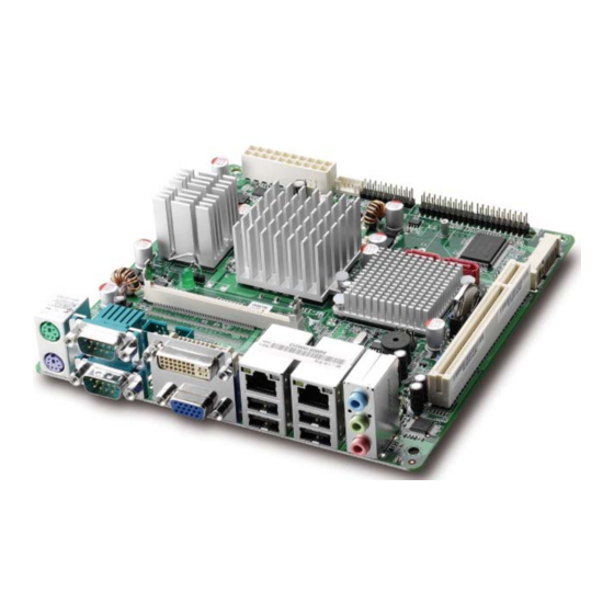
Summary of Contents for ADLINK Technology MI-110
- Page 1 MI-110 Mini-ITX Embedded Motherboard with Intel® Atom™ Processor N270 and Intel® 945GSE/ICH7M Chipset User’s Manual Manual Rev.: 2.00 Revision Date: October 2, 2009 Part No: 50-1Z012-1000 Advance Technologies; Automate the World.
-
Page 2: Revision History
Revision History Revision Release Date Description of Change(s) 2.00 2009/10/02 Initial Release... -
Page 3: Preface
MI-110 Preface Copyright 2009 ADLINK Technology Inc. This document contains proprietary information protected by copy- right. All rights are reserved. No part of this manual may be repro- duced by any mechanical, electronic, or other means in any form without prior written permission of the manufacturer. - Page 4 Using this Manual Audience and Scope The MI-110 User’s Manual is intended for hardware technicians and systems operators with knowledge of installing, configuring and operating industrial grade computers. Manual Organization This manual is organized as follows: Preface: Presents copyright notifications, disclaimers, trade- marks, and associated information on the proper usage of this document and its associated product(s).
- Page 5 MI-110 Conventions Take note of the following conventions used throughout this manual to make sure that users perform certain tasks and instructions properly. Additional information, aids, and tips that help users perform tasks. NOTE: NOTE: Information to prevent minor physical injury, component dam- age, data loss, and/or program corruption when trying to com- plete a task.
- Page 6 This page intentionally left blank. Preface...
-
Page 7: Table Of Contents
MI-110 Table of Contents Revision History..............ii Preface ..................iii Table of Contents..............vii List of Figures ................ ix List of Tables................xi 1 Introduction ................ 1 Package Contents ............... 1 Overview................2 Features................2 Specifications............... 3 Block Diagram ..............5 Functional Description ............ - Page 8 Standard CMOS Features ..........35 Advanced BIOS Features ..........37 Advanced Chipset Features..........42 Integrated Peripherals............44 Power Management Setup ..........51 PnP/PCI Configurations ............. 54 PC Health Status ............... 56 Frequency/Voltage Control ..........57 4.10 Load Optimized Defaults............ 58 4.11 Set Supervisor &...
-
Page 9: List Of Figures
List of Figures Figure 1-1: MI-110 Block Diagram ............. 5 Figure 1-2: MI-110 Board Layout ............. 10 Figure 1-3: MI-110 Rear I/O Layout ..........11 Figure 1-4: MI-110 Board Dimensions ..........12 Figure 1-5: Rear I/O Faceplate Dimensions........13 List of Figures... - Page 10 This page intentionally left blank. List of Figures...
-
Page 11: List Of Tables
List of Tables Table 1-1: MI-110 General Specifications......... 4 Table 1-2: Intel® Atom™ N270 processor Power Consumption ..9 Table 1-3: MI-110 Board Layout Legend ........11 Table B-1: System Memory Map............. 65 Table B-2: Direct Memory Access Channels........66 Table B-3: Fixed I/O Map .............. - Page 12 This page intentionally left blank. List of Tables...
-
Page 13: Introduction
MI-110 Introduction This chapter will introduce the MI-110, its features, specifications, functional description, and mechanical layout. 1.1 Package Contents Please check that your package contains the items below. If you discover damaged or missing items, please contact your vendor. MI-110 Mini-ITX Embedded Motherboard... -
Page 14: Overview
Intel® Atom™ processor N270 built on 45-nm process technology in Micro-FCBGA8 package and the Mobile Intel® 945GSE + ICH7M Express Chipset. The MI-110 is ideal for embedded applications requiring fanless operation and ultra-low power consumption in a standard small form factor motherboard with a complete set of I/O functions and high-bandwidth network connectivity. -
Page 15: Specifications
MI-110 1.4 Specifications System Intel® Atom™ processor N270 • 1.6 GHz core frequency • 512KB L2 cache • Micro-FCBGA8 package • 533 MHz Chipset • Mobile Intel® 945GSE + ICH7M Express Chipset Memory • DDR2 533 SDRAM (2GB max.) • 1x 200-pin SO-DIMM slot BIOS •... -
Page 16: Table 1-1: Mi-110 General Specifications
• 170 mm x 170 mm (L x W) Operating Temp. • 0°C to 60°C Storage Temp. • -40ºC to 80ºC Rel. Humidity • 10 - 90% RH Safety • CE, FCC Class A Table 1-1: MI-110 General Specifications Introduction... -
Page 17: Block Diagram
USB 2.0 PCI 32-bit/ PCI Bus (Bracket x4, Internal x2) Controller AC97 33MHz bus Realtek ALC888 Audio Jacks Line-in, Line-out, Mic-in Audio Codec KB/Mouse SPI BIOS KB/Mouse Winbond W83627DHG-A Hardware LPC Super I/O RS-232x4 Monitor Figure 1-1: MI-110 Block Diagram Introduction... -
Page 18: Functional Description
Enhanced low-power sleep states (C1E, C2E, C4E) Dynamic L2 cache sizing Mobile Intel® 945GSE Express Chipset The MI-110 is based on the Mobile Intel® 945GSE Express Chipset, consisting of the Intel® 82945GSE Graphics Memory Controller Hub and Intel® I/O Controller Hub 7-M. The chipset fea- tures power-efficient graphics with an integrated 32-bit 3D graph- ics engine based on Intel®... - Page 19 Gigabit Ethernet The MI-110 is equipped with the PCI Express Realtek 8111C GbE controller. Serial ATA Storage is efficient and secure with the Serial ATA interface. Utiliz- ing the Intel®...
- Page 20 Watchdog Timer The watchdog timer (WDT) monitors system operations based on user-defined configurations. The WDT can be programmed for dif- ferent time-out periods, such as from 1 to 255 seconds or from 1 to 255 minutes. The WDT generates a reset signal, then a reset request, after failure to strobe it within the programmed time period.
-
Page 21: Power Consumption
MI-110 1.7 Power Consumption Intel® Atom™ N270 processor, 1.6GHz, 512KB L2 cache, 533MHz FSB Test Configuration Memory Elpida DDR2 667MHz, 2GB Graphics Intel® Graphics Media Accelerator 950 SATA HD WD Caviar SE, WD1600JS-60NCB1, 160GB Power Supply Sunpower SPX-5600P1 500W DOS (idle) Power Req. -
Page 22: Board Layout
1.8 Board Layout Figure 1-2: MI-110 Board Layout Introduction... -
Page 23: Figure 1-3: Mi-110 Rear I/O Layout
SPDIF_OUT S/PDIF pin header JAMP1 Audio Amplifier connector SPI_JP1 SPI pin header JBLK1 LCD Inverter pin header USB45 USB4/5 pin header Table 1-3: MI-110 Board Layout Legend PS/2 Audio RJ-45 + USB KB/MS Figure 1-3: MI-110 Rear I/O Layout Introduction... -
Page 24: Mechanical Dimensions
1.9 Mechanical Dimensions Dimensions in mm Figure 1-4: MI-110 Board Dimensions Introduction... -
Page 25: Figure 1-5: Rear I/O Faceplate Dimensions
MI-110 Dimensions in mm Figure 1-5: Rear I/O Faceplate Dimensions Introduction... - Page 26 This page intentionally left blank. Introduction...
-
Page 27: Connectors & Jumpers
MI-110 Connectors & Jumpers The connectors and jumpers on the MI-110 allow you to connect and configure external devices. The following specify the pin assignments for connectors and jumper on the MI-110. Refer to Figure 1-2: MI-110 Board Layout and Figure 1-3: MI-110 Rear I/O Layout for connector and jumper locations. - Page 28 Serial Port Connectors (COM1/2) Pin # RS-232 DCD, Data Carrier Detect RXD, Receive Data TXD, Transmit Data DTR, Data Terminal Ready GND, ground DSR, Data Set Ready RTS, Request to Send CTS, Clear to Send RI_Power, Ring Indicator / Power* *Note: See “Jumper Settings”...
- Page 29 MI-110 DVI-I Connector (CN2) Pin # Signal Pin # Signal TMDS Data2- Hot Plug Detect TMDS Data2+ TMDS Data0- TMDS Data2/4 Shield TMDS Data0+ TMDS Data4- TMDS Data0/5 Shield TMDS Data4+ TMDS Data5- DDC Clock TMDS Data5+ DDC Data TMDS Clock Shield...
- Page 30 USB Connectors Pin # Signal Name USB- USB+ LAN Port (RJ-45) This port allows gigabit connection to a Local Area Network (LAN) using a network hub. The LAN port comes with two LEDs to indi- cate link, activity and speed. Refer to the tables below for the LAN port pin and LED definitions ..
-
Page 31: Onboard Connectors
MI-110 2.2 Onboard Connectors Front Panel Audio Pin Header (AAFP1) Pin # Signal Pin # Signal MIC2_L AGND MIC2_R FP_PRES# MIC2_R SRTN1 SENSE A LIN2_L SRTN2 ATX Power Connector (ATXPWR1) Pin # Signal Pin # Signal +3.3V +3.3V +3.3V -12V... - Page 32 Serial Port Connectors (COM3/4) Pin # Signal Functions Data Carrier Detect Transmit Data Ground Request to Send RI_Power Ring Indicate, Power * Receive Data Data Terminal Ready Data Set Ready Clear to Send *Note: See “Jumper Settings” on page 27 for RI/+5V/+12V selection. Connectors &...
- Page 33 MI-110 System Panel Connector (F_PANEL1) Pin # Signal Pin Group HD_LED+ Hard Disk LED HD_LED- Reset Button RESET PWR_LED+ Power LED PWR_LED- Power Switch Connectors & Jumpers...
- Page 34 IDE Connector (IDE1) Pin # Signal Pin # Signal Reset Ground Data 7 Data 8 Data 6 Data 9 Data 5 Data 10 Data 4 Data 11 Data 3 Data 12 Data 2 Data 13 Data 1 Data 14 Data 0 Data 15 Ground Request...
- Page 35 MI-110 LCD Inverter pin header (JBLK1) Pin # Signal +12V ENBKL Digital IO pin header (JDIO) Pin # Signal Pin # Signal DIO GP20 DIO GP10 DIO GP21 DIO GP11 DIO GP22 DIO GP12 DIO GP23 DIO GP13 DIO GP24...
- Page 36 LVDS Flat Panel Connector (JLVDS1) Pin # Signal Pin # Signal +3.3V +3.3V SD_DDC SC_DDC LVDS0_P0 LVDS0_P1 LVDS0_N0 LVDS0_N1 LVDS0_P2 LVDS0_P3 LVDS0_N2 LVDS0_N3 LVDS1_P0 LVDS1_P1 LVDS1_N0 LVDS1_N1 LVDS1_P2 LVDS1_P3 LVDS1_N2 LVDS1_N3 LVDS0_CLKP LVDS1_CLKP LVDS0_CLKN LVDS1_CLKN +12V +12V Connectors & Jumpers...
- Page 37 MI-110 SATA Connectors (SATA1-6) Pin # Signal S/PDIF Pin Header (SPDIF_OUT) Pin # Signal SPDIF0 Connectors & Jumpers...
- Page 38 SPI pin header (SPI_JP1) Pin # Signal Pin # Signal +3V ROM F_SPI_CS# F_SPI_CLK F_SPI_MISO F_SPI_MOSI SPI_HOLD# USB 2.0 Connector (USB45) Pin # Signal Pin # Signal USB4- USB5- USB4+ USB5+ Connectors & Jumpers...
-
Page 39: Jumper Settings
The CMOS RAM data contains the date / time and BIOS setting information. CMOS is powered by the onboard button cell battery. To erase the CMOS RAM data: 1. Unplug the MI-110. 2. Short the CLRTC pins 2-3. 3. Remove the jumper cap from pins 2-3 and reinstall it to pins 1-2. - Page 40 COM1 RI, +12V and +5V Function Select (JCOMPWR1/2) These jumpers allows you to select COM1 RI, +5V and +12V func- tions. Set JCOMPWR1 to pins 1-3 and JCOMPWR2 to pins 1-3 to select +5V power. Set JCOMPWR1 to pins 3-5 and JCOMPWR2 to pins 1-3 to select +12V power.
- Page 41 MI-110 COM3 RI, +12V and +5V Function Select (JCOMPWR3/4) These jumpers allow you to select COM3 RI, +5V and +12V power. Set JCOMPWR3 to pins 1-3 and JCOMPWR4 to pins 1-3 to select +5V power. Set JCOMPWR3 to pins 3-5 and JCOMPWR4 to pins 1-3 to select +12V power.
- Page 42 This page intentionally left blank. Connectors & Jumpers...
-
Page 43: Getting Started
This chapter provides information on how to install components to the MI-110 SBC. 3.1 System Memory The MI-110 supports up to 2 GB of DDR2 400/533 SDRAM in one 200-pin SO-DIMM socket. See Figure 1-2 on page 10 for the SO-DIMM socket location. -
Page 44: Driver Installation
3.2 Driver Installation The MI-110 drivers for Windows XP 32-bit are located in the fol- lowing directories on the Driver CD, or can be downloaded from the ADLINK website (http://www.adlinktech.com): Chipset X:\MI-110\CHIP\setup.exe Display X:\MI-110\VGA\Win2KXP\win2k_xp14311.exe X:\MI-110\LAN\Win2KXP\setup.exe Audio X:\MI-110\Audio\Windows 32_64\WDM_R182.exe X:\MI-110\TPM\setup.exe Follow the instructions below to install the required MI-110 drivers: 1. -
Page 45: Bios Setup
MI-110 BIOS Setup The following chapter describes basic navigation for the Phoenix AwardBIOS Setup Utility. 4.1 Starting the BIOS To enter the setup screen, follow these steps: 1. Power on the motherboard 2. Press the <Delete> key on your keyboard during the Power-On-Self-Test (POST) to enter the Setup utility. - Page 46 Navigation Use the keys described below to navigate through the BIOS Setup Utility Key(s) Function Description General help, only for Status Page Setup Menu and Option Page Setup Menu Return to the main menu from a sub-menu or prompts you to quit the setup program. ←...
-
Page 47: Standard Cmos Features
MI-110 4.2 Standard CMOS Features The main menu includes the following setup categories. Recall that some systems may not include all entries. Date/Time Use this option to change the system time and date. The date must be entered in MM/DD/YY format. The time is entered in HH:MM:SS format. - Page 48 Capacity: Auto display disk size Disk drive capacity (approxi- mated). Access Mode: CHS/LBA/Large/Auto Selects the access mode for a hard disk The following options are selectable only if the 'IDE Primary Master' item is set to 'Manual' Cylinder: Min = 0 Max = 65535 Sets the number of cylinders for a hard disk.
-
Page 49: Advanced Bios Features
MI-110 4.3 Advanced BIOS Features This section allows users to configure the Advanced BIOS Fea- tures of the system. BIOS Setup... - Page 50 CPU Features Delay Prior to Thermal The Delay Prior To Thermal BIOS feature controls the activation of the Thermal Monitor's automatic mode. It allows you to determine when the Pentium 4's Thermal Monitor should be activated in auto- matic mode after the system boots. For example, with the default value of 16 Minutes, the BIOS activates the Thermal Monitor in automatic mode 16 minutes after the system starts booting up.
- Page 51 MI-110 Hard Disk Boot Priority Sets hard disk boot device priority. CH0 S. Primary SATA channel with Master Device. It will show the device model / type when SATA HDD or CD ROM connected. Bootable Add-in Cards "Bootable add-in cards" is an item on the HDD boot priority list.
- Page 52 Enables or disables the Hyper-Threading function of the CPU. Quick Power On Self Test Speeds up the Power On Self Test (POST). If enabled, the BIOS will shorten the test time or skip some check items during POST. First/Second/Third Boot Device Pressing <Enter>...
- Page 53 MI-110 MPS Version Control for OS This option is only valid for multiprocessor motherboards as it specifies the version of the Multiprocessor Specification (MPS) that the motherboard will use. The MPS is a specification by which PC manufacturers design and build Intel architecture systems with two or more processors.
-
Page 54: Advanced Chipset Features
4.4 Advanced Chipset Features DRAM Clock/Drive Control When set to “BySPD”, the DRAM timing parameters are set according to DRAM SPD (Serial Presence Detect). When dis- abled, one can manually set the DRAM timing parameters using the sub items below. Set to “BySPD” if not sure. CAS Latency Time Controls the latency between the SDRAM Read command and the time data actually becomes available. - Page 55 MI-110 System BIOS Cacheable Selecting “Enabled” allows caching of the system BIOS ROM at F0000h- FFFFFh, resulting in better system performance. How- ever, if any pro-gram writes data to this memory area, a system error may occur. Video BIOS Cacheable Selecting Enabled allows caching of the video BIOS ROM at F0000h-FFFFFh, resulting in better video performance.
-
Page 56: Integrated Peripherals
4.5 Integrated Peripherals BIOS Setup... - Page 57 MI-110 On Chip IDE Device IDE HDD Block Mode If your IDE hard drive supports block mode select Enabled for automatic detection of the optimal number of block read/writes per sector the drive can support. IDE DMA Transfer Access Use this field to enable or disable IDE DMA transfer access.
- Page 58 Onboard Device Azalia Audio Select Select [Disabled] if you do not want to use Azalia audio. Con- figuration options: [Enabled] [Disabled] BIOS Setup...
- Page 59 MI-110 Super I/O Device Power ON Function This feature allows you to wake up the system using any of the listed options. The selections are “Hot KEY”, “Mouse Left”, “Mouse Right”, “Any KEY” and “BUTTON ONLY” (default). KB Power ON Password The system will ask for a password, after entering the correct password the keyboard can then be used.
- Page 60 This field sets the address of the on-board parallel port connec- tor. You can select “378/IRQ7”, “278/IRQ5”, “3BC/IRQ7”, or “Disabled”. If you install an I/O card with a parallel port, make sure there is no conflict in the address assignments. The single board computer can support up to three parallel ports.
-
Page 61: Usb Device Setting
MI-110 USB Device Setting USB Controller The options: Disabled, Enabled. USB 2.0 Controller The options: Disabled, Enabled. USB Operation Mode Allows you to configure the USB 2.0 controller in HiSpeed (480 Mbps) or Full Speed (12 Mbps). Configuration options: [Full/Low... -
Page 62: Security Chip Configuration
Security Chip Configuration TPM Support The choices are “Enabled” and “Disabled”. TPM Current Status This item shows you the current TPM status. TPM Status The options are “No Change” / “Clear” / “Enable & Activate” / “Deactivate & Disable”. BIOS Setup... -
Page 63: Power Management Setup
MI-110 4.6 Power Management Setup ACPI Function The options are “Enabled” and “Disabled”. ACPI Suspend Type This item allows you to set ACPI suspend type to S1/POS (Power On Suspend) or S3/STR (Suspend To RAM). Run VGABIOS if S3 Resume Select “Auto”... - Page 64 Max. Power Saving: Maximum power management, HDD Power Down =1 Min User Defined: Allows you to set each mode individually. When not disabled, each of the ranges are from 1 min. to 1 hr. except for HDD Power Down which ranges from 1 min. to 15 min.
- Page 65 MI-110 Power On by Ring Select “Enabled” to power on the system from a soft off state by an input signal on the serial Ring Indicator (RI) line. The options are “Enabled” and “Disabled”. USB KB Wake-Up from S3 When “Enabled”, enter any key to wake up the system from S3 state.
-
Page 66: Pnp/Pci Configurations
4.7 PnP/PCI Configurations This section describes configuring the PCI (Personal Computer Interconnect) bus system. PCI is a system which allows I/O devices to operate at speeds nearing the speed the CPU itself uses when communicating with its own components. Init Display First This item allows you to choose the first display interface to initiate while booting. - Page 67 MI-110 PCI/VGA Palette Snoop This is set to “Disabled” by default. INT Pin 1/2/3/4/5/6/7/8 Assignment The options: Auto, 3, 4, 5, 7, 9, 10, 11 Maximum Payload Size This allows you to set the maximum TLP payload size for PCI Express devices.
-
Page 68: Pc Health Status
4.8 PC Health Status Shutdown Temperature Options: 60 °C/140 °F, 65 °C/149 °F, 70 °C/158 °F, Disabled CPU Warning Temperature Options: Disabled, 50 °C/122 °F, 53 °C/127 °F, 56 °C/133 °F, 60 °C/140 °F, 63 °C/145 °F, 66 °C/151 °F, 70 °C/158 °F BIOS Setup... -
Page 69: Frequency/Voltage Control
MI-110 4.9 Frequency/Voltage Control Auto Detect PCI Clk This allows you to enable or disable auto detect PCI clock. Options: Enabled, Disabled. Spread Spectrum This setting allows you to reduce EMI by modulating the signals the CPU generates so that the spikes are reduced to flatter curves. -
Page 70: Load Optimized Defaults
4.10 Load Optimized Defaults Use this menu to load the BIOS default values that are factory set- tings for optimal performance system operations. Press “Y” to load the default values setting for optimal performance system opera- tions. BIOS Setup... -
Page 71: Set Supervisor & User Password
MI-110 4.11 Set Supervisor & User Password These two options set the system password. Supervisor Password sets a password that will be used to protect the system and Setup utility. User Password sets a password that will be used exclu- sively on the system. -
Page 72: Save & Exit Setup
4.12 Save & Exit Setup This option allows you to determine whether to accept any modifi- cations or not. Typing Y will quit the setup utility and save all changes into the CMOS memory. Typing “N” will return to the Setup Utility Main Screen. -
Page 73: Exit Without Saving
MI-110 4.13 Exit Without Saving Select this option to exit the Setup utility without saving the changes you have made in this session. Typing “Y” will quit the Setup utility without saving any modifications. Typing “N” will return to the Setup utility. - Page 74 This page intentionally left blank. BIOS Setup...
-
Page 75: A Appendix: Watchdog Timer
MI-110 Appendix A - Watchdog Timer The programming instructions for the MI-110’s Watchdog Timer are as follows. A.1 WDT Programming Instructions Unlock W83627DHG-A: outportb(0x2E, 0x87) ;Unlock Super I/O Select Logical Device: outportb(0x2E, 0x07) ;Select device number register outportb(0x2F, 0x08) ;Set to Logical Device 8... - Page 76 This page intentionally left blank. Watchdog Timer...
-
Page 77: B Appendix: System Resources
MI-110 Appendix B - System Resources B.1 System Memory Map Address Range Address Range Size Description (decimal) (hex) FFE00000 – (4GB-2MB) 2 MB High BIOS Area FFFFFFFF (4GB-18MB) – FEE00000 – 1 MB FSB Interrupt Memory Space (4GB-17MB-1) FEEFFFFF (4GB-20MB) –... -
Page 78: Direct Memory Access Channels
B.2 Direct Memory Access Channels Channel Number Data Width System Resource 8-bits 8-bits Parallel port 8-bits Diskette drive 8-bits Parallel port 8-bits Direct memory access controller 16-bits Open 16-bits Open 16-bits Open Table B-2: Direct Memory Access Channels Note(1): DMA channel 1/3 is selected when using parallel port. Floppy (Winbond default uses DMA 02) and parallel port cannot be used at the same time. -
Page 79: Fixed I/O Map
MI-110 B.3 Fixed I/O Map Hex Range Device 000-01F DMA controller 1, 82C37 equivalent 020-02D and Interrupt controller 1, 8259 equivalent 030-03F 02E-02F LPC SIO (W83627) configuration index/data registers 040-042-043 Timer/Counter 4E-4F NMI controller 60,62,64,66 N/A (MicroController) 070-077 Real Time Clock Controller... -
Page 80: Variable I/O Map
B.4 Variable I/O Map Hex Range Device ACPI Anywhere in 64KB I/O Space USB UHCI Controller #1 Anywhere in 64KB I/O Space USB UHCI Controller #2 Anywhere in 64KB I/O Space USB UHCI Controller #3 Anywhere in 64KB I/O Space USB UHCI Controller #4 Anywhere in 64KB I/O Space USB UHCI Controller #5 SMBUS GPIO... -
Page 81: Interrupt Request (Irq) Lines
MI-110 B.5 Interrupt Request (IRQ) Lines IRQ Lines PIC Mode Typical Interrupt IRQ# Connected to Pin Note Resource System timer Communications port IRQ3 via SERIRQ, Note (1) (COM2) IRQ3 at ISA bus Communications port IRQ4 via SERIRQ, Note (1) (COM1) IRQ4 at ISA bus Intel®... -
Page 82: Table B-6: Irq Lines Apic Mode
IRQ Lines APIC Mode IRQ# Typical Interrupt Resource Connected to Pin Note System Timer IRQ3 via SERIRQ, Communications port (COM2) Note (1) IRQ3 at ISA bus IRQ4 via SERIRQ, Communications port (COM1) Note (1) IRQ4 at ISA bus Intel® 82801G (ICH7) SMBus controller - 27DA System CMOS / Real-time clock... -
Page 83: Pci Configuration Space Map
MI-110 B.6 PCI Configuration Space Map Bus # Device # Function # Routing Description Internal Intel Host Bridge Internal Intel VGA-compatible Controller Internal Intel Other Display Controller Internal Unknown Device Internal Intel PCI-to-PCI Bridge Internal Intel PCI-to-PCI Bridge Internal Intel PCI-to-PCI Bridge... -
Page 84: Pci Interrupt Routing Map
B.7 PCI Interrupt Routing Map INT Line INT1 INT2 INT3 INT4 Intel VGA compatible Controller Intel Multimedia device Intel PCI-to-PCI Bridge Intel PCI-to-PCI Bridge Intel PCI-to-PCI Bridge Intel UHCI USB Controller Intel UHCI USB Controller Intel UHCI USB Controller Intel UHCI USB Controller Intel USB v2.0 Controller Intel IDE Controller Intel SMBus Device... -
Page 85: Important Safety Instructions
MI-110 Important Safety Instructions For user safety, please read and follow all instructions, WARNINGS, CAUTIONS, and NOTES marked in this manual and on the associated equipment before handling/operating the equipment. Read these safety instructions carefully. Keep this user’s manual for future reference. - Page 86 Never attempt to fix the equipment. Equipment should only be serviced by qualified personnel. A Lithium-type battery may be provided for uninterrupted, backup or emergency power. Risk of explosion if battery is replaced with one of an incorrect type. Dispose of used batteries appropriately. WARNING: Equipment must be serviced by authorized technicians when:...
-
Page 87: Getting Service
Address: 9F, No.166 Jian Yi Road, Chungho City, Taipei County 235, Taiwan Tel: +886-2-8226-5877 Fax: +886-2-8226-5717 Email: service@adlinktech.com Ampro ADLINK Technology Inc. Address: 5215 Hellyer Avenue, #110, San Jose, CA 95138, USA Tel: +1-408-360-0200 Toll Free: +1-800-966-5200 (USA only) Fax: +1-408-360-0222 Email: info@adlinktech.com... - Page 88 Address: 84 Genting Lane #07-02A, Cityneon Design Centre, Singapore 349584 Tel: +65-6844-2261 Fax: +65-6844-2263 Email: singapore@adlinktech.com ADLINK Technology Singapore Pte Ltd. (Indian Liaison Office) Address: No. 1357, "Anupama", Sri Aurobindo Marg, 9th Cross, JP Nagar Phase I, Bangalore - 560078, India Tel: +91-80-65605817 Fax: +91-80-22443548 Email: india@adlinktech.com...
Need help?
Do you have a question about the MI-110 and is the answer not in the manual?
Questions and answers