Table of Contents
Advertisement
Quick Links
Advertisement
Table of Contents

Subscribe to Our Youtube Channel
Related Manuals for ADLINK Technology M-855 Series


Summary of Contents for ADLINK Technology M-855 Series
- Page 1 M-855 Industrial Motherboard User’s Manual Recycled Paper 60070024IHA00...
- Page 3 © Copyright 2004 ADLINK Technology Inc. All Rights Reserved. Manual Rev. 1.00: August 16, 2004 The information in this document is subject to change without prior notice in order to improve reliability, design, and function and does not represent a commitment on the part of the manufacturer.
- Page 4 Getting Service from ADLINK Customer Satisfaction is top priority for ADLINK Technology Inc. If you need any help or service, please contact us. ADLINK TECHNOLOGY INC. Web Site http://www.adlinktech.com Sales & Service Service@adlinktech.com +886-2-82265877 +886-2-82265717 Address 9F, No. 166, Jian Yi Road, Chungho City, Taipei, 235 Taiwan Please email or FAX your detailed information for prompt, satisfactory, and consistent service.
-
Page 5: Table Of Contents
Table of Contents Chapter 1 Introduction................. 1 Unpacking Checklist ..............2 Features ..................3 System Block Diagram ............. 5 Specifications................6 Chapter 2 Installation .................. 9 System Installation..............9 Board Layout ................13 Jumper Settings ..............14 Connector Descriptions............16 Chapter 3 Award BIOS Setup .............. -
Page 7: Chapter 1 Introduction
Introduction ® The M-855 series combines the high performance and exceptional value of the Intel ® 855GME chipset with a full-featured, next generation, industrial board. The Intel ® ® 855GME advanced chipset supports socket 478-pins Intel Pentium M processors ranging from 1.30GHz to 1.80GHz, and up to 2GB DDR SDRAM memory on its ®... -
Page 8: Unpacking Checklist
Unpacking Checklist 1. Take out the M-855 series unit from the carton box, check if the unit is properly secure in its plastic bag. 2. Check the contents of the carton box: Industrial Board Installation Guide ATA-66/100 HDD ribbon cable Floppy ribbon cable S-ATA &... -
Page 9: Features
Low profile heat sink with fan I/O Shield Note: M-855 OEM versions with non-standard configurations may vary in function or contents according to request. CAUTION: This board must be protected from static discharge and physical shock. Never remove any of the socketed parts except at a static-free workstation. - Page 10 16.80 29.50 25.42 21.75 6.50 6.22 11.96 38.10 35.97 26.13 21.64 Figure 1: I/O back panel layout M-855 Series Overview Function M-855 ® Chipset Intel 855GME LVDS Gigabit Ethernet 40-pins EIDE interface Type II CF socket Parallel ports Serial ports PCI slots USB 2.0 ports (two for USB cable)
-
Page 11: System Block Diagram
System Block Diagram Socket 478-pins Clock Intel Pentium M ADDR CTRL DATA 400/533 MHz FSB LVDS LCD / CRT GMCH (855GME) DDR266/333 X2 Device 732 Micro FCBGA IDE Primary Intel ATA100 AC97 82541 Audio 10/100/1000 IDE Secondary Codec Base-TX ICH4 CF Socket 421 BGA USB2.0... -
Page 12: Specifications
Specifications Processor: ® ® - Intel Pentium M processor with socket 478-pins package - Processor operating at 1.3GHz and up to 1.8GHz - System bus frequency at 400 / 533 MHz FSB ® Make sure you use the correct CPU (Pentium M processor). - Page 13 - 2 x USB2.0 connectors (USB cable with bracket) - 2 x S-ATA connectors - Audio Line-Out pin-header BIOS: - Award Plug & Play BIOS Form Factor: - 9.6” x 9.6” (244 x 244mm) Micro ATX Size Weight: - 1.44lb (650g) --- M-855 series Introduction • 7...
-
Page 15: Chapter 2 Installation
Installation System Installation CPU Installation Carefully follow the steps below to install the CPU: Check and confirm that the jumpers are correctly set for the CPU you are going to install (figure 3). Take the screwdriver and releasing screw-nut of the Socket 478. Rotate mark of screw-nut to face the “OPEN”. - Page 16 Heat Sink & Retention Module Installation It is highly recommended that only the M-855 Heat sink and fan (Figure 4), designed for use in the chassis be used. The use of other heat sinks, including those boxed with CPUs, may damage the M-855.
- Page 17 Do not touch the connector of the DIMM. Dirt residue may cause a malfunction. Hold the DIMM with its notch to the front side of the M-855 and insert it completely into the socket. A DIMM should be inserted into the inner socket first.
- Page 18 Make sure you store the DIMM in an anti-static bag. Only use the same size and manufacturer of memory modules. Setting Jumpers and DIP Switches There are jumpers and DIP-switches on the M/B of the M-855 Series. The jumpers can be set for various operations. Figure 7: Jumper Connector For any three-pins jumpers (Figure 7), the jumper setting is 1-2 when the jumper connects pins 1 and 2.
-
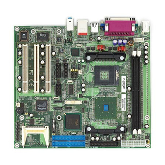
Page 19: Board Layout
Board Layout (Optional) DIMM1 DIMM2 CN13 CN14 CN15 CN25 CN10 CN12 CN11 CN16 CN17 CN18 SATA1 CN19 SATA2 CF II CN21 CN22 CN24 CN20 CN23 Figure 8: Jumper and Connector Locations Installation • 13... -
Page 20: Jumper Settings
Jumper Settings Jumper Location Description: Use the information in the following table to change the jumpers and the DIP switches. Jumpers Functions COM3 Port Setting Select COM4 Port Setting Select CPU Type Setting Select Watchdog Timer Setting Select Clear CMOS Setting Select Power Management Setting Select A description on setting the jumpers to enable/disable or change functions is illustrated below. - Page 21 CPU Type Setting Select: JP3 Function CPU FSB 400 MHz (Default) 1-2 On CPU FSB 533 MHz 1-2 Off Location: Watchdog Timer Setting Select: JP4 Function Reset System (Default) Location: Clear CMOS Setting Select: JP5 Function Normal (Default) Clear CMOS Location: Installation •...
-
Page 22: Connector Descriptions
Power Management Setting Select: JP6 Function ACPI Mode APM Mode (Default) Location: Connector Descriptions (Optional) DIMM1 DIMM2 CN14 CN13 CN15 CN25 CN10 CN12 CN11 CN16 CN17 CN18 SATA1 CN19 SATA2 CF II CN21 CN22 CN24 CN20 CN23 Figure 9: Connector Locations 16 •... - Page 23 Table for Connector’s Location Description: Use the information in the following table to change the connector. Connectors Functions CRT VGA Port Connector COM1 RS-232 Serial Port Connector Parallel Port Connector USB 0/1 Connectors Audio Port Connector (Optional) PS/2 Keyboard & Mouse Connectors Gigabit Ethernet RJ-45 &...
- Page 24 CRT VGA Port Connector (D-SUB 15-pins Female): CN1 Pin # Assignment Pin # Assignment Green Blue Ground Ground Ground Ground Ground DData HSync VSync Figure: COM1 RS-232 Serial Port Connector (D-Sub 9-pins Male): CN2 Pin # Assignment Pin # Assignment DCD (Data Carrier Detect) DSR (Data Set Ready) RXD (Receive Data)
- Page 25 Parallel Port Connector (D-Sub 25-pins Male): CN3 Pin # Assignment Pin # Assignment Line Printer Strobe Auto Feed PD 0, Parallel Data 0 Error PD 1, Parallel Data 1 Initialize PD 2, Parallel Data 2 Select PD 3, Parallel Data 3 Ground PD 4, Parallel Data 4 Ground...
- Page 26 Audio Port Connector (Audio Phone–Jack): CN5 (Optional) Pin # Assignment BLUE Line-In GREEN Line-Out Mic-In Figure: Blue Green PS/2 Keyboard Connector (6-pins Green Mini Din): CN6 Pin # Assignment Pin # Assignment Keyboard Data Ground Keyboard Clock Figure: PS/2 Mouse Connector (6-pins Purple Mini Din): CN6 Pin # Assignment Pin #...
- Page 27 Gigabit Ethernet RJ-45 Connector (RJ-45 Phone–Jack): CN7 Pin # Assignment Pin # Assignment Transmit output (+) Transmit output (-) Receive input (-) Receive input (+) Figure: USB 2/3 Connector (4-pins Female): CN7 Pin # Assignment Pin # Assignment USB2 - USB3 - USB2 + USB3 +...
- Page 28 CD_IN Connector: CN9 Pin # Assignment CD_IN_Left CD_GND CD_GND CD_IN_Right Figure: COM3 RS-232/422/485 Serial Port Connectors (14-pins Pin-Header): CN13 Pin # Assignment Pin # Assignment Ground Ground TXD+ TXD- RXD+ RXD- COM3 Figure: 22 • Installation...
- Page 29 COM4 RS-232/422/485 Serial Port Connectors (14-pins Pin-Header): CN14 Pin # Assignment Pin # Assignment Ground Ground TXD+ TXD- RXD+ RXD- COM4 Figure: Note: How to connect a RS485 device with the COM port ribbon cable? Our Industrial Board encloses a COM port ribbon cable for internal connection. RS422/485 device must connect to downside D-Sub with 5-pin cable and signal indication as below.
- Page 30 CPU Fan Power Connector: CN15 Pin # Assignment Ground Fan Status Signal Figure: COM2 RS-232 Serial Port Connector (10-pins Pin-Header): CN16 Pin # Assignment Pin # Assignment Ground Ground Figure: 18/24 Bits LVDS Panel Interface (40-pins Male): CN17 Pin # Assignment Pin # Assignment...
- Page 31 Ground Ground YBM1 YBM2 YBP1 YBP2 Ground Ground CLKBM YBM3 CLKBP YBP3 +12V +12V PVCC PVCC Figure: System Fan Power Connector: CN18 Pin # Assignment Ground Fan Status Signal Figure: Installation • 25...
- Page 32 USB 4/5 Connector (9-pins Pin-Header): CN19 Pin # Assignment Pin # Assignment USB4 - USB5 - USB4 + USB5 + Ground Ground Figure: System Panel Indicate Connector: CN20 Pin # Assignment Pin # Assignment SPEAKER PWR LED PWLED+ BUZZER PWLED- KEYLOCK SPEAKER HDD LED...
- Page 33 Secondary IDE Connector (40-pins 2.54mm Pitch Pin-Header with Housing): CN21 Pin # Assignment Pin # Assignment Reset IDE Ground Host Data 7 Host Data 8 Host Data 6 Host Data 9 Host Data 5 Host Data 10 Host Data 4 Host Data 11 Host Data 3 Host Data 12...
- Page 34 ATX Power Connector: CN22 Pin # Assignment Pin # Assignment +3.3V +3.3V +3.3V -12V Ground Ground PS-ON Ground Ground Ground Ground Ground 5VSB +12v Figure: Primary IDE Connector (40-pins 2.54mm Pitch Pin-Header with Housing): CN23 Pin # Assignment Pin # Assignment Reset IDE Ground...
- Page 35 Address 0 Address 2 Chip Select 0 Chip Select 1 Activity Ground Figure: Floppy Disk Connector (34-pins 2.54mm Pitch Pin-Header with Housing): CN24 Pin # Assignment Pin # Assignment Ground Drive Density Selection Ground Ground Drive Density Selection Ground Index Ground Motor Enable 0 Ground...
- Page 36 LINE OUT Connector: CN25 Pin # Assignment LOUT_L AU_GND VCC_5V LOUT_R Figure: LAN LED Connector: JP7 Pin # Assignment Pin # Assignment LINK_LED VCC_3V ACT_LED VCC_3V Figure: 30 • Installation...
- Page 37 S-ATA1 Connector (9-pins): SATA1 Pin # Assignment Ground SATA1_TXP SATA1_TXN Ground SATA1_RXN SATA1_RXP Ground Ground Ground Figure: S-ATA2 Connector (9-pins): SATA2 Pin # Assignment Ground SATA2_TXP SATA2_TXN Ground SATA2_RXN SATA2_RXP Ground Ground Ground Figure: Installation • 31...
- Page 38 Type II CompactFlash™ Connector: CF II Pin # Assignment Pin # Assignment Ground CS#1 Ground Ground Ground Ground Ground Ground Ground Ground Ground CS#3 IOR# IOW# INTS CSEL# IDERST# IORDY IDEACTS# Ground Ground Ground Figure: 32 • Installation...
-
Page 39: Chapter 3 Award Bios Setup
Award BIOS Setup BIOS Instructions Award’s ROM BIOS provides a built-in Setup program, which allows the user to modify the basic system configuration and hardware parameters. The modified data will be stored in a battery-backed CMOS, so that data will be retained even when the power is turned off. - Page 40 Phoenix - AwardBIOS CMOS Setup Utility Standard CMOS Feature Frequency/Voltage Control Advanced BIOS Feature Load Fail-Safe Defaults Advanced Chipset Feature Load Optimized Defaults Integrated Peripherals Set Supervisor Password Power Management Setup Set User Password PnP/PCI Configurations Save & Exit Setup PC Health Status Exit Without Saving ↑...
-
Page 41: Standard Cmos Features
Use this menu to show your system temperature, speed and voltage status. See 3.10 for the details. Frequency / Voltage Control: Use this menu to specify your settings for frequency/voltage control. See 3.11 for the details. Load Fail-Safe Defaults: Use this menu to load the BIOS default values for the minimal/stable performance for your system to operate. - Page 42 Standard CMOS Features Date (mm:dd:yy): Mon, JUN 7 2004 Item Help Time (hh:mm:ss): 16:19:20 ____________________________ IDE Primary Master 13579 MB Menu Level IDE Primary Slave None IDE Secondary Master None Change the day, month, year and IDE Secondary Slave None century Drive A 1.44M, 3.5 in.
-
Page 43: Ide Adapters
Video: Options EGA/VGA/CGA 40/CGA 80/MONO Select the default video device. Halt On: Options All Errors/No Errors/All, All but Keyboard/All, All but Diskette/All, All but Disk/Key Select the situation in which you want the BIOS to stop the POST process and notify you. - Page 44 IDE Primary Master: Options None, Auto and Manual Selecting “Manual” lets you set the remaining fields on this screen. Selects the type of fixed disk. "User Type" will let you select the number of cylinders, heads, etc. Note: PRECOMP=65535 means NONE! Access Mode: Options CHS, LBA, Large and Auto Choose the access mode for this hard disk Capacity: Options Auto Display your disk drive size...
-
Page 45: Advanced Bios Features
3.5 Advanced BIOS Features This section allows you to configure your system for basic operation. You have the opportunity to select the system’s default speed, boot-up sequence, keyboard operation, shadowing and security. Phoenix - AwardBIOS CMOS Setup Utility Advanced BIOS Features CPU Feature Press Enter Item Help... - Page 46 Hard Disk Boot Priority: Press Enter and It shows Bootable add-in Card. Virus Warning: Allow you to choose the VIRUS Warning feature for IDE Hard Disk boot sector protection. If this function is enabled and someone attempts to write data into this area, BIOS will show a warning message on screen and alarm beep.
- Page 47 Boot Up Floppy Seek: Seeks disk drives during boot up. Disabling speeds boot up. The choices: Enabled, Disabled. Boot Up NumLock Status: Select power on state for NumLock. The choices: On, Off Gate A20 Option: Select if chipset or keyboard controller should control GateA20. Normal---A pin in the keyboard controller controls GateA20 Fast---Lets chipset control GateA20 Typematic Rate Setting:...
-
Page 48: Advanced Chipset Features
Select the operating system that is running with greater than 64MB of RAM on the system. The choices: Non-OS2, OS2. Report No FDD For Win 95: Whether report no FDD for Windows 95 or not. The choices: Yes, No. 3.6 Advanced Chipset Features This section allows you to configure the system based on the specific features of the installed chipset. - Page 49 Select the operating system that is selecting DRAM timing, so select SPD for setting SDRAM timing by SPD. The choices: Manual, By SPD. CAS Latency Time: When synchronous DRAM is installed, the number of clock cycles of CAS latency depends on the DRAM timing. The choices: 2, 2.5.
- Page 50 The choices: Enabled, Disabled. Video BIOS Cacheable: Select “Enabled” allows caching of the video BIOS, resulting in better system performance. However, if any program writes to this memory area, a system error may result. The choices: Enabled, Disabled. Memory Hole At 15M-16M: You can reserve this area of system memory for ISA adapter ROM.
-
Page 51: Integrated Peripherals
The choices: VBIOS Default, CRT, LFP and CRT+LEP. Panel Number: This item allows you to select the panel resolution. The choices: 1-8. 3.7 Integrated Peripherals Phoenix - AwardBIOS CMOS Setup Utility Integrated Peripherals Onboard IDE Device Press Enter Item Help Onboard Device Press Enter ____________________________... - Page 52 OnChip Primary/Secondary PCI IDE: The integrated peripheral controller contains an IDE interface with support for two IDE channels. Select “Enabled” to activate each channel separately. The choices: Enabled, Disabled. IDE Primary/Secondary Master/Slave PIO: The four IDE PIO (Programmed Input/Output) fields let you set a PIO mode (0-4) for each of the four IDE devices that the onboard IDE interface supports.
- Page 53 USB Keyboard Support: Select “Enabled” if your system contains a Universal Serial Bus (USB) controller and you have a USB keyboard. The choices: Enabled, Disabled. USB Mouse Support: Select “Enabled” if your system contains a Universal Serial Bus (USB) controller and you have a USB mouse.
- Page 54 KB Power ON Password: You can use this item to limit operating KB Power On system. The choice: Enter Hot Key Power ON: You can use this item to select operating Hot Key to Power On system. The choices: Ctrl-F1~Ctrl-F12. Onboard FDC Controller: Select “Enabled”...
-
Page 55: Power Management Setup
Onboard Serial Port 1/Port 2: Select an address for the first and second serial ports. Serial Port 1/Port 2 Use IRQ: Select an IRQ for the first and second serial ports. Onboard Serial Port 3/Port 4: Select an address for the third and forth serial ports. Serial Port 3/Port 4 Use IRQ: Select an IRQ for the third and forth serial ports. - Page 56 This item allows you to enable or disable the Advanced Configuration and Power Management (ACI). The choices: Enabled, Disabled. Power Management: This category allows you to select the type (or degree) of power saving and is directly related to the following modes: 1.
- Page 57 Suspend Type: Select the Suspend Type. The choices: PWRON Suspend, Stop Grant. Suspend Mode: When “Enabled” and after the set time of system inactivity. All devices except the CPU will be shut off. The choices: Enabled, Disabled. HDD Power Down: When “Enabled”...
-
Page 58: Pnp/Pci Configurations
3.9 PnP/PCI Configurations This section describes configuring the PCI bus system. PCI, or Personal Computer Interconnect, is a system that allows I/O devices to operate at speeds nearing the speed the CPU itself uses when communicating with its own special components. This section covers some very technical items and it is strongly recommended that only experienced users should make any changes to the default settings. -
Page 59: Pc Health Status
3.10 PC Health Status Phoenix - AwardBIOS CMOS Setup Utility PC Health Status CPU Warning Temperature Disabled Item Help Temperature 32°C / 89°F ____________________________ Temperature 28°C / 82°F CPU FAN 5152RPM Menu Level SYSFAN 3283RPM VDIMM 2.48 VCORE 4.42V +3.3 3.34V + 5 V 4.94V... -
Page 60: Frequency/Voltage Control
+3.3V/+5V/+12V/-12V/-5V/5VSB(V): Displays the voltage of +5V/+12V/-12V/-5V. VBAT (V): Displays the voltage level of the battery. Shutdown Temperature: This item allows you to set up the CPU shutdown Temperature. This item is only ® effective under Windows 98 ACPI mode. The choices: Disabled, 60°C / 140°F, 65°C / 149°F, 70°C / 159°F and 75°C / 167°F. -
Page 61: Load Optimized Defaults
Load Fail-Safe Defaults (Y/N)? N Pressing ‘Y’ loads the BIOS default values for the most stable, minimal-performance system operations. 3.13 Load Optimized Defaults When you press <Enter> on this item you get a confirmation dialog box with a message similar to: Load Optimized Defaults (Y/N)? N Pressing ‘Y’... -
Page 62: Exiting Bios Setup
PASSWORD DISABLED. When a password has been enabled, you will be prompted to enter it every time you try to enter Setup. This prevents an unauthorized person from changing any part of your system configuration. Additionally, when a password is enabled, you can also require the BIOS to request a password every time your system is rebooted. -
Page 63: Warranty Policy
Warranty Policy Thank you for choosing ADLINK. To understand your rights and enjoy all the after-sales services we offer, please read the following carefully. Before using ADLINK’s products please read the user manual and follow the instructions exactly. When sending in damaged products for repair, please attach an RMA application form which can be downloaded from: http://rma.adlinktech.com/policy/.
Need help?
Do you have a question about the M-855 Series and is the answer not in the manual?
Questions and answers