
Related Manuals for ADLINK Technology M-302


Summary of Contents for ADLINK Technology M-302
- Page 1 M-302 ATX Industrial Motherboard with Intel® Q965 Chipset User’s Manual Manual Rev.: 2.01 Revision Date: July 30, 2012 Part No: 50-13062-1010 Advance Technologies; Automate the World.
- Page 2 Revision History Revision Release Date Description of Change(s) 2.00 2009/09/08 Initial Release Correct CPU Fan Connector pin definition; remove CHA_FAN1; add WDT sample code; 2.01 2012/07/30 update audio codec for boards with ordering numbers ending in “0070” and higher; update CPU support.
-
Page 3: Preface
M-302 Preface Copyright 2009-12 ADLINK Technology Inc. This document contains proprietary information protected by copy- right. All rights are reserved. No part of this manual may be repro- duced by any mechanical, electronic, or other means in any form without prior written permission of the manufacturer. - Page 4 Using this Manual Audience and Scope The M-302 User’s Manual is intended for hardware technicians and systems operators with knowledge of installing, configuring and operating industrial grade computers. Manual Organization This manual is organized as follows: Preface: Presents copyright notifications, disclaimers, trade- marks, and associated information on the proper usage of this document and its associated product(s).
- Page 5 M-302 Conventions Take note of the following conventions used throughout this manual to make sure that users perform certain tasks and instructions properly. Additional information, aids, and tips that help users perform tasks. NOTE: NOTE: Information to prevent minor physical injury, component dam- age, data loss, and/or program corruption when trying to com- plete a task.
- Page 6 This page intentionally left blank. Preface...
-
Page 7: Table Of Contents
M-302 Table of Contents Revision History..............ii Preface ..................iii List of Figures ................ ix List of Tables................xi 1 Introduction ................ 1 Package Contents ............... 1 Overview................2 Features................2 Specifications............... 3 Power Consumption ............5 Block Diagram ..............7 Functional Description ............ - Page 8 Advanced BIOS Features ..........43 Advanced Chipset Features..........48 Integrated Peripherals............50 Power Management Setup ..........55 PnP/PCI Configurations ............. 58 Frequency/Voltage Control ..........60 Load Fail-Safe Defaults ............. 61 4.10 Load Optimized Defaults............ 62 4.11 Set Supervisor & User Password........63 4.12 Save &...
-
Page 9: List Of Figures
M-302 List of Figures Figure 1-1: M-302 Block Diagram ............7 Figure 1-2: M-302 Board Layout ............11 Figure 1-3: M-302 Rear I/O Layout ..........12 Figure 1-4: M-302 Board Dimensions ..........13 List of Figures... - Page 10 This page intentionally left blank. List of Figures...
-
Page 11: List Of Tables
Table 1-1: M-302 General Specifications.......... 4 Table 1-2: Pentium® 4 651 Power Consumption ......5 Table 1-3: Core™2 Duo E6400 Power Consumption ....... 6 Table 1-4: M-302 Board Layout Legend ......... 12 Table B-1: System Memory Map............. 75 Table B-2: Direct Memory Access Channels........76 Table B-3: Fixed I/O Map .............. - Page 12 This page intentionally left blank. List of Tables...
-
Page 13: Introduction
M-302 Introduction This chapter will introduce the M-302, its features, specifications, functional description, and mechanical layout. 1.1 Package Contents Please check that your package contains the items below. If you discover damaged or missing items, please contact your vendor. M-302 Industrial ATX Motherboard... -
Page 14: Overview
LGA775 package to deliver a high-performance, full-fea- tured motherboard for a wide array of embedded computing appli- cations. The M-302 supports a broad range of processing speeds, complete I/O functions, and high-bandwidth network connectivity . These advanced features, coupled with a dual-channel DDR2 sys-... -
Page 15: Specifications
M-302 1.4 Specifications System CPU/Cache • Intel® Core™2 Duo Processor E7400*, 45nm, 3 MB L2, 2.8 GHz, 1066 MHz • Intel® Core™2 Duo Processor E6400, 65nm, 2 MB L2, 2.13 GHz, 1066 MHz • Intel® Core™2 Duo Processor E4300, 65nm, 2 MB L2, 1.8 GHz, 800 MHz •... -
Page 16: Table 1-1: M-302 General Specifications
Dimensions • 305 x 244 mm (L x W) Operating • 0°C to 60°C Temp. Storage • -20ºC to 80ºC Temp. Rel. • 10 - 90% RH Humidity Safety • CE, FCC Class A Table 1-1: M-302 General Specifications Introduction... -
Page 17: Power Consumption
M-302 Power Consumption Intel® Pentium® 4 processor 651, 65nm, SL9KE, 2MB L2, 3.40GHz, FSB 800MHz Test Configuration Memory Transcend 2G DDR2-800 DIMM Graphics 82Q963/965 Integrated Graphics Controller IDE Channel Seagate Barracuda 7200.7 80G ST380013A Power Supply ZIPPY P1G-6250P 250W Power Req. -
Page 18: Table 1-3: Core™2 Duo E6400 Power Consumption
Intel® Core™2 Duo processor E6400, 65nm, SL9T9, 2MB L2, 2.13GHz, FSB 1066MHz Test Configuration Memory Transcend 2G DDR2-800 DIMM Graphics 82Q963/965 Integrated Graphics Controller IDE Channel Seagate Barracuda 7200.7 80G ST380013A Power Supply ZIPPY P1G-6250P 250W Power Req. +3.3V +12V Total Current (A) 2.488... -
Page 19: Block Diagram
Audio COM 3 Fintek F81216 LPC to UART COM 4 HD Audio Audio Jacks Codec Header for 16Mbit SPI BIOS Printer Port KB/Mouse Winbond W83627DHG Hardware COM 1 LPC Super I/O Monitor COM 2 Figure 1-1: M-302 Block Diagram Introduction... -
Page 20: Functional Description
533/800/1066 MHz Front Side Bus (FSB). Providing high-performance computing and energy-efficiency, the M-302 is designed for Intel® Core™2 Duo, Intel® Pentium® Dual- Core, Intel® Pentium® 4, Intel® Celeron®, and Intel® Celeron® D processors. The M-302 supports dual-core processors containing multiple physical cores and dedicated L2 caches to meet the ever- increasing demands of industrial computing. - Page 21 Serial ATA Storage is efficient and secure with the Serial ATA interface. Utiliz- ing the Intel® ICH8DO, the M-302 supports up to six Serial ATA devices capable of reading/writing data at up to 3 Gbps. The SATA specification improves chassis airflow via thinner and more flexible cables with lower pin count.
- Page 22 Watchdog Timer The watchdog timer (WDT) monitors system operations based on user-defined configurations. The WDT can be programmed for dif- ferent time-out periods, such as from 1 to 255 seconds or from 1 to 255 minutes. The WDT generates a reset signal, then a reset request, after failure to strobe it within the programmed time period.
-
Page 23: Board Layout
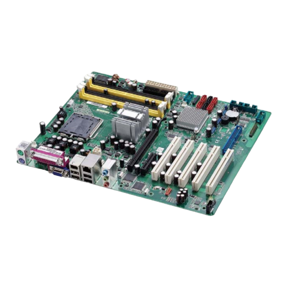
PWR_FAN CPU_FAN KBPWR ATX12V FLOPPY EATXPWR LAN_LED_HD PCIEX16 CHA_FAN2 PCIEX4_1 COM1 TPM_SLOT PCI1 SATA1/2 SATA5/6 JSPI PCI2 SATA3/4 IE1394_2 USB56 USB78 USB910 PCI3 CLRTC COM3 PCI4 PRI_IDE IR_CON1 COM2 PCI5 AAFP F_PANEL1 COM4 SPDIF_OUT Figure 1-2: M-302 Board Layout Introduction... -
Page 24: Figure 1-3: M-302 Rear I/O Layout
Floppy connector SPDIF_OUT SPDIF pin header IE1394_2 IEEE 1394a pin header TPM_SLOT TPM connector IR_CON1 IrDA pin header USB5-10 USB pin headers Table 1-4: M-302 Board Layout Legend Audio Parallel Port 1394A USB1/2 USB3/4 Figure 1-3: M-302 Rear I/O Layout Introduction... -
Page 25: Mechanical Drawing
M-302 1.9 Mechanical Drawing Dimensions in mm Figure 1-4: M-302 Board Dimensions Introduction... - Page 26 This page intentionally left blank. Introduction...
-
Page 27: Connectors & Jumpers
M-302 Connectors & Jumpers The connectors and jumpers on the M-302 allow you to connect and configure external devices. The following specify the pin assignments for connectors and jumper on the M-302. Refer to Figure 1-2: M-302 Board Layout and Figure 1-3: M-302 Rear I/O Layout for connector and jumper locations. - Page 28 VGA Connector. Signal Name Pin # Pin # Signal Name Green Blue VCC pull-up VCC pull-up DDC2B DATA HSYNC VSYNC DDC2B CLK Parallel Port. Pin # Signal Name Pin # Signal Name STROBE AUTO FEED DATA0 ERROR DATA1 INIT DATA2 SELECT IN DATA3 DATA4...
- Page 29 M-302 USB Connectors Pin # Signal Name USB- USB+ LAN Port (RJ-45) This port allows gigabit connection to a Local Area Network (LAN) using a network hub. The LAN port comes with two LEDs to indi- cate link, activity and speed. Refer to the tables below for the LAN port pin and LED definitions .
- Page 30 IEEE 1394a Port Pin # Signal Name +12V Audio I/O port The three-jack audio I/O supports Line-In, Line-Out, and Mic-In functions. The blue Line-In jack onnects to an audio source such as a CD player. The green Line-Out port connects to a speaker or headphone, while the pink Mic-In jack connects to a microphone.
-
Page 31: Onboard Connectors
M-302 2.2 Onboard Connectors Front Panel Audio Pin Header (AAFP) Pin # Signal MIC2_L MIC2_R FP_PRES# LIN2_R SRTN1 SENSE A LIN2_L SRTN2 ATX 12V Power Connector (ATX12V) Pin # Signal +12V DC +12V DC CD-in Connector (CD) Pin # Signal... - Page 32 System Fan Connector (CHA_FAN2) Pin # Signal Fan Power (+12V) Fan Tachometer Serial Port Connectors (COM1-4) Pin # Signal Functions Data Carrier Detect Transmit Data Ground Request to Send Ring Indicate Receive Data Data Terminal Ready Data Set Ready Clear to Send Not Connect CPU Fan Connector (CPU_FAN) Pin #...
- Page 33 M-302 ATX Power Connector (EATXPWR) Pin # Signal Pin # Signal +3.3V +3.3V +3.3V -12V PS-ON# PWRGD +5VSB +12V +12V 24-pin detection Connectors & Jumpers...
- Page 34 System Panel Connector (F_PANEL1) Pin # Signal Function Pin Group Power for +5v Power LED HC_PLED-L Power LED signal Ground Ground Reserved ATX_PSON-L ATX Power-on signal Power for +5v P5V_SB_ATX Standby HC_SPKR Speaker signal Chassis Speaker Power for +5v HC_RSTBN-L RESET signal Reset Button Ground...
- Page 35 M-302 Floppy disk drive connector (FLOPPY) Pin # Signal Pin # Signal Extended Density No Connect Data Rate Index Motor A Select Drive B Select Drive A Select Motor B Select Step Direction Step Pulse Write Data Write Gate Track 0...
- Page 36 IrDA Pin Header (IR_CON1) Pin # Signal IRRX IRTX LAN LED Pin Header (LAN_LED_HD) Pin # Signal ACTLEDP NIN_ACTLED# NIN_LINKLED1# R_NIN_LINKLED2# R_NIN_LINKLED2# NIN_LINKLED1# Connectors & Jumpers...
- Page 37 M-302 IDE Connector (PRI_IDE) Pin # Signal Pin # Signal Reset Ground Data 7 Data 8 Data 6 Data 9 Data 5 Data 10 Data 4 Data 11 Data 3 Data 12 Data 2 Data 13 Data 1 Data 14...
- Page 38 SATA Connectors (SATA1-6) Pin # Signal SPDIF Pin Header (SPDIF_OUT) Pin # Signal SPDIF0 Connectors & Jumpers...
- Page 39 M-302 TPM Connector (TPM_SLOT) Pin # Signal CK-LPC_TPM LFRAME# SMBDATA_DDR PLTRST# SMBCLK_DDR LAD3 LAD2 LAD1 LAD0 +3VSB SERIRQ CLKRUN# LPCPD# USB 2.0 Connector (USB5-10) Pin # Signal Pin # Signal USB0- USB1- USB0+ USB01+ Connectors & Jumpers...
-
Page 40: Jumpers
The CMOS RAM data contains the date / time and BIOS setting information. CMOS is powered by the onboard button cell battery. To erase the CMOS RAM data: 1. Unplug the M-302 2. Short the CLRTC pins 2-3 3. Turn the power on. After power on, remove the jumper cap from pins 2-3 and reinstall it to pins 1-2. -
Page 41: Getting Started
M-302 Getting Started This chapter provides information on how to install components to the M-302 SBC. Specifically, the installation of CPU, memory mod- ules, and operating system are explained. 3.1 Installing the CPU The M-302 Supports the Intel® Core™2 Duo, Intel® Pentium®... - Page 42 2. Lift and rotate the load lever to a 135° angle 3. Lift the load plate to a 100° angle using your thumb and forefinger 4. Use your thumb to push and remove the protective socket cover (plastic) from the load plate Getting Started...
- Page 43 M-302 5. Position the CPU over the socket, then match the notches on the CPU side with the alignment keys on the socket. The golden triangle on the CPU must be posi- tioned on the bottom-left corner of the socket .
- Page 44 7. Close the load plate (A), then fasten the load lever on the retention tab (B) . Getting Started...
-
Page 45: System Memory
M-302 3.2 System Memory The M-302 supports up to 8 GB of DDR2 533/667/800 SDRAM in four 240-pin DIMM sockets. See Figure 1-2 on page 11 for DIMM socket locations. Memory Configurations Dual channel configuration is supported by the M-302 as follows:... - Page 46 To install a memory module: 1. Locate the DIMM slots on the motherboard. 2. Press the socket’s retaining clips outward to unlock. 3. Align the memory module on the socket making sure that the notch matches the break on the socket. Notch Break 4.
-
Page 47: Driver Installation
M-302 3.3 Driver Installation The M-302 drivers for Windows XP 32-bit are located in the fol- lowing directories on the Driver DVD, or can be downloaded from the ADLINK website (http://www.adlinktech.com): Chipset X:\M-302 Driver\INF Display X:\M-302 Driver\VGA\WIN2KXP_32 X:\M-302 Driver\LAN\Windows\2000_ XP_2003 Server... - Page 48 This page intentionally left blank. Getting Started...
-
Page 49: Bios Setup
M-302 BIOS Setup The following chapter describes basic navigation for the Phoenix AwardBIOS Setup Utility. 4.1 Starting the BIOS To enter the setup screen, follow these steps: 1. Power on the motherboard 2. Press the <Delete> key on your keyboard during the Power-On-Self-Test (POST) to enter the Setup utility. - Page 50 Navigation Use the keys described below to navigate through the BIOS Setup Utility Key(s) Function Description General help, only for Status Page Setup Menu and Option Page Setup Menu Return to the main menu from a sub-menu or prompts you to quit the setup program. ←...
-
Page 51: Standard Cmos Features
M-302 4.2 Standard CMOS Features The main menu includes the following setup categories. Recall that some systems may not include all entries. Date/Time Use this option to change the system time and date. The date must be entered in MM/DD/YY format. The time is entered in HH:MM:SS format. - Page 52 IDE HDD Auto-detection: Press Enter Press Enter to auto-detect the HDD on the selected channel. IDE Device Setup: None/Auto/Manual Selecting 'manual' allows the user to set the remaining fields on the submenu. Selects the type of fixed disk. "User Type" will let you select the number of cyl- inders, heads, etc.
- Page 53 M-302 Drive A Specifies the capacity and physic al size of diskette drive A. Do not select [None] if you are using a floppy disk drive. Configuration options: [None] [360K, 5.25 in.] [1.2M , 5.25 in.] [720K , 3.5 in.] [1.44M, 3.5 in.] [2.88M, 3.5 in.]...
- Page 54 Halt On During the Power On Self Test (POST), the computer stops if the BIOS detects a hardware error. The BIOS can be instructed to ignore certain errors during POST and continue the bootup pro- cess. The options are as follows: No errors: POST does not stop for any errors.
-
Page 55: Advanced Bios Features
M-302 4.3 Advanced BIOS Features This section allows users to configure the Advanced BIOS Fea- tures of the system. BIOS Setup... - Page 56 CPU Features Thermal Management Options: Thermal Monitor 1 and Thermal Monitor 2. PPM Mode Options: Native Mode/SMM Mode Limit CPUID MaxVal Set Limit CPUID MaxVal to 3. This should be disabled for WinXP C1E Function CPU C1E function select Execute Disable Bit When disabled, forces the XD feature flag to always return 0 Hard Disk Boot Priority Sets hard disk boot device priority.
- Page 57 M-302 Virus Warning Enables or disables the virus warning. CPU L1 & L2 Cache Enables or disables the CPU L1 & L2 Cache. Enabling this feature speeds up memory access. Hyper-Threading Technology Enables or disables the Hyper-Threading function of the CPU.
- Page 58 Typematic Rate (Chars/Sec.) Sets number of characters that can be typed per second on the keyboard. Typematic Delay (Msec) The time (in milliseconds) needed before accepting a subsequent keystroke on the keyboard. Security Option Selects whether a password is required every time the system boots or only when setup is entered.
- Page 59 M-302 Console Redirection Enables/Disables the remote Console Function. Baud Rate When Console Redirection is Enabled, the BIOS will allow users to set the serial port's operating baud rate. Options: 9600 bps, 19200 bps, 38400 bps, 57600 bps, and 115200 bps.
-
Page 60: Advanced Chipset Features
4.4 Advanced Chipset Features System BIOS Cacheable Selecting “Enabled” allows caching of the system BIOS ROM at F0000h- FFFFFh, resulting in better system performance. How- ever, if any program writes data to this memory area, a system error may occur. The options are “Enabled”, and “Disabled”. Memory Hole at 15M-16M Enabling this feature reserves 15 MB to 16 MB memory address space for ISA expansion cards that specifically require this setting. - Page 61 M-302 VGA Settings PEG/Onchip VGA Control The options are “Auto”, “Onchip VGA” or “PEG Port”. On-Chip Frame Buffer Size The On-Chip Frame Buffer Size can be set to 1 MB or 8 MB. This memory is shared with the system memory.
-
Page 62: Integrated Peripherals
4.5 Integrated Peripherals On Chip IDE Device BIOS Setup... - Page 63 M-302 IDE HDD Block Mode If your IDE hard drive supports block mode select Enabled for automatic detection of the optimal number of block read/writes per sector the drive can support. IDE DMA Transfer Access Use this field to enable or disable IDE DMA transfer access.
- Page 64 Super I/O Device Power ON Function This feature allows you to wake up the system using any of the listed options. The selections are “Hot KEY”, “Mouse Left”, “Mouse Right”, “Any KEY” and “BUTTON ONLY”. Hot Key Power ON Awaken the system by pressing the hot key button. The options are “Ctrl-F1”, “Ctrl-F2”, “Ctrl-F3”...
- Page 65 M-302 Onboard Parallel Port This field sets the address of the on-board parallel port connector. You can select “378/IRQ7”, “278/IRQ5”, “3BC/IRQ7”, or “Dis- abled”. If you install an I/O card with a parallel port, make sure there is no conflict in the address assignments. The single board computer can support up to three parallel ports.
- Page 66 USB Device Setting USB 1.0 / 2.0 Controller The options: Disabled, Enabled. USB Operation Mode Allows you to configure the USB 2.0 controller in HiSpeed (480 Mbps) or Full Speed (12 Mbps). Configuration options: [Full/Low Speed] [HiSpeed] USB Keyboard Function The options: Disabled, Enabled.
-
Page 67: Power Management Setup
M-302 4.6 Power Management Setup PCI Express PM Function This option enables/disables system wake up by PCI Express device. ACPI Function The options are “Enabled” and “Disabled”. ACPI Suspend Type This item allows you to set ACPI suspend type to S1/POS (Power On Suspend) or S3/STR (Suspend To RAM). - Page 68 Max. Power Saving: Maximum power management, HDD Power Down =1 Min User Defined: Allows you to set each mode individually. When not disabled, each of the ranges are from 1 min. to 1 hr. except for HDD Power Down which ranges from 1 min. to 15 min.
- Page 69 M-302 Power On by Ring Select “Enabled” to power on the system from a soft off state by an input signal on the serial Ring Indicator (RI) line. The options are “Enabled” and “Disabled”. USB KB Wake-Up from S3 When “Enabled”, enter any key to wake up the system from S3 state.
-
Page 70: Pnp/Pci Configurations
4.7 PnP/PCI Configurations This section describes configuring the PCI (Personal Computer Interconnect) bus system. PCI is a system which allows I/O devices to operate at speeds nearing the speed the CPU itself uses when communicating with its own components. Init Display First This item allows you to choose the first display interface to initiate while booting. - Page 71 M-302 PCI/VGA Palette Snoop PCI Latency Timer (CLK). Min = 0 , Max = 225 INT Pin 1/2/3/4/5/6/7/8 Assignment The options: Auto, 3, 4, 5, 7, 9, 10, 11 Maximum Payload Size This allows you to set the maximum TLP payload size for PCI Express devices.
-
Page 72: Frequency/Voltage Control
4.8 Frequency/Voltage Control Spread Spectrum This setting allows you to reduce EMI by modulating the signals the CPU generates so that the spikes are reduced to flatter curves. This is achieved by varying the frequency slightly so that the signal does not use any particular frequency for more than a moment. -
Page 73: Load Fail-Safe Defaults
M-302 4.9 Load Fail-Safe Defaults Use this menu to load the BIOS default values for the minimal/sta- ble performance for your system to operate. Press <Y> to load the BIOS default values for the most stable, minimal-performance sys- tem operations. -
Page 74: Load Optimized Defaults
4.10 Load Optimized Defaults Use this menu to load the BIOS default values that are factory set- tings for optimal performance system operations. While Award has designed the custom BIOS to maximize performance, the factory can change these defaults to meet its needs. Press <Y> to load the default values setting for optimal performance system opera- tions. -
Page 75: Set Supervisor & User Password
M-302 4.11 Set Supervisor & User Password These two options set the system password. Supervisor Password sets a password that will be used to protect the system and Setup utility. User Password sets a password that will be used exclu- sively on the system. -
Page 76: Save & Exit Setup
4.12 Save & Exit Setup This option allows you to determine whether to accept any modifi- cations or not. Typing Y will quit the setup utility and save all changes into the CMOS memory. Typing N will return to the Setup Utility Main Screen. -
Page 77: Exit Without Saving
M-302 4.13 Exit Without Saving Select this option to exit the Setup utility without saving the changes you have made in this session. Typing Y will quit the Setup utility without saving any modifications. Typing N will return to Setup utility. - Page 78 This page intentionally left blank. BIOS Setup...
-
Page 79: Post Codes
M-302 POST Codes The following is a list of M-302 POST Codes. Code (hex) Description Test CMOS read/write functionality Early chipset initialization: Disable shadow RAM, L2 cache (socket 7 and below), program basic chipset registers Detect memory: Auto detection of DRAM size, type and ECC, auto... - Page 80 Code (hex) Description Reserved Program chipset default values into chipset. Chipset default values are MODBINable by OEM customers Reserved Initial Early_Init_Onboard_Generator switch Reserved Detect CPU information including brand, SMI type (Cyrix or Intel) and CPU level (586 or 686) Reserved Reserved Initial interrupts vector table.
- Page 81 M-302 Code (hex) Description Program CPU internal MTRR (P6 & PII) for 0-640K memory address; Initialize the APIC for Pentium class CPU; Program early chipset according to CMOS setup; Measure CPU speed; Invoke video BIOS Reserved Reserved Reserved Initialize multilanguage; Put information on screen display, including Award title, CPU type, CPU speed, etc...
- Page 82 Code (hex) Description Initialize EISA slot Reserved Calculate total memory by testing the last double last word of each 64K page; Program writes allocation for AMD K5 CPU Reserved Reserved Reserved Reserved Program MTRR of M1 CPU; initialize L2 cache for P6 class CPU & program cacheable range;...
- Page 83 M-302 Code (hex) Description Reserved Reserved Reserved Initialize PS/2 mouse Reserved Prepare memory size information for function call: INT 15h ax=E820h Reserved Turn on L2 cache Reserved Program chipset registers according to items described in Setup & Auto-Configuration table Reserved Assign resources to all ISA PnP devices;...
- Page 84 Code (hex) Description Switch back to text mode if full screen logo is supported: if errors occur, report errors & wait for keys, if no errors occur or F1 key is pressed continue - Clear EPA or customization logo Reserved Reserved Call chipset power management hook: Recover the text fond used by EPA logo (not for full screen logo), If password is set, ask for password...
-
Page 85: A Appendix: Watchdog Timer
M-302 Appendix A - Watchdog Timer The following is a sample program for configuring the M-302’s watchdog timer. A.1 Sample Code Unlock W83627DHG-A: outportb(0x2E, 0x87) ;Unlock Super I/O outportb(0x2E, 0x87) ;Unlock Super I/O Select Logical Device: outportb(0x2E, 0x07) ;Select device number register outportb(0x2F, 0x08);Set to Logical Device 8... - Page 86 This page intentionally left blank. Watchdog Timer...
-
Page 87: B Appendix: System Resources
M-302 Appendix B - System Resources B.1 System Memory Map Address Range Address Range Size Description (decimal) (hex) FFE00000 – (4GB-2MB) 2 MB High BIOS Area FFFFFFFF (4GB-18MB) – FEE00000 – 1 MB FSB Interrupt Memory Space (4GB-17MB-1) FEEFFFFF (4GB-20MB) –... -
Page 88: Direct Memory Access Channels
B.2 Direct Memory Access Channels Channel Number Data Width System Resource 8-bits Parallel port 8-bits Parallel port 8-bits Diskette drive 8-bits Parallel port Reserved - cascade channel 16-bits Open 16-bits Open 16-bits Open Table B-2: Direct Memory Access Channels Note(1): DMA channel 1/3 is selected when using parallel port. Floppy (Winbond default uses DMA 02) and parallel port cannot be used at the same time. -
Page 89: Fixed I/O Map
M-302 B.3 Fixed I/O Map Hex Range Device 000-01F DMA controller 1, 82C37 equivalent 020-02D and 030- Interrupt controller 1, 8259 equivalent 02E-02F LPC SIO (W83627) configuration index/data registers 040-042-043 Timer/Counter 4E-4F NMI controller 60,62,64,66 N/A(MicroController) 070-077 Real Time Clock Controller... -
Page 90: Variable I/O Map
B.4 Variable I/O Map Hex Range Device ACPI Anywhere in 64KB I/O Space USB UHCI Controller #1 USB UHCI Controller # Anywhere in 64KB I/O Space USB UHCI Controller # Anywhere in 64KB I/O Space USB UHCI Controller # Anywhere in 64KB I/O Space USB UHCI Controller # Anywhere in 64KB I/O Space SMBUS... -
Page 91: Interrupt Request (Irq) Lines
M-302 B.5 Interrupt Request (IRQ) Lines IRQ Lines PIC Mode Typical Interrupt IRQ# Connected to Pin Available Resource Counter 0 Keyboard controller Cascade interrupt from slave PIC Serial Port 2 (COM2) / IRQ3 via SERIRQ, Note (1) PCI / ISA... - Page 92 IRQ Lines APIC Mode Typical Interrupt IRQ# Connected to Pin Available Resource System Timer Keyboard controller Cascade interrupt from slave PIC Serial Port 2 (COM2) / IRQ3 via SERIRQ, Note (1) PCI / ISA IRQ3 at ISA bus Serial Port 1 (COM1) / IRQ4 via SERIRQ, Note (1) PCI / ISA...
-
Page 93: Table B-6: Irq Lines Apic Mode
M-302 Typical Interrupt IRQ# Connected to Pin Available Resource PCI Slot INT B PCI Slot INT C, UHCI Controller 2, EHCI Controller 1, SMBUS, SATA controller 0 PCI Slot INT D, UHCI Controller 1, SATA controller1 ICH8 internal GBE controller, TI OHCI... -
Page 94: Pci Configuration Space Map
B.6 PCI Configuration Space Map Bus # Device # Function # Routing Description Intel 965 GME GMCH Host-Hub Interface Bridge Internal P.E.G. Root Port Internal Intel Integrated Graphics Device Internal Intel Integrated Graphics Device 0FFh P.E.G. Port Internal GbE Controller Internal Intel USB UHCI Controller 4 Internal... -
Page 95: Table B-7: Pci Configuration Space Map
M-302 Bus # Device # Function # Routing Description Internal(PI JMicron ATA 2363 (SB PCIE 000h RQA,B,C, Port #1) PIRQA,B, 0FFh External PCI Slot 1 PIRQE(IN 000h TI 1394 2 (SB PCI bridge) TA) only PIRQB,C, 0FFh External PCI Slot 2... -
Page 96: Pci Interrupt Routing Map
B.7 PCI Interrupt Routing Map INT Line INT0 INT1 INT2 INT3 P.E.G. Root Port IDE Controllerr SATAController1 SMBUS Thermal Controller UHCI 0 UHCI 1 UHCI 2 UHCI 3 EHCI 0 UHCI 4 UHCI 5 EHCI 0 Intel GBE PCIE port 0 JM363 Express IDE controller PCI Slot0 TI 1394... -
Page 97: Important Safety Instructions
M-302 Important Safety Instructions For user safety, please read and follow all instructions, WARNINGS, CAUTIONS, and NOTES marked in this manual and on the associated equipment before handling/operating the equipment. Read these safety instructions carefully. Keep this user’s manual for future reference. - Page 98 Never attempt to fix the equipment. Equipment should only be serviced by qualified personnel. A Lithium-type battery may be provided for uninterrupted, backup or emergency power. Risk of explosion if battery is replaced with one of an incorrect type. Dispose of used batteries appropriately. WARNING: Equipment must be serviced by authorized technicians when:...
-
Page 99: Getting Service
5215 Hellyer Avenue, #110, San Jose, CA 95138, USA Tel: +1-408-360-0200 Toll Free: +1-800-966-5200 (USA only) Fax: +1-408-360-0222 Email: info@adlinktech.com ADLINK Technology (China) Co., Ltd. Address: (201203) 300 Fang Chun Rd., Zhangjiang Hi-Tech Park, Pudong New Area, Shanghai, 201203 China Tel: +86-21-5132-8988 Fax:... - Page 100 84 Genting Lane #07-02A, Cityneon Design Centre, Singapore 349584 Tel: +65-6844-2261 Fax: +65-6844-2263 Email: singapore@adlinktech.com ADLINK Technology Singapore Pte. Ltd. (Indian Liaison Office) Address: 1st Floor, #50-56 (Between 16th/17th Cross) Margosa Plaza, Margosa Main Road, Malleswaram, Bangalore-560055, India Tel: +91-80-65605817, +91-80-42246107 Fax: +91-80-23464606 Email: india@adlinktech.com...
Need help?
Do you have a question about the M-302 and is the answer not in the manual?
Questions and answers