Table of Contents
Advertisement
Quick Links
Advertisement
Table of Contents

Related Manuals for ADLINK Technology NuPRO-861


Summary of Contents for ADLINK Technology NuPRO-861
- Page 1 NuPRO-861 Full-Size SBC User’s Manual Recycled Paper...
- Page 3 © Copyright 2004 ADLINK Technology Inc. All Rights Reserved. Manual Rev. 1.00: July 14, 2004 The information in this document is subject to change without prior notice in order to improve reliability, design, and function and does not represent a commitment on the part of the manufacturer.
- Page 4 Getting Service from ADLINK Customer Satisfaction is top priority for ADLINK Technology Inc. If you need any help or service, please contact us. ADLINK TECHNOLOGY INC. Web Site http://www.adlinktech.com Sales & Service Service@adlinktech.com +886-2-82265877 +886-2-82265717 Address 9F, No. 166, Jian Yi Road, Chungho City, Taipei, 235 Taiwan Please email or FAX your detailed information for prompt, satisfactory, and consistent service.
-
Page 5: Table Of Contents
Table of Contents Chapter 1 Introduction..............1 Unpacking Checklist................ 2 Features ..................4 Functional Block................6 Specifications .................. 7 Chapter 2 Installation..............9 System Installation ................9 Board Layout................. 13 Jumper setting................14 Connectors Description ..............16 Optional IP-ALCS20 Audio Card ........... 30 Chapter 3 Award BIOS Setup............. -
Page 7: Chapter 1 Introduction
Ethernet controller, the IDE controllers (ATA/33 or ATA/66 or ATA/100), four USB ports that are supported USB 1.1/2.0 standard meets the performance, stability and reliability requirements. The industrial SBC - NuPRO-861 is suitable and valuable for all the industry ® applications, which also well support with the Windows 98 / 2000 / XP / NT ®... -
Page 8: Unpacking Checklist
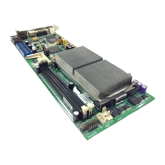
Unpacking Checklist 1. Take out the NuPRO-861 series unit from the carton box, check if the unit is properly secure in the plastic bag. 2. Check the contents of the carton box: Industrial board Installation guide ATA-66/100 HDD ribbon cable Floppy ribbon cable Print &... - Page 9 (5-pins to 6-pins) Low profile heat sink with fan Note: The package of the NuPRO-861 OEM version non-standard configuration may vary in function or contents according to different configuration requests CAUTION: This board must be protected from static discharge and physical shock.
-
Page 10: Features
Hardware Monitoring Hardware monitoring allows the user to monitor various aspects of their systems operations and status. The features include CPU temperature, voltage and RPM of fan. Moreover, the NuPRO-861 with jumper can adjust the fan speed. 4 • Introduction... - Page 11 I/O Shield Connector The SBC is equipped with an I/O bracket. Please use the appropriate I/O shield. Figure 1: I/O back panel layout NuPRO-861 Series Overview Function NuPRO-861 ® Chipset Intel 855GME LVDS function DVI function VGA function Gigabit Ethernet function...
-
Page 12: Functional Block
Functional Block The following topics provide an overview of the NuPRO-861 main features as shown in the functional block diagram below and also the main board. Functional Block Diagram Socket 478-pins Clock Intel Pentium M ADDR CTRL DATA 400/533 MHz FSB... -
Page 13: Specifications
Specifications • Processor: • Intel ® ® Pentium M processor with socket 478-pins package • Processor operating at 1.3GHz and up to 1.8GHz System bus frequency at 400/533MHz FSB • Chipset: ® Intel 855GME + ICH4 AGPset • DRAM Module: •... - Page 14 • 1 x 16-pins CRT VGA port • 2 x Serial ports for RS-232 • 4 x USB2.0 connectors (USB cable with bracket) • BIOS: Award Plug and Play BIOS • Form Factor: 13.3” x 4.8” (338 x 122mm) • Weight: 0.84lb (380g) 8 •...
-
Page 15: Chapter 2 Installation
Installation System Installation CPU Installation Carefully follow the steps below to install the CPU: Check and confirm that the jumpers are correctly set for the CPU being installed (figure 3). Lift the releasing lever of the Socket 478. Align the pins of the CPU with the pinholes of the Socket 478. Be sure to pay attention to the orientation of the CPU. - Page 16 CPU cooling fan. Removing a CPU: Before removing the CPU, turn off the NuPRO-861 Series power; then wait for about 20 minutes until the heat radiation plate of the cooling fan and the CPU cools down.
- Page 17 Do not touch the connector of the DIMM. Dirt residues may cause malfunctions. Hold the DIMM with its notch to the front side of the NuPRO-861 Series and insert it completely into the socket. A DIMM should be inserted into the inner socket first.
- Page 18 Setting Jumpers and DIP Switches There are jumpers and DIP-switches on the Embedded Board of the NuPRO-861 Series. You can set the jumpers to make the necessary operations. Figure 7: Jumper Connector For three-pin jumpers (Figure 7), the jumper setting is 1-2 when the jumper connects pins 1 and 2.
-
Page 19: Board Layout
Board Layout CN20 CN15 CN17 CN11 CN19 USB2/3 CN16 USB0/1 CN1 CN5 LVDS CN14 CN13 CN12 CN4 CN10 Figure 8: Jumper and Connector Locations Installation • 13... -
Page 20: Jumper Setting
Jumper setting Jumper Location Description: Use the information in the following table to change the jumpers and the DIP switches. Jumpers Functions Clear CMOS Setting Select CPU Type Setting Select Watchdog Timer Setting Select A description on setting the jumpers to enable/disable or change functions To set up the correct configuration is . - Page 21 Watchdog Timer Setting Select: JP3 Function Reset System (Default) Location: Installation • 15...
-
Page 22: Connectors Description
Connectors Description CN20 CN15 CN17 CN11 CN19 USB2/3 CN16 USB0/1 CN1 CN5 LVDS CN14 CN13 CN12 CN4 CN10 Figure 9: Connector Location 16 • Installation... - Page 23 Table for Connector’s Location Description: Use the information in the following table to change the connector. Connectors Functions Secondary IDE Connector Parallel Port Connector System Panel Indicate Connector IrDA Connector Primary IDE Connector Floppy Disk Connector COM1 RS-232 Serial Port Connector USB 0/1 (Pin-Header) Connector USB 2/3 (Pin-Header) Connector CN10...
- Page 24 Secondary IDE Connector (40-pins 2.54mm Pitch Pin-Header with Housing): CN1 Assignment Assignment Reset IDE Ground Host Data 7 Host Data 8 Host Data 6 Host Data 9 Host Data 5 Host Data 10 Host Data 4 Host Data 11 Host Data 3 Host Data 12 Host Data 2 Host Data 13...
- Page 25 Parallel Port Connector (26-pins 2.54mm Pitch Pin-Header with Housing): CN2 Assignment Assignment Line Printer Strobe Auto Feed PD 0, Parallel Data 0 Error PD 1, Parallel Data 1 Initialize PD 2, Parallel Data 2 Select PD 3, Parallel Data 3 Ground PD 4, Parallel Data 4 Ground...
- Page 26 ATX PWRON 5VSB PWR ON PWRBT+ (Dual 5V) PWRBT- (Ground) Figure 12: System Panel Indicate Connector IrDA Connector (5-pins Pin-Header): CN4 Assignment FIRTX IRRX Ground IRTX Figure 13: IrDA Connector 20 • Installation...
- Page 27 Primary IDE Connector (40-pins 2.54mm Pitch Pin-Header with Housing): CN5 Assignment Assignment Reset IDE Ground Host Data 7 Host Data 8 Host Data 6 Host Data 9 Host Data 5 Host Data 10 Host Data 4 Host Data 11 Host Data 3 Host Data 12 Host Data 2 Host Data 13...
- Page 28 Floppy Disk Connector (34-pins 2.54mm Pitch Pin-Header with Housing): CN6 Assignment Assignment Ground Drive Density Selection Ground Ground Ground Index Ground Motor Enable 0 Ground Drive Select 1 Ground Drive Select 0 Ground Motor Enable 1 Ground Direction Ground Step Ground Write Data Ground...
- Page 29 Figure 16: COM1 RS-232 Serial Port Connector USB 0/1 Connector (9-pins Pin-Header): CN8 Assignment Assignment USB0N USB1N USB0P USB1P Ground Ground Figure 17: USB 0/1 Connector USB 2/3 Connector (9-pins Pin-Header): CN9 Assignment Assignment USB2N USB3N USB2P USB3P Ground Ground Figure 18: USB 2/3 Connector Installation •...
- Page 30 ATX Control Power Connector: CN10 Pin # Assignment 5VSB ATX_PWRON Ground Figure 19: ATX Control Power Connector COM2 RS-232 Serial Port Connector (10-pins Pin-Header): CN11 Assignment Assignment Ground Ground Figure 20: COM2 RS-232 Serial Port Connector System fan power connector: CN12 Pin # Assignment Ground...
- Page 31 Figure 21: System Fan Power Connector CPU fan power connector: CN13 Pin # Assignment Ground Fan Status Signal Figure 22: CPU fan power connector 18/24 Bits LVDS Panel Interface (40-pins Male): CN14 Assignment Assignment Ground Ground YAM0 YAM1 YAP0 YAP1 Ground Ground YAM2...
- Page 32 +12V +12V PVCC PVCC Figure 23: 18/24 Bits LVDS Panel Interface Gigabit Ethernet RJ-45 Connector (RJ-45 Phone–Jack): CN15 Assignment Assignment LINK1000# LINK100# LINK# Ground ACT# Ground NPTH1 NPTH2 Figure 24: Gigabit Ethernet RJ-45 Connector 26 • Installation...
- Page 33 Audio Port Connector (9-pins Pin-Header): CN16 Assignment +12V 3.3V AC_SYNC AC_SDOUT Ground AC_BCLK Ground AC_RST# AC_SDIN0 Figure 25: Audio Port Connector CRT VGA Port Connector (16-pins Pin-Header): CN17 Assignment Assignment Green Ground Blue Data Ground HSync Ground VSync Ground Clock Ground Figure 26: CRT VGA Port Connector Installation •...
- Page 34 DVI Port Connector (30-pins Pin-Header): CN18 Assignment Assignment TX2- HPDET TX2+ TX0- Ground TX0+ Ground DATA CLOCK Ground CRT_VS TXC+ TX1- TXC- TX1+ CRT_RED Ground CRT_GREEN CRT_BLUE CRT_HS DVI_5V Ground Ground Ground Figure 27: DVI Port Connector External Keyboard Connector (5-pins Pin-Header): CN19 Assignment Assignment Keyboard CLOCK...
- Page 35 PS/2 Keyboard & Mouse Connector (6-pins Mini Din): CN20 Assignment Assignment Keyboard DATA Mouse DATA Ground Keyboard CLOCK Mouse CLOCK Figure 29: PS/2 Keyboard & Mouse Connector Type II CompactFlash Connector: CF Assignment Assignment Ground CS#1 Ground Ground Ground Ground Ground Ground Ground...
-
Page 36: Optional Ip-Alcs20 Audio Card
IDEACTS# Ground Ground Ground Figure 30: Type II CompactFlash Connector: CF 2.5 Optional IP-ALCS20 Audio Card Thank you for choosing IP-ALCS20 Audio Card. Instructions on connecting the connector and the phone jack for audio functions are detailed below. IP-ALCS20 Rev 1.0 CD_IN Figure 31: Board Location 30 •... - Page 37 Check the contents of the packing: • IP-ALCS20 Audio Card • Audio 9-pins round cable Audio Card Descriptions of Connector: Connectors Functions CD_IN Connector Audio Line_In, Line_Out, MIC Phone Jack Audio Signal Connector Description of Connector CD_IN Connector: JP1 Assignment Left Ground Ground...
- Page 38 AC_SDOUT Ground AC_BCLK Ground AC_RST# AC_SDIN0 32 • Installation...
-
Page 39: Chapter 3 Award Bios Setup
Award BIOS Setup BIOS Instructions Award’s ROM BIOS provides a built-in Setup program, which allows the user to modify the basic system configuration and hardware parameters. The modified data will be stored in a battery-backed CMOS, so that data will be retained even when the power is turned off. - Page 40 Esc: Quit ↑ ↓ →←: Select Item F10: Save & Exit Setup Time, Date, Hard Disk Type…. Note: A brief description of each highlighted selection appears at the bottom of the screen. Setup Items: The main menu includes the following main setup categories. Recall that some systems may not include all entries.
-
Page 41: Standard Cmos Features
Load Fail-Safe Defaults: Use this menu to load the BIOS default values for the minimal/stable performance for the system to operate. Please refer to section 3.12 for further information. Load Optimized Defaults: Use this menu to load the BIOS default values that are factory settings for optimal performance system operations. - Page 42 Date (mm:dd:yy): Mon, Aug 4 Item Help Time (hh:mm:ss): 2003 __________________________ 16:19:20 IDE Primary Master IDE Primary Slave Menu Level 13579 MB IDE Secondary Master None IDE Secondary Slave Change the day, month, year and None century None Drive A Drive B 1.44M, 3.5 in.
-
Page 43: Ide Adaptors
Select the default video device. Halt On: Options All Errors/No Errors/All, but Keyboard/All, but Diskette/All, but Disk/Key Select the situation in which the user wants the BIOS to stop the POST process and notify the user. Base Memory: Option N/A Displays the amount of conventional memory detected during boot up. -
Page 44: Advanced Bios Features
fills the remaining fields on this menu. IDE Primary Master: Options: None, Auto, and Manual Selecting “Manual” allows the user to set the remaining fields on this screen. "User Type" allows the user to select the number of cylinders, heads, etc. Note: PRECOMP=65535 means NONE. - Page 45 CPU Feature Press Enter Item Help Hard Disk Boot Priority Press Enter __________________________ Virus Warning Enabled CPU L1 & L2 Cache Enabled Quick Power On Self Test Enabled Menu Level First Boot Device Floppy Second Boot Device Hard Disk Third Boot Device LS-120 Boot Other Device Enabled...
- Page 46 into this area, BIOS will show a warning message on the screen and an alarm will sound. Enabled - Activates automatically when the system boots up causing a warning message to appear when anything attempts to access the boot sector or hard disk partition table. Disabled - No warning message will appear when anything attempts to access the boot sector or hard disk partition table.
- Page 47 Boot Up NumLock Status: Select power on state for NumLock. Options: On, Off Gate A20 Option: Select if chipset or keyboard controller should control GateA20. Normal - A pin in the keyboard controller controls GateA20 Fast - Lets chipset control GateA20 Security Option: Select whether the password is required every time the system boots or only when entering setup.
-
Page 48: Advanced Chipset Features
Advanced Chipset Features This section allows the user to configure the system based on the specific features of the installed chipset. This chipset manages bus speeds and access to system memory resources, such as DRAM and the external cache. It also coordinates communications between the conventional ISA bus and the PCI bus. - Page 49 on the DRAM timing. Options: 2, 2.5 Active To Precharge Delay: Select the operating system that is active to precharge delay. Options: 5, 6, 7. DRAM RAS# To CAS# Delay: This field allows the user to insert a timing delay between the CAS and RAS strobe signals, used when DRAM is written to, read from, or refreshed.
- Page 50 Options: Enabled, Disabled. Memory Hole At 15M-16M: The user can reserve this area of system memory for ISA adapter ROM. When this area is reserved, it cannot be cached. The user information of peripherals that need to use this area of system memory would have normally discussed their memory requirements. Options: Enabled, Disabled.
-
Page 51: Integrated Peripherals
Integrated Peripherals Phoenix - AwardBIOS CMOS Setup Utility Integrated Peripherals Onboard IDE Device Press Enter Item Help Onboard Device Press Enter __________________________ SuperIO Device Press Enter Onboard Lan Boot ROM Disabled Onboard Serial Port 3 Menu Level Serial Port 3 Use IRQ IRQ10 If your IDE hard drive supports Onboard Serial Port 4... - Page 52 mode (0-4) for each of the four IDE devices that the onboard IDE interface supports. Modes 0 through 4 provide successively increased performance. In Auto mode, the system automatically determines the best mode for each device. Options: Auto, Mode 0, Mode 1, Mode 2, Mode 3, and Mode 4. IDE Primary/Secondary Master/Slave UDMA: Ultra DMA/33 implementation is possible only if the IDE hard drive supports it and the operating environment includes a DMA driver (Windows 95 OSR2 or a...
- Page 53 USB Mouse Support: Select “Enabled” if the user’s system contains a Universal Serial Bus (USB) controller and have a USB mouse. Options: Enabled, Disabled. AC97 Audio: This item allows the user to decide to auto or disable the chipset family to support AC97 Audio.
- Page 54 SuperIO Device: SuperIO Device Power ON Function BUTTON ONLY Item Help Hot Key Power ON Ctrl-F1 ____________________________ Onboard FDC Controller Enabled Onboard Serial Port 1 3F8/IRQ4 Menu Level Onboard Serial Port 2 2F8/IRQ3 UART Mode Select Normal X RxD, TxD Active Hi, Lo X IR Transmission Delay Enabled...
- Page 55 UART Mode Select: This item allows the user to select UART mode. Options: IrDA, ASKIR, and Normal. RxD, TxD Active: This item allows the user to determine the active of RxD, TxD. Options: “Hi, Hi”, “Lo, Lo”, “Lo, Hi” and “Hi, Lo”. IR Transmission delay: This item allows the user to enable/disable IR transmission delay.
-
Page 56: Power Management Setup
PWRON After PWR-Fail: This item allows the user to power on the system after power failure. Options: Off, On, and Former-Sts. Onboard Lan Boot ROM: Select “Enabled” if the system has a LAN device installed on the system board. Options: Enabled, Disabled. Onboard Serial Port 3/Port4: Select an address for the third and forth serial ports. - Page 57 ACPI Function: This item allows you to enable or disable the Advanced Configuration and Power Management(ACI). The choice: Enabled, Disabled. Power Management: This category allows you to select the type (or degree) of power saving and is directly related to the following modes: 1.
- Page 58 This determines the manner in which the monitor is blanked. Options: Yes, No. Suspend Type: Select the Suspend Type. Options: PWRON Suspend, Stop Grant. 52 • Award BIOS Setup...
- Page 59 Suspend Mode: When “Enabled” and after the set time of system inactivity. All devices except the CPU will be shut off. Options: Enabled, Disabled. HDD Power Down: When “Enabled” and after the set time of system inactivity, the hard disk drive will be powered down while all other devices remain active.
-
Page 60: Plug And Play / Pci Configurations
Plug and Play / PCI Configurations This section describes how to configure the PCI bus system. PCI, or Personal Computer Interconnect, is a system which allows I/O devices to operate at speeds close to the speed the CPU uses when communicating with its own special components. -
Page 61: Pc Health Status
PCI/VGA Palette Snoop: Leave this field at “Disabled”. Options: Enabled, Disabled. 3.10 PC Health Status Phoenix - AwardBIOS CMOS Setup Utility PC Health Status CPU Warning Temperature Disabled Item Help Temperature 24°C / 75°F ____________________________ Temperature 40°C / 104°F SYSFAN 3283RPM Menu Level CPU FAN... -
Page 62: Frequency/Voltage Control
CPUFAN: Shows the current CPU fan operating speed. VDIMM (V) Shows the voltage level of the DRAM. VCORE (V) Shows the voltage level of CPU (Vcore). +3.3V/+5V/+12V/-12V/-5V/5VSB(V): Shows the voltage of +5V/+12V/-12V/-5V. VBAT (V) Shows the voltage level of the battery. Shutdown Temperature: This item allows the user to set up the CPU shutdown Temperature. -
Page 63: Load Fail-Safe Defaults
Spread Spectrum Modulated: This item allows the user to enable or disable the Spread Spectrum Modulated. Options: Disabled, -0.25%, -0.50%, and -0.75%. 3.12 Load Fail-Safe Defaults When <Enter> is pressed on this item a confirmation dialog box will appear with a message similar to: Load Fail-Safe Defaults (Y/N)? N Pressing ‘Y’... -
Page 64: Exit Selecting
appear in the middle of the screen prompting the user to create a password. ENTER PASSWORD: Type the password, up to eight characters in length, and press <Enter>. The password typed will now clear any previously entered password from CMOS memory. - Page 65 selections stored in CMOS. After saving the values the system is restarted again. Exit Without Saving Pressing <Enter> on this item will prompt for confirmation: Quit without saving (Y/N)? Y This allows the user to exit Setup without saving any changes made in CMOS. The previous selections remain in effect.
-
Page 67: Warranty Policy
Warranty Policy Thank you for choosing ADLINK. To understand your rights and enjoy all the after-sales services we offer, please read the following carefully: Before using ADLINK’s products please read the user manual and follow the instructions exactly. When sending in damaged products for repair, please attach an RMA application form.
Need help?
Do you have a question about the NuPRO-861 and is the answer not in the manual?
Questions and answers