Table of Contents
Advertisement
Quick Links
Advertisement
Table of Contents

Related Manuals for Advantech PCI-1721


Summary of Contents for Advantech PCI-1721
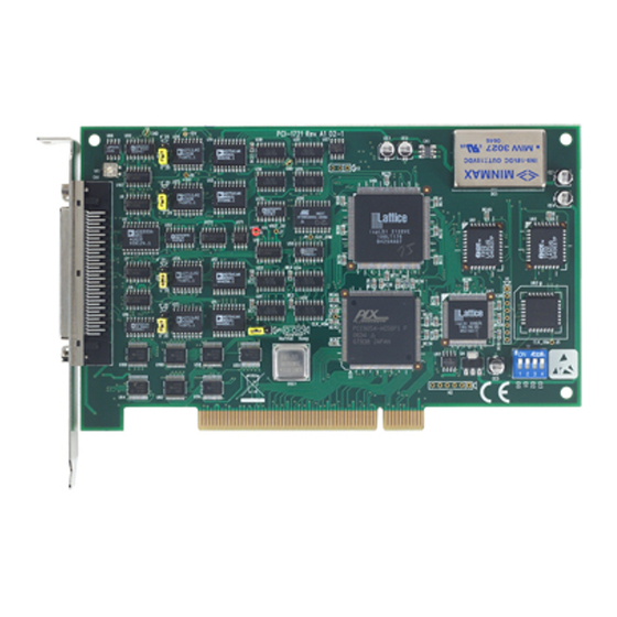
- Page 1 PCI-1721 12-bit, 4-channel Advanced Analog Output Card...
- Page 2 Acknowledgments PC-LabCard is a trademark of Advantech Co., Ltd. IBM and PC are trade- marks of International Business Machines Corporation. MS-DOS, Win- dows, Microsoft Visual C++ and Visual BASIC are trademarks of Microsoft Corporation.
-
Page 3: Table Of Contents
Contents 1. Introduction ................1 1.1 Features ..................1 1.2 Applications ................. 4 1.3 Installation Guide ................4 1.4 Software Overview ................ 6 1.5 DLL Driver Programming Roadmap ..........7 1.6 Accessories .................. 9 2. Installation ................10 2.1 Unpacking .................. 10 2.2 Switch and Jumper Settings ............ - Page 4 C.10 Calibration Status - BASE+28H ..........38 C.11 I/O Setting Command and Status - BASE+2AH ......39 C.12 Clear FIFO strobe - BASE+2CH ..........40 C.13 Clear FIFO strobe - BASE+2EH ..........40 C.14 82C54 Counter Chip - BASE+30/32/34/36H ......... 41 C.15 DIO Write/Read- BASE+3EH ............
-
Page 5: Introduction
Chapter 1 Thank you for buying the Advantech PCI-1721. The PCI-1721 is an advanced high-speed analog output card for PCI bus, and each of analog output channels is equipped with a 12-bit, double-buffered DAC. It features many powerful and unique functions, like waveform output function with 10 MHz maximum update rate, auto-calibration function and Board ID. - Page 6 10MS/s for each analog output channel. Or you can load a cyclic waveform into an on-board FIFO, which will continuously output the cyclic waveform. The on-board FIFO of the PCI-1721 can store 2 to 1024 samples of the waveform. Users can independently set the four outputs to different ranges: 0~+5V, 0~+10V, ±5V, ±10V, 0~20mA or 4~20mA, and all the ranges are...
- Page 7 Chapter 1 The PCI-1721 has a built-in DIP Switch that helps define each card’s ID when multiple PCI-1721 cards have been installed on the same PC chassis. The board ID setting function is very useful when users build their system with multiple PCI-1721 cards. With correct Board ID settings, you can easily identify and access each card during hardware configuration and software programming.
-
Page 8: 1.2 Applications
Programmable current sink Servo control Multiple loop PID control Simulate function generator 1.3 Installation Guide Before you install your PCI-1721 card, please make sure you have the following necessary components: PCI-1721 DA&C card PCI-1721 User’s Manual Driver software Advantech DLL drivers... - Page 9 Chapter 1 Fig. 1-1 Installation Flow Chart Advantech Co., Ltd. – 5 – PCI-1721 User’s Manual www.advantech.com...
-
Page 10: Software Overview
The Advantech DLL Drivers software is included on the companion CD-ROM at no extra charge. It also comes with all the Advantech DA&C cards. Advantech’s DLL driver features a complete I/O function library to help boost your application performance. The Advantech... -
Page 11: Dll Driver Programming Roadmap
C++ Builder For instructions on how to begin programming works in each develop- ment tool, Advantech offers a Tutorial Chapter in the DLL Drivers Manual for your reference. Please refer to the corresponding sections in this chapter on the DLL Drivers Manual to begin your programming efforts. - Page 12 Or you can refer to the DLL Driver Error Codes Appendix in the DLL Drivers Manaul for a detailed listing of the Error Code, Error ID and the Error Message. Advantech Co., Ltd. PCI-1721 User’s Manual – 8 – www.advantech.com...
-
Page 13: 1.6 Accessories
Chapter 1 1.6 Accessories Advantech offers a complete set of accessory products to support the PCI-1721 card. These accessories include: Wiring Cable PCL-10168 The PCL-10168 shielded cable is specially designed for PCI-1721 cards to provide high resistance to noise. To achieve a better signal quality, the signal wires are twisted in such a way as to form a “twisted-... -
Page 14: Installation
This chapter gives users a package item checklist, proper instructions about unpacking and step-by-step procedures for both driver and card installation. After receiving your PCI-1721 package, please inspect its contents first. The package should contain the following items: PCI-1721 card Companion CD-ROM (DLL driver included) User’s Manual... - Page 15 Keep the anti-static bag for future use. You might need the original bag to store the card if you have to remove the card from PC or transport it elsewhere. Advantech Co., Ltd. – 11 – PCI-1721 User’s Manual www.advantech.com...
-
Page 16: Switch And Jumper Settings
Complete loss of power to the chip clears the chip memory. Thus, no matter how JP1 is set, if the power to the PCI-1721 is disconnected, the analog output initial power-on state will be “ZERO”. - Page 17 DIO4 DIO5 DIO6 DIO7 DIO8 DIO9 DIO10 DIO11 DIO12 DIO13 DIO14 DIO15 DGND DGND CNT0_CLK FIFO_OUT CNT0_OUT EXT_GATE CNT0_GATE EXT_CLK +12V Fig. 2-2 I/O connector pin assignments for the PCI-1721 Advantech Co., Ltd. – 13 – PCI-1721 User’s Manual www.advantech.com...
-
Page 18: I/O Connector
Note: +12 V and +5 V can't be used as the reference voltage of Iout. CLK_10M FIFO_C0 FIFO_C1 82C54 82C54 Waveform CNT1 CNT2 Mode 10 M EXT_CLK EXT_GATE FIFO_CLK FIFO_WR FIFO Fig. 2-3 FIFO block diagram of PCI-1721 Advantech Co., Ltd. PCI-1721 User’s Manual – 14 – www.advantech.com... -
Page 19: Driver Installation
Chapter 2 We recommend you to install the driver before you install the PCI-1721 card into your system, since this will guarantee a smooth installation process. The 32-bit DLL driver Setup program for the PCI-1721 card is included on the companion CD-ROM that is shipped with your DA&C card package. -
Page 20: Hardware Installation
(please refer to 2.4 Driver Installation) After the DLL driver installation is completed, you can now go on to install the PCI-1721 card in any PCI slot on your computer. But it is suggested that you should refer to the computer user manual or related documentation if you have any doubt. - Page 21 Device Manager: 1. Access the Device Manager through Control Panel/System/Device Manager. 2. The device name of the PCI-1721 should be listed on the Device Manager tab on the System Property Page. Advantech Co., Ltd.
- Page 22 A complete device installation procedure should include device setup, configuration and testing. The following sections will guide you through the Setup, Configuration and Testing of your device. Advantech Co., Ltd. PCI-1721 User’s Manual – 18 – www.advantech.com...
-
Page 23: Device Setup & Configuration
Advantech 32-bit DLL drivers. Step 1: To install the I/O device for your card, you must first run the Device Installation program (by accessing Start/Programs/ Advantech Driver for 95 and 98 (or for NT/2000)/Device Installation). Fig. 2-7 The Advantech Device Installation utility program... - Page 24 OK button. After you have clicked OK, you will see a Device Setting dialog box such as the one in Fig. 2-10. Fig. 2-9 The “Device(s) Found” dialog box Advantech Co., Ltd. PCI-1721 User’s Manual – 20 – www.advantech.com...
- Page 25 : By inputting an external reference voltage: -xV , where |x| <= 10, you will get a output voltage range: 0 to xV. Advantech Co., Ltd. – 21 – PCI-1721 User’s Manual www.advantech.com...
- Page 26 Fig. 2-11 The Device Name appearing on the list of devices box Note: As we have noted, the device name “000:PCI-1721 I/O=6600H” begins with a device number “000”, which is specifically assigned to each card. The device number is passed to the driver to specify which device you wish to control.
-
Page 27: Signal Connections
PCI-1721 via the I/O connector. The PCI-1721 provides four D/A output channels, Vout_0 ~ Vout_3 and Iout_0 ~ Iout_3. Users may use the PCI-1721 internally-provided precision -5V (-10V) reference to generate 0 to +5 V (+10 V) D/A output range. -
Page 28: Trigger Source Connections
32-bit timer for pacer triggering. A low-to-high edge from the Counter 2 output (PACER_OUT) will trigger an A/D conversion on the PCI-1721. At the same time, you can also use this signal as a synchronous signal for other applications. -
Page 29: Field Wiring Considerations
Chapter 3 When you use the PCI-1721 to acquire data from outside, noises in the environment might significantly affect the accuracy of your measure- ments if due cautions are not taken. The following measures will be helpful to reduce possible interference running signal wires between signal sources and the PCI-1721. -
Page 30: Appendix A. Specifications
16 (bi-directional) Number of ports 0.8 V max. Input Voltage High 2.0 V min. 0.5 V max. @ +24 mA (sink) Output Voltage High 2.0 V min. @ -15 mA (source) Advantech Co., Ltd. PCI-1721 User’s Manual – 26 – www.advantech.com... - Page 31 +12 V @ 700 mA 0~+60° C (32~140° F) Operation (refer to IEC 68-2-1,2) Temperature Storage -20~+85° C (-4~185° F) Relative Humidity 5~95%RH non-condensing (refer to IEC 68-2-3) Certification CE certified Advantech Co., Ltd. – 27 – PCI-1721 User’s Manual www.advantech.com...
-
Page 32: Appendix B. Block Diagram
DA C 0 OSC. VOUT0 REF_V0 IOUT1 12Bit DA C 1 VOUT1 REF_V1 IOUT2 12Bit DA C 2 VOUT2 REF_V2 IOUT3 12Bit DA C 3 VOUT3 REF_V3 Auto Calibration Circuit Advantech Co., Ltd. PCI-1721 User’s Manual – 28 – www.advantech.com... -
Page 33: Appendix C. Register Structure And Format
For example, BASE+0 is the card’s base address and BASE+7 is the base address plus seven bytes. The table C-1 shows the function of each register of the PCI-1721 or driver and its address relative to the card’s base address. - Page 34 Appendix C Table C-1 PCI-1721 register format (Part 1) Base PCI-1721 Register Format Address + HEX D/A Channel 0 Data DA11 DA10 D/A Channel 1 Data DA11 DA10 D/A Channel 2 Data DA11 DA10 D/A Channel 3 Data DA11 DA10...
- Page 35 Appendix C Table C-1 PCI-1721 register format (Part 2) Base PCI-1721 Register Format Address + HEX All D/A channels Synchronized Setting Command SYNC All D/A channels Synchronized Setting Status SYNC Synchronization Strobe Calibration Setting Command SEL1 SEL0 Calibration Setting Status...
- Page 36 Appendix C Table C-1 PCI-1721 register format (Part 3) Base PCI-1721 Register Format Address + HEX 82C54 Counter 0 Command 82C54 Counter 0 Status 82C54 Counter 1 Command 82C54 Counter 1 Status 82C54 Counter 2 Command 82C54 Counter 2 Status...
-
Page 37: D/A Channel 0/1/2/3 Data - Base+0/2/4/6H
(LSB) of the D/A data DA11 the most significant bit (MSB) The PCI-1721 offers Board ID register BASE+10H. With correct Board ID settings, user can easily identify and access each card during hardware configuration and software programming. -
Page 38: D/A Control - Base+12H
Appendix C Table C-4 PCI-1721 Register for D/A control Base Addr. D/A Control Command VREF VREF VREF VREF UB_3 UB_2 UB_1 UB_0 D/A Control Status VREF VREF VREF VREF UB_3 UB_2 UB_1 UB_0 D/A channel n output voltage range UB_n... -
Page 39: Write Calibration Result To Eeprom - Base+16H
Appendix C Table C-5 PCI-1721 Register for write calibration result to EEPROM Base Addr. Write Calibration Result to EEPROM SEL1 SEL0 D7 ~ D0 Calibration result data the least significant bit (LSB) of the data the most significant bit (MSB) -
Page 40: All D/A Channels Synchronized Setting - Base+22H
Appendix C The PCI-1721 provides the innovation function which all D/A channels can output the data synchronization. Table C-6 PCI-1721 Register for all D/A channels synchronized setting Base Addr. All D/A channels Synchronized Setting Command SYNC All D/A channels Synchronized Setting Status... -
Page 41: Calibration Setting - Base+26H
Appendix C Table C-8 PCI-1721 Register for calibration command and status Base Addr. Calibration Setting Command SEL1 SEL0 Calibration Setting Status SEL1 SEL0 D7 ~ D0 Calibration result data the least significant bit (LSB) of the data the most significant bit (MSB) - Page 42 Appendix C Table C-9 PCI-1721 Register for calibration status Base Addr. Calibration Status CALI_ CALI_ CALI_ INIT CALI_RDY Calibration activate bit This bit indicates whether the calibration command is finish. 0 means that the calibration command is finish. CALI_INIT Calibration initial bit This bit indicates whether the calibration controller is initialed.
- Page 43 Appendix C Table C-10 PCI-1721 Register for I/O setting Base Addr. I/O Setting Command FIFO_ FIFO_ 8254_ HDIO LDIO GATE0 CNT0 I/O Setting Status FIFO_ FIFO_ 8254_ HDIO LDIO GATE0 CNT0 8254_CNT0 Select clock source of 82C54 counter 0 10 MHz clock...
- Page 44 Appendix C Write any values to BASE+2CH to clear the FIFO. Table C-11 PCI-1721 Register for clear FIFO strobe Base Addr. Clear FIFO strobe Table C-12 PCI-1721 Register for clear FIFO strobe Base Addr. FIFO Status FIFO Empty flag This bit indicates whether the FIFO is empty.
- Page 45 Appendix C Table C-13 PCI-1721 Register for82C54 counter chip Base Addr. 82C54 Counter 0 Command 82C54 Counter 0 Status 82C54 Counter 1 Command 82C54 Counter 1 Status 82C54 Counter 2 Command 82C54 Counter 2 Status 82C54 Control Command 82C54 Control Status The four registers of BASE+30/32/34/36H are used for the 82C54 ®...
- Page 46 Base Addr. Write DO data Read DI data The PCI-1721 provides the 32-bit FIFO. Write the data (pattern) which you want to output to BASE+40/42H, then the data will transfer to the FIFO. Table C-15 PCI-1721 Register for DMA FIFO data buffer Base Addr.
- Page 47 If you installed the program to another directory, you can find these programs in the corresponding subfolders in your destination directory. The PCI-1721 has been calibrated at the factory for initial use. How- ever, a calibration of the analog input and the analog output function every six months is recommended.
- Page 48 Appendix D There is one variable resistor (VR1) on the PCI-1721 to adjust the accurate reference voltage on the PCI-1721. We have provided a test point (See J6 in Figure D-1) for you to check the reference voltage on board. Before you start to calibrate A/D and D/A channels, please adjust VR1 until the reference voltage on J6 has reached +10.0000 V.
- Page 49 1 LSB. 8. To change to another channel and repeat steps 2 to 7 to calibrate all four channels. Advantech Co., Ltd. – 45 – PCI-1721 User’s Manual www.advantech.com...
- Page 50 D/A calibration. The program helps the user to easily finish the calibration procedures automatically, however, the user can calibrate the PCI-1721 manually. The following steps will guide you through the PCI-1721 software calibration. Step 1: Access the calibration utility program AutoCali.exe from the...
- Page 51 Step 2: Select PCI-1721 in the ADSDAQ dialog box. Figure D-2: Selecting the device you want to calibrate Step 3: After you start to calibrate the PCI-1721, please don’t forget to adjust VR1. Figure D-3: Warning message before start calibration Advantech Co., Ltd.
- Page 52 Appendix D Step 4: There are four D/A channels in PCI-1721, select the output range for each channel and then press the Start button to calibrate D/A channels (Fig. D-4). Figure D-4: Range Selection in D/A Calibration Step 5: Clicking the Start button, the utility will test some registers to make sure the PCI-1721 has stable enough to process the calibrate procedure (Fig.
- Page 53 Step 6: D/A channel 0 calibration is enabled (Fig. D-6) Figure D-6: Calibrating D/A Channel 0 Step 7: D/A channel 1 calibration is enabled (Fig. D-7) Figure D-7: Calibrating D/A Channel 1 Advantech Co., Ltd. – 49 – PCI-1721 User’s Manual www.advantech.com...
- Page 54 Step 2: For example, choose channel 0; select the Range and select the wished output voltage code or value from the radio buttons (Fig. D-9 and Fig. D-10). Figure D-9: Selecting D/A Range Advantech Co., Ltd. PCI-1721 User’s Manual – 50 – www.advantech.com...
- Page 55 Step 3: According to the difference between the output voltage from D/A channel and the value in the multi-meter, adjust the gain and offset registers (Fig. D-11) Figure D-11: Adjusting registers Advantech Co., Ltd. – 51 – PCI-1721 User’s Manual www.advantech.com...
- Page 56 Step 4: Adjust registers until they fall between the output voltage from the D/A channel and the value in the multi-meter. Note: ✎ The “Waveform Editor Utility” also comes with PCI-1721. Access this program from the default location: C:\Program Files\Advantech\ADSAPI\Utility\PCI-1721\WaveformEditor Kindly refer to the “readme”...
Need help?
Do you have a question about the PCI-1721 and is the answer not in the manual?
Questions and answers