
Related Manuals for Intel Altera MAX 10 FPGA


Summary of Contents for Intel Altera MAX 10 FPGA
- Page 1 Explore more resources ® Altera Design Hub ® 10 FPGA Development Kit User Guide 683460 Online Version Send Feedback 2024.11.20 UG-01169...
-
Page 2: Table Of Contents
2.3. Software and Driver Installation................8 2.3.1. Installing the Quartus Prime Software............8 2.3.2. Installing the Development Kit..............9 2.3.3. Installing the Intel FPGA Download Cable Driver...........10 2.4. Board Update Portal..................... 11 2.4.1. Step 1: Connect to the Board Update Portal..........11 2.4.2. - Page 3 Contents A.8.4. HSMC.....................49 A.8.5. Pmod Connectors..................53 A.8.6. USB to UART................... 54 A.9. Memory......................55 A.9.1. DDR3 Rev. B Board.................. 55 A.9.2. DDR3 Rev. C Board.................. 57 A.9.3. Flash......................59 A.10. Power Distribution System.................. 61 B. Developer Resources....................62 C. Safety and Regulatory Compliance Information............63 C.1.
-
Page 4: Overview
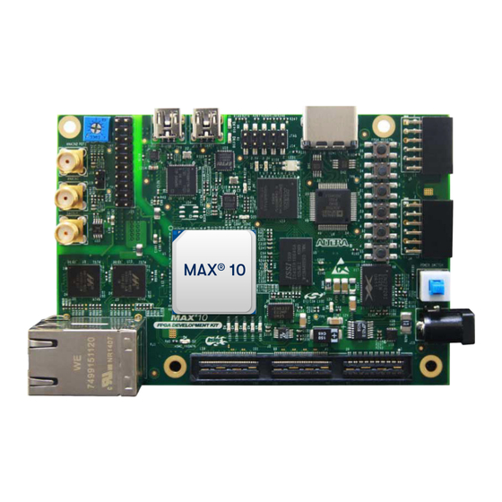
Altera or Intel. Altera and Intel customers are advised to obtain the latest version of device specifications before relying on any published information and before placing orders for products or services. - Page 5 1. Overview 683460 | 2024.11.20 Figure 2. MAX 10 FPGA Development Kit—Bottom View Note: To determine the revision of your board, look for the serial number at the bottom of the board. Refer to the Appendix A—Development Kit Components section for more details about the components on the MAX 10 FPGA Development Kit.
-
Page 6: Block Diagram
Integrated Inductor • Enpirion EP5358xUI 600 mA PowerSoC DC-DC Step-Down Converters with Integrated Inductor ® • MAX II CPLD – EPM1270M256C4N (On-board Intel FPGA Download Cable II) Programming and Configuration • Embedded Intel FPGA Download Cable II (JTAG) • Optional JTAG direct via 10-pin header Memory Devices •... -
Page 7: Box Contents
Clocking • 25 MHz single-ended, external oscillator clock source • Silicon Labs clock generator with programmable frequency GUI Cables Mini-USB cable for on-board Intel FPGA Download Cable II Power 2A power supply and cord Software ® Free Quartus Prime software (download software and license from website) 1.3. -
Page 8: Getting Started
Altera or Intel. Altera and Intel customers are advised to obtain the latest version of device specifications before relying on any published information and before placing orders for products or services. -
Page 9: Installing The Development Kit
1. Download the MAX 10 FPGA Development Kit installer package from the MAX 10 FPGA Development Kit webpage on the Intel website. 2. Unzip the MAX 10 FPGA Development Kit installer package. The package creates the directory structure shown in the figure below. -
Page 10: Installing The Intel Fpga Download Cable Driver
The development board includes integrated Intel FPGA Download Cable circuitry for FPGA programming. However, for the host computer and board to communicate, you must install the On-Board Intel FPGA Download Cable II driver on the host computer. Installation instructions for the On-Board Intel FPGA Download Cable II driver for your operating system are available on the Intel website. -
Page 11: Board Update Portal
Intel website and to load software files into the Quad SPI flash memory on your board.The following steps ensure that you have the latest software available on both your computer and your board. -
Page 12: Step 2: Update The User Software Portion
2. Getting Started 683460 | 2024.11.20 Note: If you cannot connect to the Board Update Portal, refer to the file under readme.txt <package rootdir> directory on how you can recover the factory \factory_recovery build. 2.4.2. Step 2: Update the User Software Portion To update the user software portion of flash memory on your board, follow these steps: 1. -
Page 13: Board Test System
Altera or Intel. Altera and Intel customers are advised to obtain the latest version of device specifications before relying on any published information and before placing orders for products or services. -
Page 14: Using The Configure Menu
3. Board Test System 683460 | 2024.11.20 The BTS communicates over the JTAG bus to a test design running in the FPGA. The Board Test System and Power Monitor share the JTAG bus with other applications like the Nios II debugger and the Signal Tap Logic Analyzer. Because the Quartus Prime programmer uses most of the bandwidth of the JTAG bus, other applications using the JTAG bus might time out. -
Page 15: The System Info Tab
3. Board Test System 683460 | 2024.11.20 3.2. The System Info Tab The System Info tab shows the board’s current configuration. The tab displays the JTAG chain, the board’s MAC address, the Qsys memory map, and other details stored on the board. Figure 7. - Page 16 3. Board Test System 683460 | 2024.11.20 Controls Description Ethernet B MAC Indicates the Ethernet B MAC address of the board. JTAG Chain Shows all the devices currently in the JTAG chain. Qsys Memory Map Shows the memory map of the Platform Designer (Standard) system on your board.
-
Page 17: The Gpio Tab
3. Board Test System 683460 | 2024.11.20 3.3. The GPIO Tab The GPIO tab allows you to interact with all the general purpose user I/O components on your board. You can read DIP switch settings, turn LEDs on or off, and detect push button presses. -
Page 18: The Flash Tab
3. Board Test System 683460 | 2024.11.20 3.4. The Flash Tab The Flash tab allows you to read and write flash memory on your board. Figure 9. The Flash Tab (Detail) Table 5. Controls on the Flash Tab Control Description Read Reads the flash memory on your board. -
Page 19: The Hsmc Tab
3. Board Test System 683460 | 2024.11.20 3.5. The HSMC Tab The HSMC tab allows you to test the CMOS port. Figure 10. The HSMC Tab Table 6. Controls on the HSMC Tab Control Description Status Pattern sync: Shows the pattern synced or not synced state. The pattern is considered synced when the start of the data sequence is detected. - Page 20 3. Board Test System 683460 | 2024.11.20 Control Description • prbs31: Selects pseudo-random 31-bit sequences. • high_frequency: Divide by data pattern. • low_frequency: Divide by data pattern. Error Control • Detected errors: Displays the number of data errors detected in the hardware.
-
Page 21: The Ddr3 Tab
3. Board Test System 683460 | 2024.11.20 3.6. The DDR3 Tab The DDR3 tab allows you to test the DDR3 by reading and writing to a selected amount of addresses. Figure 11. The DDR3 Tab Table 7. Controls on the DDR3 Tab Control Description Performance Indicators... - Page 22 3. Board Test System 683460 | 2024.11.20 Control Description • Detected errors—Displays the number of data errors detected in the hardware. • Inserted errors—Displays the number of errors inserted into the transaction stream. • Insert Error—Inserts a one-word error into the transaction stream each time you click the button.
-
Page 23: The Adc Tab
3. Board Test System 683460 | 2024.11.20 3.7. The ADC Tab The ADC tab (analog-to-digital) shows the real-time voltage values of all of the ADC input channels. Figure 12. The ADC Tab The two tables displayed on this tab, ADC 1 and ADC 2, are not editable. The following tables show where the channels connect to. - Page 24 3. Board Test System 683460 | 2024.11.20 Table 9. ADC 2 Channel Connection Dedicated Channel SMA Connector ADC 2 ANAIN2_SMA(J19) Channel 0 ADC1_CH0(J20.2) Channel 1 ADC1_CH1(J20.4) Channel 2 ADC1_CH2(J20.6) Channel 3 ADC1_CH2(J20.8) Channel 4 ADC1_CH4(J20.12) Channel 5 ADC1_CH4(J20.14) Channel 6 ADC1_CH6(J20.16) Channel 7 ADC1_CH7(J20.18)
-
Page 25: The Hdmi Tab
3. Board Test System 683460 | 2024.11.20 3.8. The HDMI Tab The HDMI tab displays a transmitter color bar pattern from the high-definition multimedia interface (HDMI). Figure 13. The HDMI Tab Table 10. Controls on the HDMI Tab Control Description TX Pattern Color Bar: Use this control to choose TX patterns. -
Page 26: The Sleep Mode Tab
3. Board Test System 683460 | 2024.11.20 3.9. The Sleep Mode Tab The Sleep Mode tab allows you to test the sleep mode aspect of the power management controller. Figure 14. The Sleep Mode Tab (Cropped View) Table 11. Controls on the Sleep Mode Tab Control Description Running (or Sleeping) -
Page 27: The Power Monitor
3. Board Test System 683460 | 2024.11.20 3.10. The Power Monitor The Power Monitor measures and reports current power information and communicates with the MAX II device on the board through the JTAG bus. A power monitor circuit attached to the MAX II device allows you to measure the power that the FPGA is consuming. - Page 28 3. Board Test System 683460 | 2024.11.20 • 2.5 V CORE • 2.5 V VCCIO • 1.5 V VCCIO • 1.2 V Single-ended shows the voltage of SENSE_P only. The LT2990 also shows a differential voltage value of the sampling resistor SENSE_P and SENSE_N.
-
Page 29: The Clock Controller
3. Board Test System 683460 | 2024.11.20 3.11. The Clock Controller The MAX 10 FPGA development board Clock Controller application sets the programmable oscillators to any frequency between 10 MHz and 810 MHz. The frequencies support eight digits of precision to the right of the decimal point. The Clock Controller communicates with the MAX II device on the board through the JTAG bus. - Page 30 3. Board Test System 683460 | 2024.11.20 Figure 17. The Si5338 Tab Table 13. Controls on the Si5338 Tab Control Description F_vco Displays the generating signal value of the voltage-controlled oscillator. Registers Display the current frequencies for each oscillator. Frequency Allows you to specify the frequency (in MHz) of the clock.
-
Page 31: Document Revision History For The Max 10 Fpga Development Kit User Guide
Altera or Intel. Altera and Intel customers are advised to obtain the latest version of device specifications before relying on any published information and before placing orders for products or services. - Page 32 4. Document Revision History for the MAX 10 FPGA Development Kit User Guide 683460 | 2024.11.20 Date Version Changes June 2015 2015.06.26 • Updated "DDR3 Rev. B Board" section. May 2015 2015.05.21 • Added quad SPI content for Rev. B & C boards. •...
-
Page 33: Development Kit Components
Altera or Intel. Altera and Intel customers are advised to obtain the latest version of device specifications before relying on any published information and before placing orders for products or services. - Page 34 FPGA MAX 10 FPGA 10M50DAF484I6G, 50K LEs, F484 package. CPLD MAX II EPM1270 256-MBGA, 2.5 V/3.3 V, VCCINT for On-Board Intel FPGA Download Cable II. Power Regulator Enpirion EN2342QI, PowerSoC voltage-mode synchronous step-down converter with integrated inductor. U22, U23, U27...
- Page 35 Two Gigabit Ethernet ports RJ-45 connector which provides a 10/100/1000 Ethernet connection via a Marvell 88E1111 x 2 PHY • Ethernet A (Bottom) and the FPGA-based Triple Speed Ethernet Intel • Ethernet B (Top) FPGA IP function in RGMII mode. J4, J5...
-
Page 36: Featured Device
.pof file. Any power cycling of the FPGA or reconfiguration powers up the FPGA in self- configuration mode, using the files stored in the CFM. You can use two different Intel FPGA Download Cable hardware components to program the files: .sof... -
Page 37: Using The Quartus Prime Programmer
You can use the Quartus Prime Programmer to configure the FPGA with a .sof Before configuring the FPGA: • Ensure that the Quartus Prime Programmer and the Intel FPGA Download Cable driver are installed on the host computer. • The USB cable is connected to the kit. -
Page 38: Switch And Jumper Settings
A. Development Kit Components 683460 | 2024.11.20 • Must have a Dual Boot IP core in the design, for example, in a Platform Designer (Standard) component. • Choose Dual Compressed Images (512 Kbits UFM) for the Configuration Mode. • Generate two files above and convert them into one POF file for CFM .sof programming. - Page 39 A. Development Kit Components 683460 | 2024.11.20 Figure 21. Switches on the Bottom Board (Detail) When a switch is ON, it means the FUNCTION SIGNAL is connected to GND. So it is a LOGIC LOW (0). When switch is OFF, it means the FUNCTION SIGNAL is disconnected from GND. So it is a LOGIC HIGH (1). Note: The following figure shows the switch labels for the Rev.
-
Page 40: Status Elements
VTAP_BYPASSN A virtual JTAG device is provided within the On- HIGH Board Intel FPGA Download Cable II, it provides access to diagnostic hardware and board identification information. The device shows up as an extra device on the JTAG chain with ID: 020D10DD. -
Page 41: Setup Elements
A. Development Kit Components 683460 | 2024.11.20 A.5. Setup Elements Table 19. Board Settings DIP Switch and Jumper Schematic Signals Board Reference Signal Name Device/Pin Number I/O Standard SW2.1 USER_DIPSW4 MAX 10 / H21 1.5 V SW2.2 CONFIG_SEL MAX 10 / H10 3.3 V SW2.3 VTAP_BYPASSN... -
Page 42: General User Input/Output
A. Development Kit Components 683460 | 2024.11.20 A.6. General User Input/Output User-defined I/O signal names, FPGA pin numbers, and I/O standards for the MAX 10 FPGA development board. Table 21. User-Defined Push Button Signal Names Board Reference Signal Name MAX 10 FPGA I/O Standard Pin Number USER_PB0... -
Page 43: Clock Circuitry
2.5 V CMOS — Ethernet clock CLK_25_ENET 25.000 2.5 V CMOS MAX 10 clock CLK_25_MAX10 25.000 2.5 V/3.3V CMOS — Clock for On-Board Intel FPGA CLK_50_MAXII Download Cable II 50.000 2.5 V CMOS MAX 10 clock CLK_50_MAX10 100.000 Differential DDR3 clocks CLK_DDR3_100_N SSTL-15 continued... -
Page 44: Off-Board Clock Input/Output
A. Development Kit Components 683460 | 2024.11.20 Source Schematic Signal Frequency I/O Standard MAX 10 Application Name (MHz) FPGA Pin Number 100.000 Differential DDR3 clocks CLK_DDR3_100_P SSTL-15 125.000 2.5 V LVDS LVDS clocks CLK_LVDS_125_N 125.000 2.5 V LVDS LVDS clocks CLK_LVDS_125_P Note: For signal CLK_50_MAXII, the output side voltage is 2.5 V and the input side voltage... -
Page 45: Components And Interfaces
MAX 10 FPGA device. A.8.1. 10/100/1000 Ethernet PHY The MAX 10 FPGA Development Kit supports 10/100/1000 base-T Ethernet using an external Marvell 88E1111 PHY and Triple-Speed Ethernet Intel FPGA IP MAC function. Table 27. Ethernet PHY A Pin Assignments, Signal Names, and Functions... - Page 46 A. Development Kit Components 683460 | 2024.11.20 Board Schematic Signal Name I/O Standard MAX 10 Description Reference FPGA Pin (U9) Number U9.58, 69 2.5V CMOS — RX data active LED ENETA_LED_RX U9.61, 68 2.5V CMOS — TX data active LED ENETA_LED_TX U9.29 2.5V CMOS...
-
Page 47: Digital-To-Analog Converter
A. Development Kit Components 683460 | 2024.11.20 Board Schematic Signal Name I/O Standard Max 10 Description Reference FPGA Pin (U10) Number U10.83 2.5V CMOS MII Collision ENETB_RX_COL U10.55 2.5V CMOS — 25 MHz Reference clock CLK_25_ENET U10.70 2.5V CMOS — Duplex or collision LED ENETB_LED_DUPLEX U10.76... -
Page 48: Hdmi Video Output
A. Development Kit Components 683460 | 2024.11.20 A.8.3. HDMI Video Output The MAX 10 FPGA Development Kit supports one HDMI transmitter and one HDMI receptacle. The transmitter incorporates HDMI v1.4 features, and is capable of supporting an input data rate up to 165 MHz (1080p at 60 Hz, UXGA at 60 Hz). The connection between HDMI transmitter and MAX 10 is established in Bank 7, and the communication can be done via I C interface. -
Page 49: Hsmc
A. Development Kit Components 683460 | 2024.11.20 Board Schematic Signal Name I/O Standard MAX 10 Description Reference FPGA Pin (U8) Number U8.64 3.3 V Vertical Synchronization HDMI_TX_HS U8.2 3.3 V Horizontal Synchronization HDMI_TX_VS U8.28 3.3 V Interrupt Signal HDMI_TX_INT U8.35 3.3 V HDMI I2C clock HDMI_SCL... - Page 50 A. Development Kit Components 683460 | 2024.11.20 Board Schematic Signal Name I/O Standard Description Reference 10/MAX II (J2) Pin Number 2.5 V CMOS inout Data bus HSMC_D2 2.5 V CMOS inout Data bus HSMC_D3 2.5 V CMOS inout or Data bus HSMC_TX_D_P0 LVDS TX channels-p 2.5 V CMOS inout or...
- Page 51 A. Development Kit Components 683460 | 2024.11.20 Board Schematic Signal Name I/O Standard Description Reference 10/MAX II (J2) Pin Number 2.5 V CMOS inout or Data bus HSMC_TX_D_P5 LVDS TX channels-p 2.5 V CMOS inout or Data bus HSMC_RX_D_P5 LVDS RX channels-p 2.5 V CMOS inout or Data bus HSMC_TX_D_N5...
- Page 52 A. Development Kit Components 683460 | 2024.11.20 Board Schematic Signal Name I/O Standard Description Reference 10/MAX II (J2) Pin Number 2.5 V CMOS inout or AA14 Data bus HSMC_RX_D_N9 LVDS RX channels-n 2.5 V CMOS inout or Data bus HSMC_TX_D_P10 LVDS TX channels-p 2.5 V CMOS inout or Data bus...
-
Page 53: Pmod Connectors
A. Development Kit Components 683460 | 2024.11.20 Board Schematic Signal Name I/O Standard Description Reference 10/MAX II (J2) Pin Number 2.5 V CMOS inout or AA11 Data bus HSMC_TX_D_N15 LVDS TX channels-n 2.5 V CMOS inout or AB12 Data bus HSMC_RX_D_N15 LVDS RX channels-n 2.5 V CMOS inout or... -
Page 54: Usb To Uart
A. Development Kit Components 683460 | 2024.11.20 Schematic Signal Name Schematic Share Bus I/O Standard MAX 10 Description Signal Name FPGA Pin Number 3.3 V In/Out PMODA_D6 PMODA_IO6 3.3 V In/Out PMODA_D7 PMODA_IO7 — 3.3 V — Power — — —... -
Page 55: Memory
A. Development Kit Components 683460 | 2024.11.20 A.9. Memory This section describes the development board's memory interface support and also their signal names, types, and connectivity relative to the FPGA. A.9.1. DDR3 Rev. B Board Note: For your board's revision, look for the board serial number on the back of the board at the bottom. - Page 56 A. Development Kit Components 683460 | 2024.11.20 Board Reference Schematic Signal Name I/O Standard MAX 10 Description (U5 & U6) FPGA Pin Number U5.M3 - U6.J3 1.5 V SSTL Bank address bus DDR3_BA2 U5.K3 - U6.G3 1.5 V SSTL Row address bus DDR3_CASn U5.K9 - U6.G9 1.5 V SSTL...
-
Page 57: Ddr3 Rev. C Board
A. Development Kit Components 683460 | 2024.11.20 Board Reference Schematic Signal Name I/O Standard MAX 10 Description (U5 & U6) FPGA Pin Number U6.E7 1.5 V SSTL Data bus byte lane 2 DDR3_DQ23 U5.F3 Differential 1.5 V Data strobe P byte lane 0 DDR3_DQS_P0 SSTL U5.G3... - Page 58 A. Development Kit Components 683460 | 2024.11.20 Board Reference Schematic Signal Name I/O Standard MAX 10 Description (U5 & U6) FPGA Pin Number U5.P2 - U6.L2 1.5 V SSTL Address bus DDR3_A5 U5.R8 - U6.M8 1.5 V SSTL Address bus DDR3_A6 U5.R2 - U6.M2 1.5 V SSTL...
-
Page 59: Flash
A. Development Kit Components 683460 | 2024.11.20 Board Reference Schematic Signal Name I/O Standard MAX 10 Description (U5 & U6) FPGA Pin Number U5.A7 1.5 V SSTL Data bus byte lane 1 DDR3_DQ12 U5.A2 1.5 V SSTL Data bus byte lane 1 DDR3_DQ13 U5.B8 1.5 V SSTL... - Page 60 A. Development Kit Components 683460 | 2024.11.20 Perform the following steps to generate a file: .pof 1. Create a byte-order file with the setting: Quartus.ini PGMIO_SWAP_HEX_BYTE_DATA=ON 2. Copy the file to the project root directory and open the project with the .ini Quartus Prime software.
-
Page 61: Power Distribution System
A. Development Kit Components 683460 | 2024.11.20 A.10. Power Distribution System The following figure shows the power tree drawing for the MAX 10 FPGA development board. Regulator inefficiencies and sharing are reflected in the currents shown, which are conservative absolute maximum levels. Figure 23. -
Page 62: Developer Resources
Altera or Intel. Altera and Intel customers are advised to obtain the latest version of device specifications before relying on any published information and before placing orders for products or services. -
Page 63: Safety And Regulatory Compliance Information
Altera or Intel. Altera and Intel customers are advised to obtain the latest version of device specifications before relying on any published information and before placing orders for products or services. -
Page 64: Safety Warnings
C. Safety and Regulatory Compliance Information 683460 | 2024.11.20 C.1.1. Safety Warnings Power Supply Hazardous Voltage AC mains voltages are present within the power supply assembly. No user serviceable parts are present inside the power supply. Power Connect and Disconnect The AC power supply cord is the primary disconnect device from mains (AC power) and used to remove all DC power from the board/system. -
Page 65: Safety Cautions
C. Safety and Regulatory Compliance Information 683460 | 2024.11.20 Power Cord Requirements The plug on the power cord must be a grounding-type male plug designed for use in your region. It must have certification marks showing certification by an agency in your region. -
Page 66: Cooling Requirements
C. Safety and Regulatory Compliance Information 683460 | 2024.11.20 Cooling Requirements Maintain a minimum clearance area of 5 centimeters (2 inches) around the side, front and back of the board for cooling purposes. Do not block power supply ventilation holes and fan. Electro-Magnetic Interference (EMI) This equipment has not been tested for compliance with emission limits of FCC and similar international regulations. -
Page 67: Electrostatic Discharge (Esd) Warning
Failure to use wrist straps can damage components within the system. Attention: Please return this product to Intel for proper disposition. If it is not returned, refer to local environmental regulations for proper recycling. Do not dispose of this product in unsorted municipal waste. -
Page 68: Compliance Information
C. Safety and Regulatory Compliance Information 683460 | 2024.11.20 Please return this product to Intel for proper disposition. If it is not returned, refer to local environmental regulations for proper recycling. Do not dispose of product in unsorted municipal waste.
Need help?
Do you have a question about the Altera MAX 10 FPGA and is the answer not in the manual?
Questions and answers