Table of Contents
Advertisement
Quick Links
Advertisement
Table of Contents

Subscribe to Our Youtube Channel
Related Manuals for Advantech PCM-3724


Summary of Contents for Advantech PCM-3724
- Page 1 PCM-3724 PC/104 48-bit Digital I/O Module User Manual...
- Page 2 This documentation and the software included with this product are copyrighted 2008 by Advantech Co., Ltd. All rights are reserved. Advantech Co., Ltd. reserves the right to make improvements in the prod- ucts described in this manual at any time without notice.
- Page 3 Product Warranty (2 years) Advantech warrants to you, the original purchaser, that each of its prod- ucts will be free from defects in materials and workmanship for two years from the date of purchase. This warranty does not apply to any products which have been repaired or...
- Page 4 Step 1. Visit the Advantech web site at www.advantech.com/support where you can find the latest information about the product. Step 2. Contact your distributor, sales representative, or Advantech's cus- tomer service center for technical support if you need additional assistance. Please have the following information ready before...
-
Page 5: Table Of Contents
Contents Chapter 1 General Information ........2 Introduction ............... 2 Features ................3 Applications ..............3 Specifications ..............4 Pin Assignments (J3 and J4) ..........5 Chapter 2 Installation ............8 Initial Inspection..............8 Unpacking ................. 8 Jumper Settings ..............9 Figure 2.1:Location of Connectors and Jumpers ... - Page 6 PCM-3724 User Manual...
- Page 7 General Information...
-
Page 8: Chapter 1 General Information
The PCM-3724 is a PC/104-standard DIO module which attaches to the piggyback connector on your CPU card or PC/104 CPU module. The PCM-3724's two Intel 8255 PPI compatible chips provide 48 bits of par- allel digital input/output. Buffered inputs and outputs offer high driving capacity. -
Page 9: Features
1.2 Features • 48 TTL digital I/O lines • Output status read-back • Channels simulate 8255 PPI mode 0 • Interrupt triggering, rising/falling edge • Buffer circuit for high driving capacity, TTL level • OPTO-22 compatible 50-pin connectors 1.3 Applications •... -
Page 10: Specifications
1.4 Specifications I/O Channels 48 digital I/O lines Programming Mode 8255 PPI mode 0 Input Signal Logic level 0: 0.8 V max. @ -1 μA Logic level 1: 2.0 V min. @ 1 μA Output Signal Logic level 0: 0.4 V max. @ 35 mA max. Logic level 1: 2.0 V min. -
Page 11: Pin Assignments (J3 And J4)
1.5 Pin Assignments (J3 and J4) Chapter 1... - Page 12 PCM-3724User Manual...
- Page 13 Installation...
-
Page 14: Chapter 2 Installation
Chapter 2 Installation 2.1 Initial Inspection Before starting to install the PCM-3724, make sure there is no visible damage on the card. We carefully inspected the card both mechan- ically and electrically before shipment. It should be free of marks and in perfect order on receipt. -
Page 15: Jumper Settings
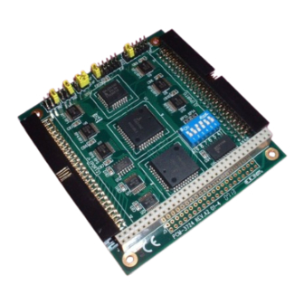
You may want to refer to the figure below for help identifying module components. Note: Do not install or remove the PCM-3724 I/O board while the power is ON, as this may damage the plug-in board or CPU card. - Page 16 We set the PCM-3724 for a base address of Hex 300 at the factory. If you need to adjust it to some other address range, set SW1 as show below:...
- Page 17 Jumpers JP3 and JP4 select the trigger edge (rising or falling) for I/O lines PC00 and PC10, respectively. Jumpers setting appear below: If you set the PCM-3724 to trap on a rising edge, the module will gener- ate an interrupt if the I/O line (PC00 or PC10) changes from TTL LOW to TTL HIGH.
- Page 18 Interrupt mode (JP5, JP6) The PCM-3724 provides two I/O lines (PC00 and PC10) which you can use to generate hardware interrupts to the PC. Jumper JP5 controls inter- rupt line PC00, and jumper JP6 controls interrupt line PC10. The DIS set- ting for each jumper (shown in the figure below) disables the corresponding line's interrupt capability.
-
Page 19: Hardware Installation
Remove the CPU card from the chassis (if necessary) to gain access to the cards PC/104 connector. Connect connector J1 of the PCM-3724 card to the PC/104 connec- tor. Carefully align the pins with the PC/104 connector. Slide the module into the connector. The module pins may not slide all the way into the connector;... - Page 20 PCM-3724 User Manual...
- Page 21 Operation...
-
Page 22: Chapter 3 Operation
I/O racks and modules, such as those manufactured by OPTO-22, Potter Brumfield, Gordos, etc. The PCM-3724's two 50-pin male IDC connectors interface with directly to OPTO-22 racks. The PCM-3724 offers two I/O lines (PC00 and PC10) to generate hardware interrupts. PCM-3724 User Manual... -
Page 23: 8255 Mode 0 Function Definitions
• Six 8-bit ports (Port A0, B0, C0, A1, B1 and C1) • Any port can be used for input or output • Outputs are latched, whereas input are not latched • The PCM-3724 requires ten I/O ports, identified below: I/O Port Assignments Location... -
Page 24: 8255 Data Registers
3.2.3 8255 Data Registers The PCM-3724's I/O ports (BASE+0 to 2 and BASE+4 to 6) directly map to the 8255 ports. Bits assignments for each I/O port appear below: BASE+0 8255 Port A0 (read/write) Value PA07 PA06 PA05 PA04 PA03... -
Page 25: 8255 Mode Registers
3.2.4 8255 Mode Registers BASE+3 8255 Mode Register Port A0, B0, C0 (write) Value Where: PB0: 0= Port B0 as output 1=Port B0 as input PC0: 0= Port C0 as output 1=Port C0 as input PA0: 0= Port A0 as output 1=Port A0 as input BASE+7 8255 Mode Register Port A1, B1, C1 (write) Value... -
Page 26: Gate Control
3.2.5 Gate control Six 74HCT245 chips (one for each port) buffer the PCM-3724's I/O lines to increase driving capacity. Because the 74HCT245 is a bidirectional, tri-state line buffer, you need to set two additional I/O ports (BASE+8 and 9) to control the direction of data flow. - Page 27 Address assignments for the buffer direction register (BASE+8) and gate control register (BASE+9) appear below: BASE+8 Buffer Direction (write) Value Where: DA0: 0=Port A0 as output 1=Port A0 as input DB0: 0=Port B0 as output 1=Port B0 as input DC0: 0=Port C0 as output 1=Port C0 as input DA1:...
-
Page 28: Interrupt Functions
3.3 Interrupt Functions 3.3.1 Introduction The PCM-3724 offers two I/O lines, PC00 and PC10, which you can use to generate a hardware interrupt to the CPU. Interrupts are edge-trig- gered. Note: Since the PCM-3724's digital input data are not latched, the module provides no "first event"... - Page 29 Free Manuals Download Website h p://myh66.com h p://usermanuals.us h p://www.somanuals.com h p://www.4manuals.cc h p://www.manual-lib.com h p://www.404manual.com h p://www.luxmanual.com h p://aubethermostatmanual.com Golf course search by state h p://golfingnear.com Email search by domain h p://emailbydomain.com Auto manuals search h p://auto.somanuals.com TV manuals search h p://tv.somanuals.com...
Need help?
Do you have a question about the PCM-3724 and is the answer not in the manual?
Questions and answers