Table of Contents
Advertisement
Quick Links
Advantech PCM-3353F-L0A3
AMD LX800 PC/104-Plus SBC
A l l t r a d e m a r k s , b r a n d n a m e s , a n d b r a n d s a p p e a r i n g h e r e i n a r e t h e p r o p e r t y o f t h e i r r e s p e c t i v e o w n e r s .
• C r i t i c a l a n d e x p e d i t e d s e r v i c e s
• I n s t o c k / R e a d y - t o - s h i p
Artisan Scientific Corporation dba Artisan Technology Group is not an affiliate, representative, or authorized distributor for any manufacturer listed herein.
$
1795
.00
In Stock
Qty Available: 1
New From Surplus Stock
Buy Today!
https://www.artisantg.com/72918-1
• We b u y y o u r e x c e s s , u n d e r u t i l i z e d , a n d i d l e e q u i p me n t
• F u l l - s e r v i c e , i n d e p e n d e n t r e p a i r c e n t e r
Advertisement
Table of Contents

Related Manuals for Advantech PCM-3353F-L0A3


Summary of Contents for Advantech PCM-3353F-L0A3
- Page 1 Advantech PCM-3353F-L0A3 AMD LX800 PC/104-Plus SBC 1795 In Stock Qty Available: 1 New From Surplus Stock Buy Today! https://www.artisantg.com/72918-1 A l l t r a d e m a r k s , b r a n d n a m e s , a n d b r a n d s a p p e a r i n g h e r e i n a r e t h e p r o p e r t y o f t h e i r r e s p e c t i v e o w n e r s .
- Page 2 User Manual PCM-3353 PC/104+ SBC w/AMD LX800/ LX600, VGA, LCD, LAN, USB2.0 and CF...
- Page 3 No part of this manual may be reproduced, copied, translated or transmitted in any form or by any means without the prior written permission of Advantech Co., Ltd. Information provided in this manual is intended to be accurate and reliable. How- ever, Advantech Co., Ltd.
-
Page 4: Declaration Of Conformity
Discard used batteries according to the manufacturer’s instructions. Technical Support and Assistance Visit the Advantech web site at http://support.advantech.com where you can find the latest information about the product. Contact your distributor, sales representative, or Advantech's customer service center for technical support if you need additional assistance. Please have the following information ready before you call: –... -
Page 5: Packing List
Packing List Before setting up the system, check that the items listed below are included and in good condition. If any item does not accord with the table, please contact your dealer immediately. 1 x PCM-3353 SBC 1 x Power cable 1 x Audio cable (p/n:1700000918) 1 x COM cable... -
Page 6: Table Of Contents
Contents Chapter General Information ......1 Introduction ....................2 Features ....................2 Specifications .................... 2 1.3.1 Standard PC/104 Biscuit SBC Functions........2 1.3.2 VGA/LVDS Interface ..............3 1.3.3 Ethernet Interface ................. 3 1.3.4 Audio Function ................3 1.3.5 OS support..................3 1.3.6 Mechanical and Environmental............. - Page 7 Entering Setup ..................14 Figure 3.1 Award BIOS setup initial screen....... 14 Standard CMOS Setup ................15 Figure 3.2 Standard CMOS setup screen ......... 15 Advanced BIOS Features ............... 16 Figure 3.3 Advanced BIOS features screen ......16 Advanced Chipset Features..............18 Figure 3.4 Advanced chipset features screen ......
- Page 8 System I/O Ports ..................42 Table B.1: System I/O Ports ............42 1st MB Memory Map ................42 Table B.2: 1st MB Memory Map ..........42 DMA Channel Assignments ..............43 Table B.3: DMA Channel Assignments........43 Interrupt Assignments ................43 Table B.4: Interrupt Assignments..........
- Page 9 PCM-3353 User Manual viii...
-
Page 10: Chapter 1 General Information
Chapter General Information This chapter gives background information on the PCM-3353. -
Page 11: Introduction
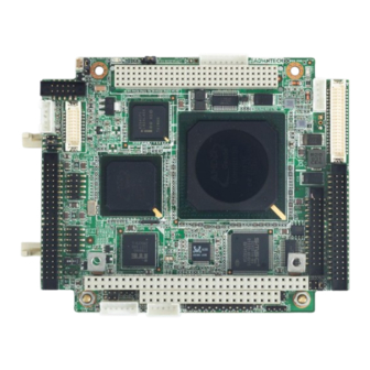
Introduction The PCM-3353 is a fanless, best-cost, performance PC/104+ SBC (Single Board Computer) geared to satisfy the needs for various industrial computing equipment. PCM-3353 is ideal for communication, gaming and medical applications that require flat panel support using digital displays with TTL and LVDS interfaces and single Ethernet ports. -
Page 12: Vga/Lvds Interface
OS support This board supports Win XP, Win CE and Win XPe. For further information about OS support in your PCM-3353, visit the following web resource Advantech: website: www.advantech.com or please contact tech- nical support center 1.3.6 Mechanical and Environmental Dimensions: 96 x 115 mm (3.77"x 4.05"), Mechanical Drawing (dxf file) is avail-... -
Page 13: Board Layout: Dimensions
Board Layout: Dimensions Figure 1.1 Board layout: dimensions (component side) Figure 1.2 Board layout: dimensions (solder side) PCM-3353 User Manual... -
Page 14: Chapter 2 Installation
Chapter Installation This chapter explains the setup procedures of the PCM-3353 hard- ware, including instructions on setting jumpers and connecting peripherals, switches and indica- tors. Be sure to read all safety pre- cautions before you begin the installation procedure. -
Page 15: Jumpers
Jumpers The PCM-3353 has a number of jumpers that allow you to configure your system to suit your application. The table below lists the functions of the various jumpers. Table 2.1: Jumper/Switch Setting Clear CMOS PCI VI/O Power Selector CN39 COM2 Setting CF Master / Slave Selector LVDS Power Selector... -
Page 16: Locating Connectors
Locating Connectors Figure 2.1 Connectors (component side) Figure 2.2 Connectors (solder side) PCM-3353 User Manual... -
Page 17: Setting Jumpers
Setting Jumpers You may configure your card to match the needs of your application by setting jump- ers. A jumper is a metal bridge used to close an electric circuit. It consists of two metal pins and a small metal clip (often protected by a plastic cover) that slides over the pins to connect them. -
Page 18: Ide, Cdrom Hard Drive Connector (Cn11)
IDE, CDROM Hard Drive Connector (CN11) The board provides 1 IDE channel which you can attach up to two Enhanced Inte- grated Drive Electronics hard disk drives or CDROM to the board’s internal controller. Its IDE controller uses a PCI interface. This advanced IDE controller supports faster data transfer, PIO mode 3, mode 4 and up to UDMA 33/66. -
Page 19: Power Connectors (Cn38)
2.10 Power Connectors (CN38) 2.10.1 Main Power Connector, +5 V, +12 V (CN38) Supplies main power +5 V to the PCM-3353, and to devices that require +12 V. 2.10.2 Power Reset Button Momentarily pressing the reset button will activate a reset. The switch should be rated for 10 mA, 5 V. -
Page 20: Lvds Tft Lcd Connector (Cn42)
2.13.3 LVDS TFT LCD Connector (CN42) Four PCM-3353 series, the board supports 1 channel 18-bit LVDS LCD panel dis- plays. 2.14 Ethernet Configuration The board is equipped with one high performance 32-bit PCI-bus Ethernet interface which are fully compliant with IEEE 802.3U 10/100Mbps standards. They are sup- ported by all major network operating systems. - Page 21 PCM-3353 User Manual...
-
Page 22: Chapter 3 Award Bios Setup
Chapter Award BIOS Setup... -
Page 23: Introduction
Turn on the computer and check for the ìpatch codeî. If there is a number assigned to the patch code, it means that the BIOS supports your CPU. If there is no number assigned to the patch code, please contact Advantechís appli- cations engineer to obtain an up-to-date patch code file. This will ensure that your CPUís system status is valid. -
Page 24: Standard Cmos Setup
Standard CMOS Setup Choose the “Standard CMOS Features” option from the “Initial Setup Screen” menu, and the screen below will be displayed. This menu allows users to configure system components such as date, time, hard disk drive, video, Halt On, display, and memory. Figure 3.2 Standard CMOS setup screen Date The date format is <Weekday>, <Month>, <Day>, <Year>. -
Page 25: Advanced Bios Features
Advanced BIOS Features The “Advanced BIOS Features” screen appears when choosing the “Advanced BIOS Features” item from the ìInitial Setup Screenî menu. It allows the user to configure the board according to his particular requirements. Below are some major items that are provided in the Advanced BIOS Features screen. - Page 26 Disabled Do not assign this boot priority. Boot Up NumLock Status [On] When enabled, the keyboard keypad boots up in number mode. When disabled, the keypad boots up in cursor control mode (arrow mode). Gate A20 Option [Fast] This item enables users to switch A20 control by port 92 or not. Typematic Rate Setting [Disabled] This item enables users to enable or disable typematic action.
-
Page 27: Advanced Chipset Features
Small Logo (EPA) Show [Disabled] Show EPA logo during system post stage. Cyrix 6X86/MII CPUID [Enabled] This item allows user to control BIOS enabled or disabled CPUID for CPU Cyrix/ MII. Advanced Chipset Features Figure 3.4 Advanced chipset features screen Note! This Advanced Chipset Features screen controls the configuration of the board’s chipset for fine-tuning system performance. -
Page 28: Integrated Peripherals
Memory Hole At 15 M-16 M [Disabled] This item reserves 15 MB-16 MB memory address space to ISA expansion cards that specifically require the setting. Memory from 15 MB-16 MB will be unavailable to the system because only expansion cards can access memory in this area. - Page 29 IDE Primary Slave UDMA [Auto] This item allows adjustment of primary slave IDE mode or type for modification purposes. Suggested BIOS default value is "Auto". IDE DMA transfer access [Enabled] This item allows adjustment of IDE DMA mode. Enabling increases IDE Data transfer speed.
-
Page 30: Power Management Setup
Parallel Port Mode [Standard] This item allows user to change parallel port mode. User can choose "SPP", "EPP", "ECP" and "ECP+EPP". SPP (Standard Parallel Port). ECP (Extended Capabilities Port). EPP (Enhanced Parallel Port). Suggested BIOS default value is "Normal". ECP Mode Use DMA [3] This selection is available only if you select ìECPî... -
Page 31: Pnp/Pci Configurations
Max. Power Saving Maximum power management., Suspend Mode = 1 min., and HDD Power Down = 1 min. User Defined (Default) Allows you to set each mode individually. When not disabled, each of the ranges are from 1 min. to 1 hr. except for HDD Power Down which ranges from 1 min. -
Page 32: Pc Health Status
Resources Controlled By [Auto (ESCD)] – IRQ Resources This item allows you respectively to assign interrupt types for IRQ-3, 4, 5, 7, 9,10, 11,12, 14, and 15. – Memory Resources This item allows you respectively to assign memory blocks from N/A to DC00. -
Page 33: Load Optimized Defaults
3.10 Load Optimized Defaults Figure 3.9 Load optimized defaults screen The PCM-3353 automatically configures all setup items to optimal settings when you select this option. Optimal Defaults are designed for maximum system performance, but may not work best for all computer applications. In particular, do not use the Opti- mal Defaults if your computer is experiencing system configuration problems. -
Page 34: Save And Exit Setup
To change the password: Choose the “Set Password” option from the “Initial Setup Screen” menu and press <Enter>. The screen will display the following message. Press <Enter>. If the CMOS is good or if this option has been used to change the default pass- word, the user is asked for the password stored in the CMOS. -
Page 35: Exit Without Saving
3.13 Exit without Saving Figure 3.12 Exit without saving screen Selecting this option and pressing <Enter> lets you exit the setup program without recording any new values or changing old ones. PCM-3353 User Manual... -
Page 36: Pin Assignments
Appendix Pin Assignments This appendix contains informa- tion of a detailed or specialized nature. -
Page 37: Jumper And Connector Tables
Jumper and Connector Tables Table A.1: SW1, CF Master / Slave Selector Part Number 1600000071 Footprint JH2X1V-2M PIN HEADER 2*1P Description 180D (M)SQUARE 2.0mm Setting Function (1 - 2) Master (default) (2 - 3) Slave Table A.2: J3, Clear CMOS Part Number 1653003101 Footprint... - Page 38 Table A.4: J5, PCI VI/O POWER Part Number 1653003101 Footprint JH3X1V-2M PIN HEADER 3*1P Description 180D (M)SQUARE 2.0mm Setting Function (1 - 2) With +5 V (2 - 3) With +3.3 V (defualt) Table A.5: J6, LVDS Power Selector Part Number 1653003260 Footprint HD_3x2P_79...
- Page 39 NONE NONE CLK+ CLK- +12 V/+5 V/+3.3 V +12 V/+5 V/+3.3 V +12 V/+5 V/+3.3 V +12 V/+5 V/+3.3 V Table A.7: CN38, Power Input Part Number 1655308020 Footprint PWR-B4PV Description PIN HEADER DIP 8*1P 180D(M) 2.00mm Pin Name Signal Type Signal Level +5 V +5 V...
- Page 40 +3.3 V +3.3 V TV-CLK CLK48M +3.3 V +3.3 V +3.3 V +3.3 V +3.3 V +3.3 V +3.3 V +3.3 V +3.3 V +3.3 V +3.3 V +3.3 V +3.3 V +3.3 V +3.3 V +3.3 V +3.3 V +3.3 V +3.3 V +3.3 V...
- Page 41 ENABKL +3.3V +3.3V Table A.10: CN6, SMBus Part Number 1653002101 Footprint JH2X1V-2M Description PIN HEADER 2*1P 180D (M)SQUARE 2.0mm Pin Name Signal Type Signal Level SMB-CLK +3 V SMB-DAT +3 V Table A.11: CN32, Reset / Buzzer pin header Part Number 1653002201 Footprint WHL2V-2M...
- Page 42 GPIO0 +5 V GPIO1 +5 V GPIO2 +5 V GPIO3 +5 V Table A.13: CN37, GPIO2 Part Number 1653010100 Footprint JH5X2S-2M Description PIN HEADER SMD 5*1P 180D(M) 2.54mm Pin Name Signal Type Signal Level GPIO4 +5 V GPIO5 +5 V GPIO6 +5 V GPIO7...
- Page 43 +5 V +5 V +5 V DREQ +5 V IOW# +5 V IOR# +5 V IORDY +5 V CSEL# +5 V DACK# +5 V IRQ14 +5 V +5 V D66DET# +5 V +5 V +5 V CS#1 +5 V CS#3 +5 V ASP# +5 V...
- Page 44 Table A.16: CN15, USB1/2 Part Number 1653005260 Footprint JH5X2S-2M Description PIN HEADER 5*2P 180D(M) 2.0mm SMD IDIOT-PROOF Pin Name Signal Type Signal Level +5 V +5 V +5 V +5 V Table A.17: CN17, USB3/4 Part Number 1653005260 Footprint JH5X2S-2M Description PIN HEADER 5*2P 180D(M) 2.0mm SMD IDIOT-PROOF Pin Name...
- Page 45 Table A.18: CN30, COM1/2/3/4 Part Number 1653220260 Footprint BH20X2SV-2.00mm Description Pin Name Signal Type Signal Level DCD#1 -3 ~ -12 V, +3 ~ +12 V DSR#1 -3 ~ -12 V, +3 ~ +12 V RXD1 -3 ~ -12 V, +3 ~ +12 V RTS#1 -3 ~ -12 V, +3 ~ +12 V TXD1...
- Page 46 Table A.19: CN19, Print Port Part Number 1653213260 Footprint BH13x2SV-2.00 Description BOX HEADER SMD 13*2P 180D(M) 2.0mm Pin Name Signal Type Signal Level STB# +5 V AFD# +5 V +5 V ERR# +5 V +5 V INIT# +5 V +5 V SLIN# +5 V +5 V...
- Page 47 Table A.20: CN20, RS422/485 Part Number 1653004101 Footprint JH4X1V-2M Description PIN HEADER 4*1P 180D(M) SQUARE 2.0mm Pin Name Signal Type Signal Level 422-RXD- +5 V 422-RXD+ +5 V 485-422-TXD+ +5 V 485-422-TXD- +5 V Table A.21: CN35, AUDIO-OUT Part Number 1655303120 Footprint WHL3V-2M...
- Page 48 Table A.23: CN23, ISA -5V & -12V Input Part Number 1653003101 Footprint JH3X1V-2M Description PIN HEADER 3*1P 180D (M)SQUARE 2.0 mm Pin Name Signal Type Signal Level -12 V -12 V -5 V -5 V Table A.24: CN26, LAN1 Part Number 1653205260 Footprint BH5X2SV...
- Page 49 Table A.25: CN18, KB/MS Part Number 1655306020 Footprint BH5X2SV Description BOX HEADER DIP 6*1 180D (M) 2.0 mm Pin Name Signal Type Signal Level KB-CLK +5 V KB-DATA +5 V MS-CLK +5 V +5 V +5 V MS-DATA +5 V Table A.26: CN40, DDR RAM SOCKET Part Number 1651000051...
-
Page 50: System Assignments
Appendix System Assignments This appendix contains informa- tion of a detailed nature. -
Page 51: System I/O Ports
System I/O Ports Table B.1: System I/O Ports Addr. range (Hex) Device 000-01F DMA controller 020-021 Interrupt controller 1, master 040-05F 8254 timer 060-06F 8042 (keyboard controller) 070-07F Real-time clock, non-maskable interrupt (NMI) mask 080-09F DMA page register 0A0-0BF Interrupt controller 2 0C0-0DF DMA controller Clear math co-processor... -
Page 52: Dma Channel Assignments
Table B.2: 1st MB Memory Map Addr. range (Hex) Device * If Ethernet boot ROM is disabled (Ethernet ROM occupies about 16 KB) * E0000 - EFFFF is reserved for BIOS POST DMA Channel Assignments Table B.3: DMA Channel Assignments Channel Function Available... - Page 53 PCM-3353 User Manual...
-
Page 54: Appendix C Watchdog Timer Sample Code
Appendix Watchdog Timer Sample Code... -
Page 55: Watchdog Function
Watchdog Function ;The SCH3114 Runtime base I/O address is 800h ;Setting WatchDog time value location at offset 66h ;If set value "0", it is mean disable WatchDog function. Superio_GPIO_Port = 800h mov dx,Superio_GPIO_Port + 66h mov al,00h out dx,al .model small .486p .stack 256 .data... - Page 56 ;==================================================== mov dx,SCH3114_IO + 68h mov al,01h out dx,al .exit PCM-3353 User Manual...
- Page 57 PCM-3353 User Manual...
-
Page 58: Appendix Dgpio Sample Code
Appendix GPIO Sample Code... -
Page 59: Gpio Sample Code
Output_Reg EQU 01h Inversion_Reg EQU 02h Configure_Reg EQU 03h Advantech_Str db 'Advantech Company Copyright (C) 2005 Design by Dun- can',0AH,0Dh,'$' Advantech_Str db 'Advantech Company Copyright (C) 2005 Design by Dun- can, Modify by Steven',0AH,0Dh,'$' GX3_Fun_Str db 'Check Philip GPIO function.',0Ah,0Dh,'$' Note1_Str db 'Test Method: GPIO 0 connect to GPIO 1.',0Ah,0Dh,'$'... - Page 60 db 'Fifth GPIO Chip Test Fail !! ',0Ah,0Dh,'$' db 'Sixth GPIO Chip Test Fail !! ',0Ah,0Dh,'$' db 'Seventh GPIO Chip Test Fail !!',0Ah,0Dh,'$' db 'Eighth GPIO Chip Test Fail !! ',0Ah,0Dh,'$' Error_Str1 db 'Error !! The system has no GPIO Chip or no support INT15 hook! ',0Ah,0Dh,'$' ;=============================================================== ====...
- Page 61 ;=============================================================== ==== ;=============================================================== ==== Get GPIO Config ; Input: ax=5E87h bh=01h cl= n ; n means which group of GPIO you want to get ; output: ax=5E78 ;function success, other value means function fail bl= the n group of gpio config bit 0 = gpio 0 , 0 =>...
- Page 62 bl= the n group of gpio status bit 0 = gpio 0 , 0 => Low; 1 => High bit 1 = gpio 1 , 0 => Low; 1 => High ..bit 7 = gpio 7 , 0 => Low; 1 => High ;=============================================================== ==== ;===============================================================...
- Page 63 ;3. Check GPI 1,3,5,7 value ;restore NO. of GPIO chip push ;save NO. of GPIO chip ax,5e87h bx,03FFh ;restore NO. of GPIO chip push ;save NO. of GPIO chip al,Fail_lenght dx, Fail_Str dx,ax bl,00 test_result ;4. Set GPIO 0,2,4,6 Output differential ;restore NO.
- Page 64 test_fail ;4.Set GPIO 1,3,5,7 as output,GPIO 0,2,4,6 as input push ax,5e87h bx,0255h ;4. Set GPIO 1,3,5,7 Output High ;restore NO. of GPIO chip push ;save NO. of GPIO chip ax,5e87h bx,04ffh ;6. Check GPIO 0,2,4,6 value ;restore NO. of GPIO chip push ;save NO.
- Page 65 ;restore NO. of GPIO chip push ;save NO. of GPIO chip al,Fail_lenght dx, Fail_Str dx,ax bl,33h test_result ;restore NO. of GPIO chip push ;save NO. of GPIO chip al,Success_lenght dx, Success1_Str dx,ax ;Do Second PCA9554 test ;1.Set GPIO 0,2,4,6 as output, GPI 1,3,5,7 as input test_result: ah,09h next_test...
- Page 66 NEWIODELAY call CT_Chk_SMBus_Ready pop ax mov dl,03h dx,al ;Index NEWIODELAY NEWIODELAY mov dl,02h mov al,48h dx,al ;Read data NEWIODELAY NEWIODELAY mov cx, 100h newiodelay loop short @B call CT_Chk_SMBus_Ready mov dl,05 al,dx ;Data0 NEWIODELAY NEWIODELAY Ct_I2CReadByteEndp ;============================================================== ;Input : CL - register index CH - device ID AL - Value to write ;Output: none...
- Page 67 call Delay5ms call Delay5ms call CT_Chk_SMBus_Ready pop ax mov dl,03h dx,al ;Index call Delay5ms call Delay5ms pop ax mov dl,05 dx,al ;Data0 call Delay5ms call Delay5ms mov dl,02h mov al,48h dx,al ;write data call Delay5ms call Delay5ms mov cx, 100h newiodelay loop short @B call...
- Page 68 and al, NOT 40H;mask INUSE bit al,al ;status OK ? short Clear_final test al,04h ;device error short SMBus_Err loop short Chk_I2c_OK ;SMbus error due to timeout SMBus_Err: Clear_final: CT_Chk_SMBus_ReadyEndp ;;=============================================================== Delay5msprocnear push cx mov cx, 1000 NEWIODELAY loop short @B pop cx Delay5ms ENDP...
- Page 69 ;=============================================================== ==== PCM-3353 User Manual...
- Page 70 PCM-3353 User Manual...
- Page 71 No part of this publication may be reproduced in any form or by any means, electronic, photocopying, recording or otherwise, without prior written permis- sion of the publisher. All brand and product names are trademarks or registered trademarks of their respective companies. © Advantech Co., Ltd. 2010...
Need help?
Do you have a question about the PCM-3353F-L0A3 and is the answer not in the manual?
Questions and answers