Table of Contents
Advertisement
Quick Links
Advertisement
Table of Contents

Related Manuals for Advantech PCM-3718H


Summary of Contents for Advantech PCM-3718H
- Page 3 Contents CHAPTER 1: General Information ......1 1.1 Introduction ................2 1.2 Features ................. 2 1.3 Specifications ................. 3 1.4 Locating Components ............5 1.5 Daughterboards ..............6 1.6 Software Support..............7 1.7 Block Diagram ............... 8 CHAPTER 2: Installation ........9 2.1 Initial Inspection ..............
-
Page 4: Table Of Contents
7.3 Counter Operating Modes............ 48 7.4 Counter Operations .............. 50 7.5 Counter Applications............51 CHAPTER 8: Direct Memory Access Operation 53 8.1 Using DMA Transfer with the PCM-3718H/3718HG ... 54 CHAPTER 9: Calibration ........57 9.1 VR Assignment ..............58 9.2 A/D Calibration..............58... - Page 6 A/D conversion with DMA and individual channel gains. The PCM-3718H/3718HG is an advanced new version of our popular PCL-818 multifunction data acquisition card series. A custom 160- pin ASIC chip integrates the functions of a full-size DAS card. This chip gives you maximum accuracy and reliability, along with minimum cost, size and power consumption.
- Page 7 PCM-3718HG Bipolar: ±10, ±5, ±1, ±0.5, ±0.1, ±0.05, ±0.01, ±0.005 Unipolar: 0 ~ 10, 0 ~ 1, 0 ~ 0.1, 0 ~ 0.01 • Maximum data throughput PCM-3718H: 100 kHz PCM-3718HG: (variable, depending on PGIA settling time) Gain Speed 0.5, 1...
- Page 8 • Operating temperature: 0 to +60°C (refer to IEC 68-2-1, 2) • Storage temperature: -20 to +70°C • Operating humidity: 5 to 95% non-condensing (refer to IEC 68-2-3) • MTBF: over 235,346 hrs @ 25°C, ground, fix environment PCM-3718H/3718HG User's Manual...
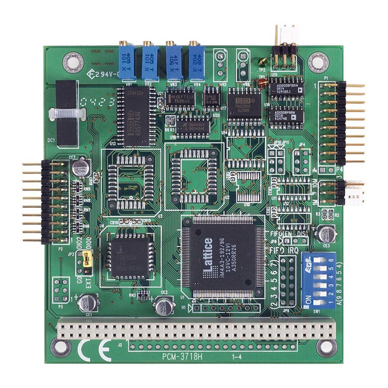
- Page 9 JP 2 V R 1 V R 2 V R 3 JP 1 S W 1 JP 3 Connectors, switches and VR locations Label Function PC-bus connector DMA level (1 or 3) and time base (1MHz or 10MHz) Differential or single-ended inputs DIO0 or external input Analog input Digital input/output connector...
- Page 10 We offer a wide variety of optional daughterboards to help you get the most from your PCM-3718H/3718HG. You will need the PCLD- 780/880 Screw-terminal Board or the PCLD-8115 Wiring Terminal Board to make connections. This analog input-signal conditioning board multiplexes 16 differen- tial inputs to one A/D input channel.
-
Page 11: Features
The PCM-3718H/3718HG comes with a powerful and easy-to-use software driver. This driver makes application programming much easier, especially when you use sophisticated features like interrupt or DMA data transfer. For building up a high performance Human Machine Interface (HMI), you may need other supporting software beside our included driver to the PCM-3718/3718HG. - Page 12 PC BUS PCM-3718H/3718HG User's Manual...
-
Page 14: Specifications
It should be free of marks and scratches and in perfect order on receipt. As you unpack the PCM-3718H/3718HG, check it for signs of shipping damages (damaged box, scratches, dents, etc.). If it is damaged or fails to meet specifications, notify our service department or your local sales representative immediately. - Page 15 Hex 000 to Hex 3F0. Other devices in your system can use some of these addresses. We set the PCM-3718H/3718HG for a base address of Hex 300 at the factory. If you need to adjust it to other address ranges, set SW1 by...
- Page 16 The PCM-3718H/3718HG supports DMA data transfer. The bottom pins of JP1 provide selection of DMA channel 1 or 3, as shown in the following figure. Channel 1 Channel 3 (default) 1 0M 1 0M D M 1 D M 3...
- Page 17 Digital I/O line DIO 0 (default) DIO0 DIO0 The PCM-3718H/3718HG has two on-board 20-pin flat-cable connectors (insulation displacement, mass termination). The figure on page 5 shows locations of both connectors. Refer to the table below for abbreviations of the pin assignment.
- Page 18 D IO 1 0 D IO 11 D IO 1 2 D IO 1 3 D IO 1 4 D IO 1 5 D .G N D D .G N D + 5 V + 1 2V PCM-3718H/3718HG User's Manual...
- Page 19 4. Remove the CPU card from the chassis (if necessary) to gain access to the card’s PC/104 connector. 5. Connect the connector J1 of the PCM-3718H/3718HG to the PC/ 104 connector. Carefully align the pins to the PC/104 connector. Slide the module into the connector. The module pins may not slide all the way into the connector;...
- Page 20 The PCM-3718H/3718HG includes a CD-ROM with utility software. The CD-ROM contains: 1. A comprehensive I/O driver for A/D and digital I/O applications. This driver lets you use standard functions, written in common programming languages, to operate the PCM-3718H/3718HG. You do not need to perform detailed register programming. The driver supports the following languages: Microsoft Visual Basic, Visual C++, Borland C++, C++ Builder and Delphi.
- Page 22 PC and other hardware. This chapter provides information on signal connections for different types of data acquisition applications. The PCM-3718H/3718HG supports either 16 single-ended or eight differential analog inputs. Jumper JP2 selects the input channel configuration. The major difference between single-ended and differential input connections is the number of signal wires per input channel.
- Page 23 A.GND If the signal source has one side connected to a local ground, the signal source ground and the PCM-3718H/3718HG ground will not be at exactly the same voltage, as they are connected through the ground return of the equipment and building wiring. The difference between the ground voltages forms a common-mode voltage.
-
Page 24: Daughterboards
You can expand any or all of the PCM-3718H/3718HG’s A/D input channels by using the multiplexing daughterboards. Most daughter- boards are connected directly to the module’s 20-pin connectors. You may require the PCLD-8115 Screw-terminal Board for connections. The PCLD-789 Amplifier and Multiplexer multiplexes 16 differential inputs to one A/D input channel. -
Page 25: Chapter 3: Signal Connections
To receive an OPEN/SHORT signal from a switch or relay, add a pull- up resistor to ensure that the input is held at a high level when the contacts are open. See the figure below: 4.7K D.GND Chapter 3 Signal Connections... - Page 26 PCM-3718H/3718HG User's Manual...
- Page 28 The key to programming the PCM-3718H/3718HG is to understand the function of the card’s 16 registers. The PCM-3718H/3718HG requires 16 consecutive addresses in the PC’s I/O space. Each address corresponds to a card register. The address of each register is specified as an offset from the card’s base address.
-
Page 29: Chapter 4: Register Structure And Format
Two read-only registers at BASE+0 and BASE+1 hold A/D conversion data. The 12 bits of data from the A/D conversion are stored in BASE+1 bit 7 to bit 0 and BASE+0 bit 7 to bit 4. BASE+0 bits 3 to 0 store the source A/D channel number. - Page 30 0 to 3 of BASE+1. BASE+1 (write only) - A/D range control code Value N/A Input Range(V) Unipolar/Bipolar Range Code ±5 ±2.5 ±1.25 ±0.625 0 to 10 0 to 5 0 to 2.5 0 to 1.25 ±10 PCM-3718H/3718HG User's Manual...
- Page 31 Input Range(V) Unipolar/Bipolar Range Code ±5 ±0.5 ±0.05 ±0.005 0 to 10 0 to 1 0 to 0.1 0 to 0.01 ±10 ±1 ±0.1 ±0.01 Read/write register BASE+2 controls multiplexer (MUX) scanning. The high nibble provides the stop scan channel number, and the low nibble provides the start scan channel number.
- Page 32 Do not forget to reset the MUX start and stop channels to the correct values after your range setting. The PCM-3718H/3718HG offers two 8-bit digital input/output channels. These I/O channels use the input or output ports at address- es Base+3 and BASE+11.
- Page 33 BASE+3 (read port) -DIO low byte Value DIO7 DIO6 DIO5 DIO4 DIO3 DIO2 DIO1 DIO0 BASE+3 (write port) DIO low byte Value DIO7 DIO6 DIO5 DIO4 DIO3 DIO2 DIO1 DIO0 BASE+11 (read port) - DIO high byte Value DIO15 DIO14 DIO13 DIO12 DIO11 DIO10 DIO9 DIO8 BASE+11 (write port) - DIO high byte Value DIO15 DIO14 DIO13 DIO12 DIO11 DIO10 DIO9 DIO8 Read-only register BASE+8 provides information on the A/D configu-...
-
Page 34: Chapter 5: A/D Conversion
Your software should therefore wait for the signal INT = 1 before it reads the conversion data. It should then clear the INT bit by writing any value to the A/D status register BASE+8. PCM-3718H/3718HG User's Manual... - Page 35 Disables the generation of interrupts. No interrupt signal will be sent to the PC bus. Enables the generation of interrupts. If DMAE = 0, the PCM-3718H/3718HG will generate an interrupt when it completes an A/D conversion. Use this setting for interrupt driven data transfer.
- Page 36 Enables DMA transfer. Each A/D conversion initiates two successive DMA request signals. These signals cause the 8237 DMA controller to transfer two bytes of conversion data from the PCM-3718H/3718HG to memory. Note: You must program the PC’s 8237 DMA controller as the DMA page register before you set DMAE to1.
- Page 37 These four registers located at addresses BASE+12, BASE+13, BASE+14 and BASE+15 are used for the Intel 8254 programmable pacer. Please refer to Chapter 7 Programmable Pacer or 8254 product literature for detailed application information. Chapter 4 Register Structure and Format...
- Page 38 PCM-3718H/3718HG User's Manual...
-
Page 40: Input Range Selection
The last section gives step by step implementation guidelines for A/D operations. Since the PCM-3718H/3718HG uses 12-bit A/D conversions, a single 8-bit register will not accommodate all the data. The PCM-3718H/ 3718HG therefore stores A/D data in two registers located at addresses BASE+0 and BASE+1. - Page 41 BASE+2. Bits D0 to D3 hold the starting channel number, and positions D4 to D7 hold the stop scan channel number. When you set the PCM-3718H/3718HG for eight differential input channels, set bits CH3 and CL3 to zero.
- Page 42 If you require only one A/D input channel, you should set the high and low scan limits to the same value. If you specify a range of input channels, the PCM-3718H/3718HG automatically performs an A/D conversion on each channel in the range, beginning with the start channel.
-
Page 43: A/D Data Transfer
EOC signal generates an interrupt, and the interrupt handler routine performs the transfer. You must specify the interrupt control bit and the interrupt level selection bits in the PCM-3718H/3718HG control register (BASE+9) before using the Chapter 5 A/D Conversion... - Page 44 DMA level (JP1), the DMA enable bit control register (BASE+9) and the registers in the 8237 DMA controller. We recommend that you use the PCM-3718H/3718HG driver to perform DMA operations. See Chapter 8 for more Information on the 8237 DMA controller and PCM-3718H/3718HG DMA opera- tions.
-
Page 46: Chapter 6: Digital Input/Output
Value DIO15 DIO14 DIO13 DIO12 DIO11 DIO10 DIO9 DIO8 BASE+11 (wirte port) - DIO high byte Value DIO15 DIO14 DIO13 DIO12 DIO11 DIO10 DIO9 DIO8 Using the PCM-3718H/3718HG’s input and output functions is fairly straightforward. Page 20 shows some ideas for digital signal connec- tions. - Page 48 2 to 65535. Version 2 of the 8254 has a maximum input clock frequency of 10 MHz. The PCM-3718H/3718HG provides 1 MHz and 10 MHz input frequencies to the 8254 from an on-board crystal oscillator. Jumper JP1 controls the input frequency. See page 12 for more information.
-
Page 49: Chapter 7: Programmable Pacer
The 8254 programmable interval timer uses four registers at addresses BASE+12, BASE+13, BASE+14 and BASE+15. Register functions are listed below: Register Function BASE+12 Counter 0 read/write BASE+13 Counter 1 read/write BASE+14 Counter 2 read/write BASE+15 Counter control word Since the 8254 counter uses a 16-bit structure, each section of read/ write data is split into a least significant byte (LSB) and most significant byte (MSB). - Page 50 Decimal) counting, the count can be any number from 0 to 9999. If you set both SC1 and SC0 bits to 1, the counter control register is in read-back command mode. The control register data format becomes: BASE+15 - 8254 control, read-back mode Value 1 PCM-3718H/3718HG User's Manual...
-
Page 51: Counter Operations
CNT = 0 Latch count of selected counter(s). STA = 0 Latch status of selected counter(s). C2, C1 & C0 Select counter for a read-back operation. C2 = 1 select Counter 2 C1 = 1 select Counter 1 C0 = 1 select Counter 0 If you set both SC1 and SC0 to 1 and STA to 0, the register selected by C2 to C0 contains a byte which shows the status of the counter. - Page 52 You can thus use the gate input to synchronize the counter. With this mode the output will remain high until you load the count register. You can also synchronize the output by software. PCM-3718H/3718HG User's Manual...
- Page 53 This mode is similar to Mode 2, except that the output will remain high until one half of the count has been completed (for even numbers), and will go low for the other half of the count. This is accomplished by decreasing the counter by two on the falling edge of each clock pulse.
- Page 54 For the counter status format please see the beginning of the chapter. Users often want to read the value of a counter without disturbing the count in progress. You can enable this function by latching the count value for the specific counter and then reading the value. PCM-3718H/3718HG User's Manual...
- Page 55 A subsequent read operation on the selected counter will retrieve the latched value. The 8254 programmable Interval timer/counter on your PCM-3718H/ 3718HG interface module is a very useful device. You can program counters 1 and 2 as pacers to generate A/D conversion trigger pulses.
- Page 56 OUTPORTB (BASE+1, 40); /* WRITE LOW BYTE OF C1*/ OUTPORTB (BASE+1, 0); /* WRITE HIGH BYTE OF C1*/ OUTPORTB (BASE+3, 0xB6); /* SET COUNTER 2 TO MODE 3*/ OUTPORTB (BASE+2, 10); /*WRITE LOW BYTE OF C2*/ OUTPORTB (BASE+2, 0); /*WRITE HIGH BYTE OF C2*/ PCM-3718H/3718HG User's Manual...
- Page 58 Direct Memory Access (DMA) improves system performance by allowing external devices to transfer information directly to or from the PC’s memory without using the CPU. The PCM-3718H/3718HG’s DMA capability significantly improves the system performance in high-speed A/D applications. The 8237 DMA controller chip on the PC system board handles the DMA operation.
-
Page 59: Chapter 8: Direct Memory Access Operation
1. When you configure your hardware, check if any PC DMA channel is available (level 1 or level 3) and set PCM-3718H/3718HG jumper JP1 accordingly. 2. If you will be using the PCM-3718H/3718HG driver for your DMA transfer programming, see the Software Drivers User’s Manual for more information. - Page 60 PCM-3718H/3718HG User's Manual...
-
Page 62: Chapter 9: Calibration
Regular calibration checks are key factors for accuracy maintenance. We provide a calibration program, CALB.EXE, in the PCM-3718H/ 3718HG’s CD-ROM to assist you in this task. The CALB.EXE makes calibration easy. It leads you through the calibration and setup procedures with a variety of prompts and graphic displays, showing you all of the correct settings and adjust- ments. - Page 63 2. Adjust VR2 until the output from the card’s A/D converter flickers between 0 and 1. 3. Connect an external DC voltage source with a value of 4094.5 LSB to A/D channel 0. 4. Adjust VR1 until the A/D reading flickers between 4094 and 4095. 5.
- Page 64 PCM-3718H/3718HG User's Manual...
- Page 66 The PCM-3718H/3718HG is supported by a powerful software utility . The appendix lists below the supporting functions (i.e., the items with the " * " mark) of the software utility for the PCM-3718H/3718HG. (For complete function descriptions of the software utility please refer to the PC-LabCard software Utility User’s Manual).
- Page 67 Func 22 Perform digital input with DMA data transfer Func 23 Get Func 22’s operational status Func 24 Stop Func 22 Func 25 Perform digital input with interrupt data transfer Func 26 Get Func 25’s operational status Func 27 Stop Func 25 *Func 28 D/O Initialization *Func 29...
- Page 68 *Func 100 Block channel scan initialization *Func 101 Perform Block channel scan with software data transfer *Func 105 Perform Block channel scan with interrupt data transfer *Func 106 Get Func 105’s status *Func 107 Stop Func 105 PCM-3718H/3718HG User's Manual...
Need help?
Do you have a question about the PCM-3718H and is the answer not in the manual?
Questions and answers