Advantech PCM-3362 User Manual
Pc/104-plus sbc with intel atom n450, vga, lcd, lan, usb2.0, sata, and on-board flash
Hide thumbs
Also See for PCM-3362:
- Startup manual (6 pages) ,
- Startup manual (6 pages) ,
- User manual (90 pages)

Related Manuals for Advantech PCM-3362


Summary of Contents for Advantech PCM-3362
- Page 1 User Manual PCM-3362 PC/104-plus SBC with ® Intel Atom™ N450, VGA, LCD, LAN, USB2.0, SATA, and on-board flash...
- Page 2 No part of this manual may be reproduced, copied, translated or transmitted in any form or by any means without the prior written permission of Advantech Co., Ltd. Information provided in this manual is intended to be accurate and reliable. How- ever, Advantech Co., Ltd.
-
Page 3: Packing List
1 x heatspreader (p/n:1960047106T001) Additional Information and Assistance Visit the Advantech web site at www.advantech.com where you can find the lat- est information about the product. Contact your distributor, sales representative, or Advantech's customer service center for technical support if you need additional assistance. Please have the... - Page 4 Caution! There is a danger of a new battery exploding if it is incorrectly installed. Do not attempt to recharge, force open, or heat the battery. Replace the battery only with the same or equivalent type recommended by the man- flatterer. Discard used batteries according to the manufacturer's instruc- tions. PCM-3362 User Manual...
-
Page 5: Table Of Contents
2.17 ATX Power in connector (CN23)............. 15 2.18 Power Connectors (CN24) ..............15 2.19 I2C Bus connector (CN25) ..............15 2.20 -12 V & -5 V power connector (CN26) ........... 15 2.21 Watchdog timer configuration ..............15 PCM-3362 User Manual... - Page 6 Figure 3.26South Bridge Configuration ........34 Exit Option ....................35 Figure 3.27Exit Option..............35 3.8.1 Save Changes and Exit .............. 35 3.8.2 Discard Changes and Exit ............36 3.8.3 Load Optimal Defaults ..............36 3.8.4 Load Fail-Safe Defaults .............. 36 PCM-3362 User Manual...
- Page 7 Heatsink Mechanical Drawings ............... 72 Figure C.3 PCM-3362N Heatsink Mechanical Drawing ..... 72 Figure C.4 PCM-3362Z/Z2 Heatsink Mech Dwg, wide temp..72 Optional Heat spreader Mechanical Drawings........73 Figure C.5 PCM-3362 optional Heatspreader Mech Drawing ..73 PCM-3362 User Manual...
- Page 8 Appendix D Watchdog Timer and GPIO sample code............ 75 Watchdog Timer sample code ..............76 GPIO sample code.................. 77 PCM-3362 User Manual viii...
-
Page 9: Chapter 1 General Information
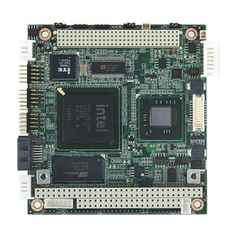
Chapter General Information This chapter gives background information on the PCM-3362. Sections include: Introduction Features Specifications Board layout and dimensions... -
Page 10: Introduction
PC/104-plus expansion interface Specifications 1.3.1 Standard PC/104-plus Biscuit SBC Functions ® CPU: Intel Atom™ N450 processor, up to 1.67 GHz System Memory: supports Double Data Rate (DDR) DDR2 667 SDRAM up to Note! PCM-3362 cannot support DDR2 533 SDRAM. PCM-3362 User Manual... -
Page 11: Vga/Lvds Interface
OS support This board supports Win7,Win XP, Win CE and Win XPe. For further information about OS support in your PCM-3362, visit the following Advantech web resource: www.advantech.com or please contact your technical sup- port center. 1.3.5 Mechanical and Environmental Dimensions: 96 x 90 mm (3.8"... -
Page 12: Board Layout: Dimensions
Operating temperature: 0 ~ 60°C (32 ~ 140°F) (operation humidity: 40°C @ 85% RH Non-Condensing) Weight: 0.85 kg (reference weight of total package) Board layout: dimensions Figure 1.1 Board layout: Dimensions (Component Side) PCM-3362 User Manual... -
Page 13: Figure 1.2 Board Layout: Dimensions (Solder Side)
Figure 1.2 Board layout: Dimensions (Solder Side) PCM-3362 User Manual... - Page 14 PCM-3362 User Manual...
-
Page 15: Chapter 2 Hardware Installation
Chapter Hardware Installation... -
Page 16: Jumpers
CN19 LAN LED Connector CN20 PS2 Keyboard/Mouse Connector CN21 GPIO Connector CN23 ATX Power In Connector CN24 Power In Connector CN25 I2C BUS connector CN26 -12 V & -5 V power connector PC104-plus Connector RTC Battery Connector PCM-3362 User Manual... -
Page 17: Locating Connectors & Block Diagram
Locating Connectors & block diagram Figure 2.1 Connectors (component side) Figure 2.2 Connectors (solder side) PCM-3362 User Manual... -
Page 18: Figure 2.3 Block Diagram
To “close” a jumper, you connect the pins with the clip. To “open” a jumper, you remove the clip. Sometimes a jumper will have three pins, labeled 1, 2 and 3. In this case you would connect either pins 1 and 2, or 2 and 3. PCM-3362 User Manual... -
Page 19: Clear Cmos (Jp1)
Warning! To avoid damaging the computer, always turn off the power supply before clearing CMOS. Table 2.3: Clear CMOS (JP1) Setting Function Normal (default) Clear CMOS 2.4.2 LVDS Panel Power Select (JP2) Table 2.4: LVDS Panel Power Select (JP2) Setting Function 3.3 V (default) PCM-3362 User Manual... -
Page 20: Com3 Rs422/Rs485 Select (Jp3)
They combine an integrated ATA Controller in a multi-chip pack- age. These products are ideal for industrial grade solid state mass storage applica- tions offering new and expanded functionality while enabling cost effective designs. PCM-3362 User Manual... -
Page 21: High Definition Audio Interface (Cn1)
-40°C to +85°C for industrial operation. High Definition Audio Interface (CN1) The PCM-3362 provides high definition audio interface. It can support high definition audio stereo by customized audio module that has codec onboard or by Advantech’s PCA-AUDIO-HDA1E module through specific cable. VGA/LCD interface connections The PCM-3362’s VGA interface can drive conventional CRT displays and is capable... -
Page 22: Buzzer Connector (Cn13)
2.11 Buzzer Connector (CN13) PCM-3362 provides one buzzer connector to connect buzzer for alert function. Buzzer, Advantech’s P/N:1750005282, can be selected to install on board. 2.12 SATA Connector (CN15) In addition to on board 2GB flash, PCM-3362 features one high performance serial ATA interfaces (up to 300 MB/s) that eases cabling to hard drives with thin and long cables while your application need more large storage capacity. -
Page 23: Gpio Connector (Cn21)
PCM-3362 provides I2C Bus connector for customer connection to I2C protocol embedded device. Advantech also provide I2C API allowing a developer to interface with an embedded system environment and transfer serial messages using the I2C protocols, allowing multiple simultaneous device control. - Page 24 PCM-3362 User Manual...
-
Page 25: Chapter 3 Ami Bios Setup
Chapter AMI BIOS Setup... -
Page 26: Figure 3.1 Setup Program Initial Screen
BIOS supports your CPU. If there is no number assigned to the patch code, please contact an Advantech application engineer to obtain an up-to-date patch code file. This will ensure that your CPU’s system status is valid. -
Page 27: Figure 3.2 Main Setup Screen
Advanced BIOS Setup option by highlighting it using the <Arrow> keys. All Advanced BIOS Setup options are described in this section. The Advanced BIOS Setup screens is shown below. The sub menus are described on the following pages. PCM-3362 User Manual... -
Page 28: Figure 3.3 Advanced Bios Features Setup Screen
This item allows you to enable or disable Intel® Hyper Threading technology. Intel® SpeedStep tech When set to disabled, the CPU runs at its default speed, when set to enabled, the CPU speed is controlled by the operating system. PCM-3362 User Manual... -
Page 29: Ide Configuration
Hard Disk Write Protect Disable/Enable device write protection. This will be effective only if device is accessed through BIOS. IDE Detect Time Out (Sec) This item allows you to select the time out value for detecting ATA/ATAPI device(s). PCM-3362 User Manual... -
Page 30: Super I/O Configuration
Auto Direction Control Sel This item allows you to enable or disable auto flow control function. 3.3.4 Hardware Health Configuration Figure 3.7 Hardware health configuration H/W Health Function This item allows you to control H/W monitor of showing. PCM-3362 User Manual... -
Page 31: Acpi Settings
Figure 3.8 ACPI Settings 3.3.5.1 General ACPI Configuration Figure 3.9 General ACPI Configuration Suspend mode Select the ACPI state used for system suspend. Report Video on S3 Resume This item allows you to invoke VA BIOS POST on S3/STR resume. PCM-3362 User Manual... -
Page 32: Figure 3.10Advanced Acpi Configuration
Include APIC table pointer to RSDT pointer list. AMI OEMB table Include OEMB table pointer to R(x)SDT pointer lists. Headless mode Enable / Disable Headless operation mode through ACPI. 3.3.5.3 Chipset ACPI Configuration Figure 3.11 Chipset ACPI Configuration PCM-3362 User Manual... -
Page 33: Ahci Configuration
High Performance Event Timer Enable/Disable High performance Event timer. 3.3.6 AHCI Configuration Figure 3.12 Advanced ACPI Configuration AHCI Ports0 While entering setup, BIOS auto detects the presence of IDE devices. This displays the status of auto detection of IDE device. PCM-3362 User Manual... -
Page 34: Apm Configuration
Resume On Ring Enable / Disable RI to generate a wake event. Resume On PME# Enable / Disable PME to generate a wake event. Resume On RTC Alarm Enable / Disable RTC to generate a wake event. PCM-3362 User Manual... -
Page 35: Event Log Configuration
Mark all events as read Mark all unread events as read. Clear Event Log Discard all events in the event Log. 3.3.9 MPS Configuration Figure 3.15 South Bridge ACPI Configuration MPS Revision This item allows you to select MPS reversion. PCM-3362 User Manual... -
Page 36: Smbios Configuration
Figure 3.17 South Bridge ACPI Configuration Legacy USB Support Enables support for legacy USB. Auto option disables legacy support if no USB devices are connected. USB 2.0 Controller Mode This item allows you to select HiSpeed(480Mbps) or FullSpeed (12Mpbs). PCM-3362 User Manual... -
Page 37: Figure 3.18Usb Mass Storage Device Configuration
BIOS Setup screen. You can display a Plug and Play BIOS Setup option by highlight- ing it using the <Arrow> keys. All Plug and Play BIOS Setup options are described in this section. The Plug and Play BIOS Setup screen is shown below. PCM-3362 User Manual... -
Page 38: Figure 3.19Pci/Pnp Setup (Top)
When set to Available will specified DMA is available to be used by PCI/PnP devices. When set to Reserved will specified DMA will Reserved for use by legacy ISA devices. Reserved Memory Size This item allows you to reserved size of memory block for legacy ISA device. PCM-3362 User Manual... -
Page 39: Boot Settings
Quiet Boot If this option is set to Disabled, the BIOS displays normal POST messages. If Enabled, an OEM Logo is shown instead of POST messages. AddOn ROM Display Mode Set display mode for option ROM. PCM-3362 User Manual... -
Page 40: Security Setup
To access the sub menu for the following items, select the item and press <Enter>: Change Supervisor / User Password Boot sector Virus protection: The boot sector virus protection will warn if any pro- gram tries to write to the boot sector. PCM-3362 User Manual... -
Page 41: Advanced Chipset Settings
This item allows you to enables or disables detect by DRAM SPD. Memory Hole This item allows you to free 15MB-16MB of memory size for some ISA devices. Internal Graphics Mode Select: Select the amount of system memory used by the Internal graphics device. PCM-3362 User Manual... -
Page 42: Figure 3.25Video Function Configuration
Flat Panel Type This item allows you to select which panel resolution you wants. Spread Spectrum Clock This item allows you to enables or disables spread spectrum clock. 3.7.2 South Bridge Chipset Configuration Figure 3.26 South Bridge Configuration PCM-3362 User Manual... -
Page 43: Exit Option
BIOS setup and reboot the computer so the new system configuration parameters can take effect. Select Exit Saving Changes from the Exit menu and press <Enter>. The following message appears: Save Configuration Changes and Exit Now? [Ok] [Cancel] Select Ok or cancel. PCM-3362 User Manual... -
Page 44: Discard Changes And Exit
Select Fail-Safe Defaults if your computer is experi- encing system configuration problems. Select Load Fail-Safe Defaults from the Exit menu and press <Enter>. The fol- lowing message appears: Load Fail-Safe Defaults? [OK] [Cancel] Select OK to load Fail-Safe defaults. PCM-3362 User Manual... -
Page 45: Chapter 4 Software Introduction & Installation
Chapter Software Introduction & Installation... -
Page 46: S/W Introduction
S/W Introduction The mission of Advantech Embedded Software Services is to "Enhance quality of life with Advantech platforms and Microsoft Windows® embedded technology." We enable Windows® Embedded software products on Advantech platforms to more effectively support the embedded computing community. Customers are freed from the hassle of dealing with multiple vendors (Hardware suppliers, System integrators, Embedded OS distributor) for projects. -
Page 47: Software Apis
SUSI provides a consistent programming interface for different Advantech boards. That means user programs using SUSI are portable among different Advantech boards as long as the boards and SUSI provide the required functionalities. Overall product development times can be greatly reduced using SUSI. -
Page 48: Susi Utilities
SUSI Library and related files for Windows XP can be found in the target installation directory. The files are listed in the following table. Directory Contents Susi.lib \Library Library for developing the applications on Windows XP. Susi.dll Dynamic library for SUSI on Windows XP. PCM-3362 User Manual... - Page 49 Windows CE In windows CE, there are three ways to install the SUSI Library, you can install it manually or use Advantech CE-Builder to install the library or just copy the programs and the library onto a compact flash card.
-
Page 50: Susi Sample Programs
For a complete support list, please refer to Appendix A. We describe the steps to test all functions of this application. GPIO PCM-3362 User Manual... - Page 51 Key in the value in (R/W) Result field from ‘0x01’ to ‘0x0F’ to write the value of the output pin. The pin numbers are ordered bitwise, i.e. bit 0 stands for GPIO 0, bit 1 stands for GPIO 1, etc. For example, if you want to set pin 0 PCM-3362 User Manual...
- Page 52 Access multiple bytes mode must be written in decimal. You can test the functional- ities of the watchdog as follows: Read a byte PCM-3362 User Manual...
- Page 53 Key in all the desired data in the Result field in hexadecimal format, divided by commas, for example, 0x50,0x60,0x7A. – Click the WRITE SMBus DATA button and all of the data will be written to the device through the SMBus. PCM-3362 User Manual...
- Page 54 DOG INFORMATION group box. It displays max timeout, min timeout, and timeout steps in milliseconds. For example, a 1~255 seconds watchdog will has 255000 max timeout, 1000 min timeout, and 1000 timeout steps. You can test the functionality of the watchdog as follows: PCM-3362 User Manual...
- Page 55 If certain data values are not supported by the platform, the correspondent data field will be grayed-out with a value of 0. For More detail PCM-3362 software API user manual, please contact your dealer or Advantech AE. We also include these manuals in this CD. PCM-3362 User Manual...
- Page 56 PCM-3362 User Manual...
-
Page 57: Chapter 5 Chipset Software Installation Utility
Chapter Chipset Software Installation Utility... -
Page 58: Before You Begin
Navigate to the "PCM-3362\01_chipset folder, and find folders including Win XP, Vista, and Win 7 and choose which of OS you would like to install, and click "infinst_autol.exe" to complete the installation of the driver. Note! Wrong driver installation may cause unexpected system instability. PCM-3362 User Manual... -
Page 59: Chapter 6 Integrated Graphic Device Setup
Chapter Integrated Graphic Device Setup... -
Page 60: Introduction
Click on the "Next" button. The operating system will install the driver. Click on the "Finish" button when done. Click on the "Close" button and then click on the "Yes" button to reboot. The driver should now be loaded. PCM-3362 User Manual... -
Page 61: Chapter 7 Lan Configuration
Chapter LAN Configuration... -
Page 62: Introduction
Windows XP/ Vista /Win7 Driver Setup Insert the driver CD into your system’s CD-ROM drive. You can see the driver folder items. Navigate to the "PCM-3362\03 LAN” folder and click autorun program to com- plete the installation of the driver. PCM-3362 User Manual... -
Page 63: Appendix A Pin Assignments
Appendix Pin Assignments This appendix contains informa- tion of a detailed or specialized nature. Sections include: Jumper and Connector Tables... -
Page 64: Jumper And Connector Tables
5V for +VLVDS_PANEL POWER Select (2-3) 3.3V for +VLVDS_PANEL POWER Select (Default) COM3 RS422/RS485 Select Part Number 1653003101 Footprint JH3X1V-2M Description PIN HEADER 3*1P 180D(M) 2.0mm DIP SQUARE W/O Pb Setting Function (1-2) RS485 (default) (2-3) RS422 PCI I/O Voltage Select PCM-3362 User Manual... - Page 65 1651000087 Footprint DDR-SODIMM-STD65 Description SKT DIMM 200P DDR2 H=6.5mm STD SMD WO/Pb LVDS Connector Part Number 1653910261 Footprint SPH10X2 Description *CONN. SMD 10*2P 180D(M)DF13-20DP-1.25V(91) HRS Pin Name Signal Type Signal Level LVDS0_z_D0+ LVDS LVDS0_z_D0- LVDS LVDS0_z_D1+ LVDS PCM-3362 User Manual...
- Page 66 Wafer Box 1.25mm 12P 90D(M) SMD 85204-12001 Pin Name Signal Type Signal Level VGA_z_R +5 V VGA_z_G +5 V VGA_z_B +5 V +V5_CRT +5 V VGA_z_DDAT +5 V VGA_z_DCLK +5 V VGA_z_HS +5 V VGA_z_VS +5 V PCM-3362 User Manual...
- Page 67 +5 V USB0_z_P- USB1_z_P- USB0_z_P+ USB1_z_P+ CN10 USB2/3 Part Number 1653003718 Footprint PH5x2P-SR2.00 Description PIN HEADER 5*2P 2.00mm 90D(M) NO.10 SMD Pin Name Signal Type Signal Level +V5_USB0 +5 V +V5_USB0 +5 V USB2_z_P- USB3_z_P- USB2_z_P+ USB3_z_P+ PCM-3362 User Manual...
- Page 68 Signal Type Signal Level +V3.3 +3.3 V SB_z_SPKR CN15 SATA1 connector Part Number 1654000128 Footprint SATA-LD11071S02 Description Serial ATA 7P 90D(M) SMD 15u Reverse Pin Name Signal Type Signal Level SATA0_TX+ Analog SATA0_TX- Analog SATA0_RX- Analog SATA0_RX+ Analog PCM-3362 User Manual...
- Page 69 COM1_RI# +5 V CN17 RS422/485 Connector Part Number 1655304120 Footprint WHL4H-2M_A Description WAFER BOX 2.0mm 4P 90D(M) DIP W/LOCK Pin Name Signal Type Signal Level RS422_RXD- +5 V RS422_RXD+ +5 V RS485_422_TXD+ +5 V RS485_422_TXD- +5 V PCM-3362 User Manual...
- Page 70 CN20 PS2 Keyboard/Mouse Connector Part Number 1655306020 Footprint WHL6V-2M Description WAFER BOX 2.0mm 6P 180D(M) W/LOCK Pin Name Signal Type Signal Level KB_z_CLK# +5 V KB_z_DAT# +5 V MS_z_CLK# +5 V +V5_KB +5 V MS_z_DAT# +5 V PCM-3362 User Manual...
- Page 71 +5 V PWR_PSON# CN24 Power In Connector Part Number 1655308120 Footprint WHL8H-2M Description Wafer Box 2.0mm 8P 90D Male W/Lock Pin Name Signal Type Signal Level +V5_ATX +5 V +V5_ATX +5 V +V5_ATX +5 V +V12 +12 V PCM-3362 User Manual...
- Page 72 I2 C_DAT I2 C_CLK +V5_I2C CN26 -12V & -5V power connector Part Number 1653003101 Footprint HD_3x1P_79_D Description PIN HEADER 3*1P 180D(M) 2.0mm DIP SQUARE W/O Pb Pin Name Signal Type Signal Level -5 V -V12 -12 V PCM-3362 User Manual...
-
Page 73: Appendix B System Assignments
Appendix System Assignments This appendix contains informa- tion of a detailed nature. Sections include: System I/O ports 1st MB memory map DMA channel assignments Interrupt assignments... -
Page 74: System I/O Ports
00000h - 9FFFFh Base memory * If Ethernet boot ROM is disabled (Ethernet ROM occupies about 16 KB) * E0000 - EFFFF is reserved for BIOS POST DMA channel assignments Table B.3: DMA channel assignments Channel Function Available PCM-3362 User Manual... -
Page 75: Interrupt Assignments
IRQ 5 Reserved (COM4) IRQ 6 IRQ 7 LPT1 IRQ 8 IRQ 9 Reserved (audio) IRQ 10 Reserved (COM3) IRQ 11 Reserved IRQ 12 PS/2 mouse IRQ 13 INT from co-processor IRQ 14 Primary IDE IRQ 15 Reserved PCM-3362 User Manual... - Page 76 PCM-3362 User Manual...
-
Page 77: Appendix C Mechanical Drawings
Appendix Mechanical Drawings... -
Page 78: Board Mechanical Drawings
Board Mechanical Drawings Figure C.1 PCM-3362 Mechanical Drawing (Component Side) PCM-3362 User Manual... -
Page 79: Figure C.2 Pcm-3362 Mechanical Drawing (Solder Side)
Figure C.2 PCM-3362 Mechanical Drawing (Solder Side) PCM-3362 User Manual... -
Page 80: Heatsink Mechanical Drawings
Heatsink Mechanical Drawings Figure C.3 PCM-3362N Heatsink Mechanical Drawing Figure C.4 PCM-3362Z/Z2 Heatsink Mechanical Drawing for wide temperature version PCM-3362 User Manual... -
Page 81: Optional Heat Spreader Mechanical Drawings
Optional Heat spreader Mechanical Drawings Figure C.5 PCM-3362 optional Heatspreader Mechanical Drawing PCM-3362 User Manual... - Page 82 PCM-3362 User Manual...
-
Page 83: Code
Appendix Watchdog Timer and GPIO sample code... -
Page 84: Watchdog Timer Sample Code
;WDT timer time-out value ;bit[7:0]=0~255 ;==================================================== mov dx,SCH3114_IO + 66h mov al,01h out dx,al ;==================================================== ;bit[0] status bit R/W ;WD timeout occurred =1 ;WD timer counting = 0 ;==================================================== mov dx,SCH3114_IO + 68h mov al,01h out dx,al .exit PCM-3362 User Manual... -
Page 85: Gpio Sample Code
7 = gpio 7 , 0 => output pin; 1 => input pin mov ax,5E87h mov bh,01h mov cl,01h INT15 You will get GPIO default setting from bl ;=============================================================== ;=============================================================== Set GPIO Config ; Input: ax=5E87h bh=02h PCM-3362 User Manual... - Page 86 Set GPIO status ; Input: ax=5E87h bh=04h cl= n ; n means which group of GPIO you want to set bl= the n group of gpio status bit 0 = gpio 0 , 0 => Low; 1 => High PCM-3362 User Manual...
- Page 87 1 = gpio 1 , 0 => Low; 1 => High ..bit 7 = gpio 7 , 0 => Low; 1 => High ; output: ax=5E78 ;function success, other value means function fail mov ax,5E87h mov bx,0400h mov cl,01 INT15 Set GPIO 0,2,4,6 Output Low ;=============================================================== PCM-3362 User Manual...
- Page 88 No part of this publication may be reproduced in any form or by any means, electronic, photocopying, recording or otherwise, without prior written permis- sion of the publisher. All brand and product names are trademarks or registered trademarks of their respective companies. © Advantech Co., Ltd. 2009...
Need help?
Do you have a question about the PCM-3362 and is the answer not in the manual?
Questions and answers