Table of Contents
Advertisement
Quick Links
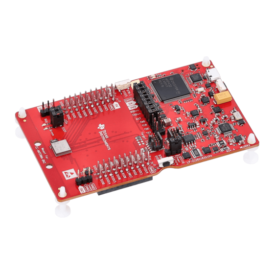
CC2651R3SIPA SimpleLink™ Multiprotocol 2.4 GHz Wireless System-in-Package
Module with integrated Antenna & 352-KB Memory
1 Features
Wireless microcontroller
•
Powerful 48-MHz Arm® Cortex®-M4 processor
•
352KB flash program memory
•
32KB of ultra-low leakage SRAM
•
8KB of Cache SRAM (Alternatively available as
general-purpose RAM)
•
Programmable radio includes support for 2-
(G)FSK, 4-(G)FSK, MSK, Bluetooth® 5.2 Low
Energy, IEEE 802.15.4 PHY and MAC
•
Supports over-the-air upgrade (OTA)
Low power consumption
•
MCU consumption:
– 3.60 mA active mode, CoreMark
– 61 μA/MHz running CoreMark
– 0.8 μA standby mode, RTC, 32KB RAM
– 0.1 μA shutdown mode, wake-up on pin
•
Radio Consumption:
– 6.8 mA RX
– 7.1 mA TX at 0 dBm
– 9.6 mA TX at +5 dBm
Wireless protocol support
•
Zigbee®
•
Bluetooth® 5.2 Low Energy
•
SimpleLink™ TI 15.4-stack
•
Proprietary systems
High performance radio
•
-104 dBm for Bluetooth® Low Energy 125-kbps
•
Output power up to +5 dBm with temperature
compensation
Regulatory compliance
•
Regulatory certification for compliance with
worldwide radio frequency:
– ETSI RED (Europe) / RER (UK)
– ISED (Canada)
– FCC (USA)
MCU peripherals
•
Digital peripherals can be routed to any GPIO
•
Four 32-bit or eight 16-bit general-purpose timers
•
12-bit ADC, 200 kSamples/s, 8 channels
•
8-bit DAC
•
Two comparators
•
Programmable current source
2
2
•
UART, SSI, I
C, I
S
An IMPORTANT NOTICE at the end of this data sheet addresses availability, warranty, changes, use in safety-critical applications,
intellectual property matters and other important disclaimers. PRODUCTION DATA.
SWRS278B – FEBRUARY 2022 – REVISED AUGUST 2023
•
Real-time clock (RTC)
•
Integrated temperature and battery monitor
Security enablers
•
AES 128-bit cryptographic accelerator
•
True random number generator (TRNG)
•
Additional cryptography drivers available in
Software Development Kit (SDK)
Development tools and software
•
LP-CC2651R3SIPA Development Kit
•
SimpleLink™ CC13xx and CC26xx Software
Development Kit (SDK)
•
SmartRF™ Studio
for simple radio configuration
•
SysConfig
system configuration tool
Operating range
•
On-chip buck DC/DC converter
•
1.8-V to 3.8-V single supply voltage
•
T
: -40 to +105°C
j
Package
•
7-mm × 7-mm MOU (32 GPIOs)
•
RoHS-compliant package
CC2651R3SIPA
Advertisement
Table of Contents

Related Manuals for Texas Instruments SimpleLink CC2651R3SIPA


Summary of Contents for Texas Instruments SimpleLink CC2651R3SIPA
-
Page 1: Features
CC2651R3SIPA SWRS278B – FEBRUARY 2022 – REVISED AUGUST 2023 CC2651R3SIPA SimpleLink™ Multiprotocol 2.4 GHz Wireless System-in-Package Module with integrated Antenna & 352-KB Memory • Real-time clock (RTC) 1 Features • Integrated temperature and battery monitor Wireless microcontroller Security enablers • Powerful 48-MHz Arm®... -
Page 2: Applications
For the most current part, package, and ordering information for all available devices, see the Package Option Addendum in Section 13, or see the website. RF Core for additional details on supported protocol standards, modulation formats, and data rates. Submit Document Feedback Copyright © 2023 Texas Instruments Incorporated Product Folder Links: CC2651R3SIPA... -
Page 3: Functional Block Diagram
SWRS278B – FEBRUARY 2022 – REVISED AUGUST 2023 4 Functional Block Diagram Figure 4-1 shows the functional block diagram of the CC2651R3SIPA module. Figure 4-1. CC2651R3SIPA Block Diagram Submit Document Feedback Copyright © 2023 Texas Instruments Incorporated Product Folder Links: CC2651R3SIPA... - Page 4 32 ch. µDMA Up to 32 GPIOs Time-to-Digital Converter Temperature and AES & TRNG Battery Monitor LDO, Clocks, and References Optional DC/DC Converter Figure 4-2. CC2651R3SIPA Hardware Overview Submit Document Feedback Copyright © 2023 Texas Instruments Incorporated Product Folder Links: CC2651R3SIPA...
-
Page 5: Table Of Contents
Added Korea, Japan, and Taiwan certifications....................46 • Added MIC (Japan) certification section......................• Added Korea certification section........................• Added NCC (Taiwan) certification section......................• Module layout guidelines updated........................Submit Document Feedback Copyright © 2023 Texas Instruments Incorporated Product Folder Links: CC2651R3SIPA... -
Page 6: Device Comparison
80 + 8 CC2652P7 144 + 8 ANTENNA RADIO SUPPORT CERTIFICATIONS PACKAGE SIZE Module CC2650MODA 20+8 CC2651R3SIPA 32 + 8 CC2652RSIP 80 + 8 CC2652PSIP 80 + 8 Submit Document Feedback Copyright © 2023 Texas Instruments Incorporated Product Folder Links: CC2651R3SIPA... -
Page 7: Terminal Configuration And Functions
Pin 2, DIO_27 • Pin 3, DIO_28 • Pin 7, DIO_29 • Pin 8, DIO_30 • Pin 35, DIO_23 • Pin 36, DIO_24 • Pin 39, DIO_25 Submit Document Feedback Copyright © 2023 Texas Instruments Incorporated Product Folder Links: CC2651R3SIPA... -
Page 8: Signal Descriptions - Sipa Package
DIO_9 Digital GPIO — — — — — — — — — — — — — — 51-59 — — INT_ANT RF connection to integral PCB antenna Submit Document Feedback Copyright © 2023 Texas Instruments Incorporated Product Folder Links: CC2651R3SIPA... -
Page 9: Connections For Unused Pins And Modules
PREFERRED FUNCTION SIGNAL NAME PIN NUMBER ACCEPTABLE PRACTICE PRACTICE 19-24 GPIO DIO_n NC or GND 27-36 41-50 X32K_Q2 32.768-kHz crystal X32K_Q1 No Connects NC = No connect Submit Document Feedback Copyright © 2023 Texas Instruments Incorporated Product Folder Links: CC2651R3SIPA... -
Page 10: Specifications
VDDS Brown-out Detector (BOD) Falling threshold 1.75 Brown-out Detector is trimmed at initial boot, value is kept until device is reset by a POR reset or the RESET_N pin Submit Document Feedback Copyright © 2023 Texas Instruments Incorporated Product Folder Links: CC2651R3SIPA... -
Page 11: Power Consumption - Power Modes
Delta current with clock enabled, module is idle 28.1 TRNG Delta current with clock enabled, module is idle 27.1 Only one UART running Only one SSI running Only one GPTimer running Submit Document Feedback Copyright © 2023 Texas Instruments Incorporated Product Folder Links: CC2651R3SIPA... -
Page 12: Power Consumption - Radio Modes
Semiconductor and IC Package Thermal Metrics. °C/W = degrees Celsius per watt. 8.9 RF Frequency Bands Over operating free-air temperature range (unless otherwise noted). PARAMETER UNIT Frequency bands 2360 2500 Submit Document Feedback Copyright © 2023 Texas Instruments Incorporated Product Folder Links: CC2651R3SIPA... -
Page 13: Antenna Characteristics
When measured on the LP-CC2651R3SIPA LaunchPad design with Tc = 25 °C. PARAMETER TEST CONDITIONS UNIT Polarization Linear Peak Gain 2.4 GHz Band Efficiency 2.4 GHz Band Submit Document Feedback Copyright © 2023 Texas Instruments Incorporated Product Folder Links: CC2651R3SIPA... -
Page 14: Bluetooth Low Energy - Receive (Rx)
Note that Image frequency + 1 MHz is the Co- channel Selectivity, Image frequency ±1 –1 MHz. Wanted signal at –72 dBm, modulated interferer 4 / 46 –3 at ±1 MHz from image frequency, BER = 10 Submit Document Feedback Copyright © 2023 Texas Instruments Incorporated Product Folder Links: CC2651R3SIPA... - Page 15 Selectivity, ±6 MHz 37 / 36 –3 MHz, BER = 10 Wanted signal at –67 dBm, modulated interferer at image Selectivity, image frequency –3 frequency, BER = 10 Submit Document Feedback Copyright © 2023 Texas Instruments Incorporated Product Folder Links: CC2651R3SIPA...
- Page 16 Numbers given as I/C dB X / Y, where X is +N MHz and Y is –N MHz Excluding one exception at F / 2, per Bluetooth Specification wanted Submit Document Feedback Copyright © 2023 Texas Instruments Incorporated Product Folder Links: CC2651R3SIPA...
-
Page 17: Bluetooth Low Energy - Transmit (Tx)
< 1 GHz, restricted bands FCC < –55 +5 dBm setting f > 1 GHz, including harmonics < –42 Second harmonic < –42 Harmonics Third harmonic < –42 Submit Document Feedback Copyright © 2023 Texas Instruments Incorporated Product Folder Links: CC2651R3SIPA... -
Page 18: (Oqpsk Dsss1:8, 250 Kbps) - Rx
Difference between incoming symbol rate and the internally Symbol rate error tolerance > 1000 generated symbol rate RSSI dynamic range RSSI accuracy ±4 Submit Document Feedback Copyright © 2023 Texas Instruments Incorporated Product Folder Links: CC2651R3SIPA... -
Page 19: (Oqpsk Dsss1:8, 250 Kbps) - Tx
The wakeup time is dependent on remaining charge on VDDR capacitor when starting the device, and thus how long the device has been in Reset or Shutdown before starting up again. Submit Document Feedback Copyright © 2023 Texas Instruments Incorporated Product Folder Links: CC2651R3SIPA... - Page 20 SWRS278B – FEBRUARY 2022 – REVISED AUGUST 2023 8.15.3 Clock Specifications 8.15.3.1 48 MHz Crystal Oscillator (XOSC_HF) Measured on a Texas Instruments reference design with integrated 48 MHz crystal including parameters based on external manufacturer's crystal specification at T = 25 °C, V = 3.0 V at initial time, unless otherwise noted.
- Page 21 Figure 8-1. SSI Timing for TI Frame Format (FRF = 01), Single Transfer Timing Measurement SSIClk SSIFss SSITx 8-bit control SSIRx 4 to 16 bits output data Figure 8-2. SSI Timing for MICROWIRE Frame Format (FRF = 10), Single Transfer Submit Document Feedback Copyright © 2023 Texas Instruments Incorporated Product Folder Links: CC2651R3SIPA...
- Page 22 Figure 8-3. SSI Timing for SPI Frame Format (FRF = 00), With SPH = 1 8.15.5 UART 8.15.5.1 UART Characteristics over operating free-air temperature range (unless otherwise noted) PARAMETER UNIT UART rate MBaud Submit Document Feedback Copyright © 2023 Texas Instruments Incorporated Product Folder Links: CC2651R3SIPA...
-
Page 23: Peripheral Characteristics
= 4.3 V × 1408 / 4095 Reference voltage VDDS as reference, input voltage scaling enabled VDDS VDDS / Reference voltage VDDS as reference, input voltage scaling disabled 2.82 Submit Document Feedback Copyright © 2023 Texas Instruments Incorporated Product Folder Links: CC2651R3SIPA... - Page 24 Applied voltage must be within Absolute Maximum Ratings (see Section 8.1) at all times No missing codes ADC_output = Σ(4 samples ) >> n, n = desired extra bits Submit Document Feedback Copyright © 2023 Texas Instruments Incorporated Product Folder Links: CC2651R3SIPA...
- Page 25 Max code output voltage = VDDS= 1.8 V ±2.10 variation Load = Continuous Time = DCOUPL, pre-charge ON ±6.00 Comparator = DCOUPL, pre-charge OFF ±3.85 = ADCREF ±5.84 Submit Document Feedback Copyright © 2023 Texas Instruments Incorporated Product Folder Links: CC2651R3SIPA...
- Page 26 = VDDS= 3.0 V ±0.55 = VDDS= 1.8 V ±0.60 Max code output voltage variation = DCOUPL, pre-charge ON ±3.45 = DCOUPL, pre-charge OFF ±2.10 = ADCREF ±1.90 Submit Document Feedback Copyright © 2023 Texas Instruments Incorporated Product Folder Links: CC2651R3SIPA...
- Page 27 3.8 V/3.0 V/1.8 V/DCOUPL/ADCREF) = 14.10 mV/11.13 mV/6.68 mV/4.67 mV/5.48 mV Includes comparator offset A load > 20 pF will increases the settling time Keysight 34401A Multimeter Submit Document Feedback Copyright © 2023 Texas Instruments Incorporated Product Folder Links: CC2651R3SIPA...
- Page 28 CC2651R3SIPA www.ti.com SWRS278B – FEBRUARY 2022 – REVISED AUGUST 2023 8.16.3 Temperature and Battery Monitor 8.16.3.1 Temperature Sensor Measured on a Texas Instruments reference design with T = 25 °C, V = 3.0 V, unless otherwise noted. PARAMETER TEST CONDITIONS...
- Page 29 = 25 °C, V = 3.0 V, unless otherwise noted. PARAMETER TEST CONDITIONS UNIT Current source programmable output range (logarithmic 0.25 - 20 µA range) Resolution 0.25 µA Submit Document Feedback Copyright © 2023 Texas Instruments Incorporated Product Folder Links: CC2651R3SIPA...
- Page 30 1 → 0 points = 25 °C Lowest GPIO input voltage reliably interpreted as a 0.8*V High Highest GPIO input voltage reliably interpreted as a 0.2*V Submit Document Feedback Copyright © 2023 Texas Instruments Incorporated Product Folder Links: CC2651R3SIPA...
-
Page 31: Typical Characteristics
Voltage [V] Temperature [ Figure 8-7. RX Current vs. Figure 8-6. RX Current vs. Supply Voltage (VDDS) (BLE 1 Mbps, 2.44 GHz) Temperature (BLE 1 Mbps, 2.44 GHz) Submit Document Feedback Copyright © 2023 Texas Instruments Incorporated Product Folder Links: CC2651R3SIPA... - Page 32 Figure 8-10. TX Current vs. Supply Voltage Figure 8-11. TX Current vs. Supply Voltage (VDDS) (BLE 1 Mbps, 2.44 GHz, 0 dBm) (VDDS) (BLE 1 Mpbs, 2.44 GHz, +5 dBm) Submit Document Feedback Copyright © 2023 Texas Instruments Incorporated Product Folder Links: CC2651R3SIPA...
- Page 33 TX Power Setting (SmartRF Studio) Typical Output Power [dBm] Typical Current Consumption [mA] 0xA42E 0x601E 0x246A 0x2E64 0x20A5 0x20A2 0x08DC -4.6 0x00D2 -9.0 0x00CD -12.7 0x00C8 -18.2 Submit Document Feedback Copyright © 2023 Texas Instruments Incorporated Product Folder Links: CC2651R3SIPA...
- Page 34 Voltage [V] Figure 8-16. Sensitivity vs. Figure 8-17. Sensitivity vs. Supply Voltage (VDDS) (BLE 1 Mbps, 2.44 GHz) Supply Voltage (VDDS) (BLE 1 Mbps, 2.44 GHz, DCDC Off) Submit Document Feedback Copyright © 2023 Texas Instruments Incorporated Product Folder Links: CC2651R3SIPA...
- Page 35 CC2651R3SIPA www.ti.com SWRS278B – FEBRUARY 2022 – REVISED AUGUST 2023 -100 -101 -102 -103 Voltage [V] Figure 8-18. Sensitivity vs. Supply Voltage (VDDS) (250 kbps, 2.44 GHz) Submit Document Feedback Copyright © 2023 Texas Instruments Incorporated Product Folder Links: CC2651R3SIPA...
- Page 36 Frequency [MHz] Figure 8-23. Output Power vs. Frequency Figure 8-24. Output Power vs. Frequency (BLE 1 Mbps, 2.44 GHz, 0 dBm) (BLE 1 Mbps, 2.44 GHz, +5 dBm) Submit Document Feedback Copyright © 2023 Texas Instruments Incorporated Product Folder Links: CC2651R3SIPA...
- Page 37 1.003 1.002 1.002 1.001 1.001 -40 -30 -20 -10 Voltage [V] Temperature [°C] Figure 8-30. ADC Accuracy vs. Figure 8-29. ADC Accuracy vs. Supply Voltage (VDDS) Temperature Submit Document Feedback Copyright © 2023 Texas Instruments Incorporated Product Folder Links: CC2651R3SIPA...
-
Page 38: Detailed Description
Tightly connected to 8-KB 4-way random replacement cache for minimal active power consumption and wait states • Ultra-low-power consumption with integrated sleep modes • 48 MHz operation • 1.25 DMIPS per MHz Submit Document Feedback Copyright © 2023 Texas Instruments Incorporated Product Folder Links: CC2651R3SIPA... -
Page 39: Radio (Rf Core)
Mchips per second Offset-QPSK with DSSS 1:8), used in the Zigbee protocol. The 802.15.4 PHY and MAC are in radio and system ROM. TI also provides royalty-free protocol stacks for Zigbee as part of the SimpleLink SDK, enabling a robust end-to-end solution. Submit Document Feedback Copyright © 2023 Texas Instruments Incorporated Product Folder Links: CC2651R3SIPA... -
Page 40: Memory
The cache can be used as a general-purpose RAM by enabling this feature in the Customer Configuration Area (CCFG). The ROM contains a serial (SPI and UART) bootloader that can be used for initial programming of the device. Submit Document Feedback Copyright © 2023 Texas Instruments Incorporated Product Folder Links: CC2651R3SIPA... - Page 41 Other capabilities, such as RSA encryption and signatures as well as Edwards type of elliptic curves such as Curve1174 or Ed25519, are a provided part of the TI SimpleLink SDK for the CC2651R3SIPA device. Submit Document Feedback Copyright © 2023 Texas Instruments Incorporated Product Folder Links: CC2651R3SIPA...
-
Page 42: Timers
The watchdog timer runs on a 1.5 MHz clock rate and cannot be stopped once enabled. The watchdog timer pauses to run in Standby power mode and when a debugger halts the device. Submit Document Feedback Copyright © 2023 Texas Instruments Incorporated Product Folder Links: CC2651R3SIPA... -
Page 43: Serial Peripherals And I/O
The on-chip debug support is done through a dedicated cJTAG (IEEE 1149.7) or JTAG (IEEE 1149.1) interface. The device boots by default into cJTAG mode and must be reconfigured to use 4-pin JTAG. Submit Document Feedback Copyright © 2023 Texas Instruments Incorporated Product Folder Links: CC2651R3SIPA... -
Page 44: Power Management
Therefore, TI highly recommends using this software framework for all application development on the device. The complete with TI-RTOS (optional), device drivers, and examples are offered free of charge in source code. Submit Document Feedback Copyright © 2023 Texas Instruments Incorporated Product Folder Links: CC2651R3SIPA... -
Page 45: Clock Systems
In the first case, the external host MCU communicates with the device using SPI or UART. In the second case, the application must be written according to the application framework supplied with the wireless protocol stack. Submit Document Feedback Copyright © 2023 Texas Instruments Incorporated Product Folder Links: CC2651R3SIPA... -
Page 46: Device Certification And Qualification
• This device may not cause harmful interference. • This device must accept any interference received, including interference that may cause undesired operation of the device. Submit Document Feedback Copyright © 2023 Texas Instruments Incorporated Product Folder Links: CC2651R3SIPA... -
Page 47: Added Mic (Japan) Certification Section
Radio Waves Act. In addition it is the responsibility of the OEM to ensure the Korea device, label, and user manual requirements are met per Table 9-3 Submit Document Feedback Copyright © 2023 Texas Instruments Incorporated Product Folder Links: CC2651R3SIPA... -
Page 48: Added Ncc (Taiwan) Certification Section
「平台商應於最終產品本體明顯處標示 本產品內含射頻模組 CCAF23Y10010T2 」。 • "The platform provider shall mark it clearly on the body of the final product: This product contains RF module CCAF23Y10010T2" Submit Document Feedback Copyright © 2023 Texas Instruments Incorporated Product Folder Links: CC2651R3SIPA... -
Page 49: Module Markings
The CC2651R3SIPAT0MOUR module is designed to comply with Korea statement, R-C-T3P-2651R3SIPA. The host system using this module must display a visible label indicating the following text in addition to the KC marking: • R-C-T3P-2651R3SIPA Submit Document Feedback Copyright © 2023 Texas Instruments Incorporated Product Folder Links: CC2651R3SIPA... -
Page 50: Manual Information To The End User
RF module in the user’s manual of the end product which integrates this module. The end user manual must include all required regulatory information and warnings as shown in this manual. Submit Document Feedback Copyright © 2023 Texas Instruments Incorporated Product Folder Links: CC2651R3SIPA... -
Page 51: Application, Implementation, And Layout
π or L matching and tuning may be required between RF out path, pin 14, and the external connection as shown in Figure 10-2. CC2651R3SIPA Figure 10-1. CC2651R3SIPA Typical Application Schematic Submit Document Feedback Copyright © 2023 Texas Instruments Incorporated Product Folder Links: CC2651R3SIPA... - Page 52 CC2651R3SIPA www.ti.com SWRS278B – FEBRUARY 2022 – REVISED AUGUST 2023 Figure 10-2. CC2651R3SIPA Typical Application Schematic for External Antenna Connection Submit Document Feedback Copyright © 2023 Texas Instruments Incorporated Product Folder Links: CC2651R3SIPA...
-
Page 53: Alternate Application Circuit
Section 10.1. For the full reference schematic, download the LP-CC2651R3SIPA Design Files. Submit Document Feedback Copyright © 2023 Texas Instruments Incorporated Product Folder Links: CC2651R3SIPA... - Page 54 CC2651R3SIPA www.ti.com SWRS278B – FEBRUARY 2022 – REVISED AUGUST 2023 Figure 10-3. CC2651R3SIPA Alternate Application Schematic Submit Document Feedback Copyright © 2023 Texas Instruments Incorporated Product Folder Links: CC2651R3SIPA...
-
Page 55: Device Connections
Have a solid ground plane and ground vias under the module for stable system and thermal dissipation. • Do not run signal traces underneath the module on a layer where the module is mounted. Submit Document Feedback Copyright © 2023 Texas Instruments Incorporated Product Folder Links: CC2651R3SIPA... -
Page 56: Module Layout Guidelines Updated
Overall 4-layer board thickness of 1.6 mm as per the reference design • The 4-layer dielectric constant of 4.0 +/- 0.2. Deviation from this will cause a potential detuning of the integrated antenna. Submit Document Feedback Copyright © 2023 Texas Instruments Incorporated Product Folder Links: CC2651R3SIPA... - Page 57 RF traces must be as short as possible. • The module must be as close to the PCB edge in consideration of the product enclosure and type of antenna being used. Submit Document Feedback Copyright © 2023 Texas Instruments Incorporated Product Folder Links: CC2651R3SIPA...
- Page 58 Table 10-5. Recommended Components CHOICE ANTENNA MANUFACTURER NOTES 2.4-GHz Inverted F Refer to 2.4-GHz Inverted F Antenna for details of the antenna Texas Instruments Antenna implementation and PCB requirements. Submit Document Feedback Copyright © 2023 Texas Instruments Incorporated Product Folder Links: CC2651R3SIPA...
- Page 59 GND and via stitching. Figure 10-6. Coplanar Waveguide (Cross Section) Figure 10-7. CPW With GND and Via Stitching (Top View) Submit Document Feedback Copyright © 2023 Texas Instruments Incorporated Product Folder Links: CC2651R3SIPA...
- Page 60 The ground loop should only be on the top layer of the board and not on all 4-layers. • A π matching network implementation in the ground loop allowing for tuning of the integrated antenna for optimal performance. Submit Document Feedback Copyright © 2023 Texas Instruments Incorporated Product Folder Links: CC2651R3SIPA...
-
Page 61: Reference Designs
Dual-band antennas for 868 MHz and 915 MHz combined with 2.4 GHz The antenna kit includes a JSC cable to connect to the Wireless MCU LaunchPad Development Kits and SensorTags. Submit Document Feedback Copyright © 2023 Texas Instruments Incorporated Product Folder Links: CC2651R3SIPA... -
Page 62: Junction Temperature Calculation
Typically, the easiest way to find the peak current consumption, and thus the peak power dissipation in the device, is to measure as described in Measuring CC13xx and CC26xx current consumption. Submit Document Feedback Copyright © 2023 Texas Instruments Incorporated Product Folder Links: CC2651R3SIPA... -
Page 63: Environmental Requirements And Smt
Monitor the solder paste volume (uniformity) • Package placement using standard SMT placement equipment • X-ray pre-reflow check - paste bridging • Reflow • X-ray post-reflow check - solder bridging and voids Submit Document Feedback Copyright © 2023 Texas Instruments Incorporated Product Folder Links: CC2651R3SIPA... -
Page 64: Baking Conditions
Humidity indicator cards read > 30% • Temp < 30°C, humidity < 70% RH, over 96 hours Baking condition: 90°C, 12 to 24 hours Baking times: 1 time Submit Document Feedback Copyright © 2023 Texas Instruments Incorporated Product Folder Links: CC2651R3SIPA... -
Page 65: Soldering And Reflow Condition
This coating can lead to localized stress on the solder connections inside the module and impact the module reliability. Use caution during the module assembly process to the final PCB to avoid the presence of foreign material inside the module. Submit Document Feedback Copyright © 2023 Texas Instruments Incorporated Product Folder Links: CC2651R3SIPA... -
Page 66: Device And Documentation Support
Predictions show that prototype devices (X or P) have a greater failure rate than the standard production devices. Texas Instruments recommends that these devices not be used in any production system because their expected end-use failure rate still is undefined. Only qualified production devices are to be used. - Page 67 For more information about the SimpleLink MCU Platform, visit http://www.ti.com/simplelink. Submit Document Feedback Copyright © 2023 Texas Instruments Incorporated Product Folder Links: CC2651R3SIPA...
- Page 68 SmartRF™ Studio is a Windows application that can be used to evaluate and configure SimpleLink Wireless MCUs from Texas Instruments. The application will help designers of RF systems to easily evaluate the radio at an early stage in the design process. It is especially useful for generation of configuration register values and for practical testing and debugging of the RF system.
-
Page 69: Documentation Support
® is a registered trademark of IAR Systems AB. ® Windows is a registered trademark of Microsoft Corporation. All trademarks are the property of their respective owners. Submit Document Feedback Copyright © 2023 Texas Instruments Incorporated Product Folder Links: CC2651R3SIPA... -
Page 70: Electrostatic Discharge Caution
SWRS278B – FEBRUARY 2022 – REVISED AUGUST 2023 12.6 Electrostatic Discharge Caution This integrated circuit can be damaged by ESD. Texas Instruments recommends that all integrated circuits be handled with appropriate precautions. Failure to observe proper handling and installation procedures can cause damage. -
Page 71: Information
For browser-based versions of this data sheet, refer to the left-hand navigation. Note The total height of the module is 1.51 mm. The weight of the CC2651R3SIPA module is typically 0.182 g. Submit Document Feedback Copyright © 2023 Texas Instruments Incorporated Product Folder Links: CC2651R3SIPA... - Page 72 PACKAGE OPTION ADDENDUM www.ti.com 21-Sep-2022 PACKAGING INFORMATION Orderable Device Status Package Type Package Pins Package Eco Plan Lead finish/ MSL Peak Temp Op Temp (°C) Device Marking Samples Drawing Ball material (4/5) CC2651R3SIPAT0MOUR ACTIVE 2000 RoHS (In ENEPIG Level-3-260C-168 HR -40 to 105 CC2651 Samples...
- Page 73 PACKAGE MATERIALS INFORMATION www.ti.com 21-Sep-2022 TAPE AND REEL INFORMATION REEL DIMENSIONS TAPE DIMENSIONS B0 W Reel Diameter Cavity Dimension designed to accommodate the component width Dimension designed to accommodate the component length Dimension designed to accommodate the component thickness Overall width of the carrier tape Pitch between successive cavity centers Reel Width (W1) QUADRANT ASSIGNMENTS FOR PIN 1 ORIENTATION IN TAPE...
- Page 74 PACKAGE MATERIALS INFORMATION www.ti.com 21-Sep-2022 TAPE AND REEL BOX DIMENSIONS Width (mm) *All dimensions are nominal Device Package Type Package Drawing Pins Length (mm) Width (mm) Height (mm) CC2651R3SIPAT0MOUR 2000 336.6 336.6 31.8 Pack Materials-Page 2...
- Page 75 PACKAGE OUTLINE MOU0050A QFM - 1.51 mm max height SCALE 2.200 QUAD FLAT MODULE PIN 1 CORNER 1.51 1.35 SEATING PLANE 0.372 0.1 C 0.292 0.338 46 X 0.262 0.538 46 X 0.462 0.15 C A B 0.05 0.338 0.262 0.15 C A B 0.05...
- Page 76 0.05 MIN ALL AROUND LAND PATTERN EXAMPLE SOLDER MASK DEFINED SCALE:15X 4226342/B 12/2020 NOTES: (continued) 3. This package is designed to be soldered to a thermal pad on the board. For more information, see Texas Instruments literature number SLUA271 (www.ti.com/lit/slua271). www.ti.com...
- Page 77 EXAMPLE STENCIL DESIGN MOU0050A QFM - 1.51 mm max height QUAD FLAT MODULE (6.2) 4 X ( 0.5) 7 X (0.6) 46 X (0.5) (0.5) (6.2) (R0.05) 9 X ( 0.3) (1.6) 46 X (0.3) SOLDER PASTE EXAMPLE BASED ON 0.125 mm THICK STENCIL SCALE:15X 4226342/B 12/2020 NOTES: (continued)
- Page 78 TI products. TI’s provision of these resources does not expand or otherwise alter TI’s applicable warranties or warranty disclaimers for TI products. TI objects to and rejects any additional or different terms you may have proposed. IMPORTANT NOTICE Mailing Address: Texas Instruments, Post Office Box 655303, Dallas, Texas 75265 Copyright © 2023, Texas Instruments Incorporated...
Need help?
Do you have a question about the SimpleLink CC2651R3SIPA and is the answer not in the manual?
Questions and answers