Table of Contents
Advertisement
Quick Links
FEATURES
Single-supply voltage: 3.3 V
►
Wide frequency range: DC to 18 GHz
►
SMA connectors for RF signals
►
Parallel interface and SPI
►
On-board calibration thru transmission line for analyzer calibra-
►
tion
EVALUATION KIT CONTENTS
EVAL-ADGM1144SDZ evaluation board
►
ADDITIONAL EQUIPMENT NEEDED
3.3 V DC power supply
►
Vector network analyzer (VNA)
►
EVAL-SDP-CB1Z (SDP-B)
►
Analysis | Control | Evaluation (ACE) Software
►
ADGM1144SDZ plugin
GENERAL DESCRIPTION
This user guide describes the EVAL-ADGM1144SDZ for the
ADGM1144, a dual-chip, RF switching solution containing a single-
pole, four-throw (SP4T), microelectromechanical systems (MEMS)
switch, and a control chip copackaged in a compact, 5.00 mm ×
4.00 mm × 1.0 mm, LGA package.
The SP4T switch uses Analog Devices, Inc., MEMS switch tech-
nology, providing optimum performance in terms of bandwidth,
power handling capability, and linearity for RF applications. The
control chip generates the high-voltage signals needed for the
MEMS switch and allows the user to control its operation through
a simple and flexible complementary metal-oxide semiconductor
(CMOS)/low voltage transistor to transistor logic (LVTTL)-compliant
parallel-interface as well as through a serial-peripheral interface
(SPI). It is possible to daisy-chain multiple ADGM1144 devices
together to enable the configuration of multiple devices with a
minimal number of digital lines.
For SPI, the EVAL-ADGM1144SDZ connects to the USB port of
a PC via the SDP board. The EVAL-SDP-CB1Z board (SDP-B con-
troller board) is available to order at the Analog Devices website.
The EVAL-ADGM1144SDZ comes fitted with connectors for RF and
control signals as well as links to control the operation of the switch
and evaluate its performance.
For full details on the ADGM1144, see the ADGM1144 data sheet,
which must be consulted in conjunction with this user guide when
using the EVAL-ADGM1144SDZ.
PLEASE SEE THE LAST PAGE FOR AN IMPORTANT
WARNING AND LEGAL TERMS AND CONDITIONS.
Evaluating the ADGM1144 0 Hz/DC to 18 GHz, SP4T, MEMS Switch
controller board
with EVAL-
User Guide | EVAL-ADGM1144
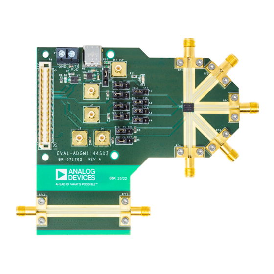
EVAL-ADGM1144SDZ PHOTOGRAPH
UG-2056
Figure 1.
Rev. 0 | 1 of 18
Advertisement
Table of Contents

Related Manuals for Analog Devices EVAL-ADGM1144SDZ


Summary of Contents for Analog Devices EVAL-ADGM1144SDZ
-
Page 1: Features
For SPI, the EVAL-ADGM1144SDZ connects to the USB port of a PC via the SDP board. The EVAL-SDP-CB1Z board (SDP-B con- troller board) is available to order at the Analog Devices website. -
Page 2: Table Of Contents
User Guide EVAL-ADGM1144 TABLE OF CONTENTS Features..............1 EVAL-ADGM1144SDZ Block Diagram and Evaluation Kit Contents......... 1 Descriptions............6 Additional Equipment Needed....... 1 Memory Map............7 General Description..........1 Measuring Switch Performance......8 EVAL-ADGM1144SDZ Photograph....... 1 Network Analyzer Calibration Procedure.....10 Evaluation Board Hardware........3 Handling Guidelines..........11 Power Supply............. -
Page 3: Evaluation Board Hardware
K1 to K4 links. When the P5 link is set to the PIN position, the the EVAL-ADGM1144SDZ is powered by the Mini-USB connector, SPI is enabled. When the P5 link is set to the SPI position, the and when JP7 is in the B position, the EVAL-ADGM1144SDZ is parallel-interface is enabled (see Table powered by the external 3.3 V power supply through the power... - Page 4 User Guide EVAL-ADGM1144 EVALUATION BOARD HARDWARE Table 5. Link Settings (Per PCB Label) for Parallel-Interface Use (See Figure Controlled RF Switch RF Switch Status Link Name Link Position RF3 to RFC Off (default) IN-3 (default) IN-3 RF4 to RFC Off (default) IN-4 (default) IN-4 analog.com...
-
Page 5: Evaluation Board Software For The Spi
3. Change the P5 link position from PIN to SPI and keep the P6 link position at INT. 4. Connect the EVAL-ADGM1144SDZ to the SDP board and con- nect the SDP board to the computer via a USB cable. 5. Power the EVAL-ADGM1144SDZ as described in the Power Figure 4. -
Page 6: Eval-Adgm1144Sdz Block Diagram And Descriptions
User Guide EVAL-ADGM1144 EVAL-ADGM1144SDZ BLOCK DIAGRAM AND DESCRIPTIONS The EVAL-ADGM1144SDZ software is organized so that it appears similar to the functional block diagram shown in the ADGM1144 data sheet.. A full description of each block and register, as well as their respective settings, are given in the ADGM1144 data sheet. -
Page 7: Memory Map
Any bits or registers that are bold in Figure 6 are modified values that have not been transferred to the EVAL-ADGM1144SDZ. Click Apply Changes to transfer data to the EVAL-ADGM1144SDZ. Figure 6. ADGM1144 Memory Map analog.com... -
Page 8: Measuring Switch Performance
Network Analyzer Calibration Procedure section for more information. Figure 8. EVAL-ADGM1144SDZ Calibration Transmission Line Used for PCB Insertion Loss and Phase Offset Correction Use the network analyzer port extension function to de-embed any phase offset introduced by the PCB transmission lines. The port extension method uses time delay offset values to correct for phase. - Page 9 User Guide EVAL-ADGM1144 MEASURING SWITCH PERFORMANCE Figure 11 shows the ADGM1144 switch insertion loss measurement results of all four channels that are de-embedded with respect to the PCB transmission line losses. Figure 13. ADGM1144 Off-Isolation Performance Figure 11. PCB De-Embedded ADGM1144 Insertion Loss Performance Figure 12 shows the ADGM1144 switch return loss performance measurement results for all four channels.
-
Page 10: Network Analyzer Calibration Procedure
The maximum value for the network analyzer fre- measurement using the data saved at Step 3 and the measured quency sweep for the EVAL-ADGM1144SDZ PCB can be up to 20 data at Step 6. Because the extraction method is dependent on GHz. -
Page 11: Handling Guidelines
User Guide EVAL-ADGM1144 HANDLING GUIDELINES Adhere to the following handling guidelines for the EVAL- ADGM1144SDZ: Always treat the ADGM1144 as a static sensitive device and ► observe normal handling precautions, including working only on static dissipative surfaces, wearing wrist straps, or other electro- static discharge (ESD) control devices. -
Page 12: Layout Recommendations
User Guide EVAL-ADGM1144 LAYOUT RECOMMENDATIONS The EVAL-ADGM1144SDZ is a 4-layer board. The EVAL- ADGM1144SDZ uses 8 mil Roger RO4003C dielectric. The outer copper layers have 2.2 mil finish thickness with electroless nickel immersion gold (ENIG) finish. The RF transmission lines were... -
Page 13: Soldering Recommendations
User Guide EVAL-ADGM1144 SOLDERING RECOMMENDATIONS To avoid solder voids under the ADGM1144, it is recommended to use a 0.0767 mm (3 mil) thick solder stencil with nano coating. The aperture size for the solder stencil must be 1:1, and divide the paste mask with multiple pads, as shown in Figure 16. -
Page 14: Evaluation Board Schematics And Artwork
User Guide EVAL-ADGM1144 EVALUATION BOARD SCHEMATICS AND ARTWORK Figure 17. Schematic of the EVAL-ADGM1144SDZ analog.com Rev. 0 | 14 of 18... - Page 15 User Guide EVAL-ADGM1144 EVALUATION BOARD SCHEMATICS AND ARTWORK Figure 18. Schematic of the EVAL-ADGM1144SDZ with an SDP Connector Figure 19. EVAL-ADGM1144SDZ Component Side PCB Drawing (Layer 1) analog.com Rev. 0 | 15 of 18...
- Page 16 User Guide EVAL-ADGM1144 EVALUATION BOARD SCHEMATICS AND ARTWORK Figure 20. EVAL- ADGM1144SDZ Component Side Ground Plane PCB Drawing (Layer 2) Figure 21. EVAL- ADGM1144SDZ Component Side Ground Plane PCB Drawing (Layer 3) Figure 22. EVAL- ADGM1144SDZ Component Side, Bottom Side PCB Drawing (Layer 4) analog.com Rev.
- Page 17 User Guide EVAL-ADGM1144 EVALUATION BOARD SCHEMATICS AND ARTWORK Figure 23. EVAL-ADGM1144SDZ Component Side Silkscreen PCB Drawing (Top) Figure 24. EVAL-ADGM1144SDZ Soldermask Top Figure 25. EVAL-ADGM1144SDZ Paste Top analog.com Rev. 0 | 17 of 18...
-
Page 18: Ordering Information
Evaluation Board until you have read and agreed to the Agreement. Your use of the Evaluation Board shall signify your acceptance of the Agreement. This Agreement is made by and between you (“Customer”) and Analog Devices, Inc. (“ADI”), with its principal place of business at Subject to the terms and conditions of the Agreement, ADI hereby grants to Customer a free, limited, personal, temporary, non-exclusive, non-sublicensable, non-transferable license to use the Evaluation Board FOR EVALUATION PURPOSES ONLY.
Need help?
Do you have a question about the EVAL-ADGM1144SDZ and is the answer not in the manual?
Questions and answers