Table of Contents
Advertisement
Quick Links
One Technology Way • P.O. Box 9106 • Norwood, MA 02062-9106, U.S.A. • Tel: 781.329.4700 • Fax: 781.461.3113 • www.analog.com
Evaluating the
ADGS1208/ADGS1209
FEATURES
SPI interface with error detection
Includes CRC error detection, invalid read/write address
detection, and SCLK count error detection
Analog supply voltages
Dual supply: ±15 V
Single supply: 12 V
PC control in conjunction with evaluation software
EVALUATION KIT CONTENTS
EVAL-ADGS1208SDZ/EVAL-ADGS1209SDZ
EQUIPMENT NEEDED
EVAL-SDP-CB1Z
controller board
ACE software
with EVAL-ADGS1208SDZ/
EVAL-ADGS1209SDZ plugin
DC voltage source
±15 V for dual-supply
12 V for single-supply
Optional digital logic supply: 3.3 V
Analog signal source
Digital multimeter
DOCUMENTS NEEDED
ADGS1208/ADG1209
data sheet
PLEASE SEE THE LAST PAGE FOR AN IMPORTANT
WARNING AND LEGAL TERMS AND CONDITIONS.
EVAL-ADGS1208SDZ/EVAL-ADGS1209SDZ
1.8 V Logic Control, 8:1/Dual 4:1 Mux Switches
SPI Interface, Low C
GENERAL DESCRIPTION
The EVAL-ADGS1208SDZ/EVAL-ADGS1209SDZ are the
evaluation boards for the ADGS1208/ADGS1209. The
ADGS1208/ADGS1209
charge injection (Q
serial peripheral interface (SPI). The SPI has robust error detection
features, including cyclic redundancy check (CRC) error
detection, invalid read/write address detection, and serial clock
(SCLK) count error detection. It is possible to daisy-chain multiple
ADGS1208/ADGS1209
configuration of multiple devices with a minimal amount of digital
lines. The
ADGS1208/ADGS1209
decreases the time between SPI commands.
Figure 1 shows the EVAL-ADGS1208SDZ/EVAL-ADGS1209SDZ
typical evaluation board setup. The EVAL-ADGS1208SDZ/
EVAL-ADGS1209SDZ are controlled by the
system demonstration platform (SDP), which connects to a PC
via a USB port. The
the evaluation board, and wire screw terminals are provided to
connect to each source and drain pin. Three screw terminals
power the device and, if required, a fourth terminal provides
users with a defined digital logic supply voltage. Alternatively,
the digital logic supply voltage can be supplied from the SDP.
Consult the
ADGS1208/ADGS1209
Analog Devices, Inc.) in conjunction with this user guide.
The evaluation board interfaces to the USB port of a PC via the
SDP board. The
board) is available for order at www.analog.com/SDP-B.
Rev. 0 | Page 1 of 17
and Q
, ±15 V/+12 V,
ON
INJ
are low on capacitance (C
), 8:1/dual 4:1 multiplexers controlled by a
INJ
devices together to enable the
also support burst mode, which
EVAL-SDP-CB1Z
ADGS1208
or
ADGS1209
data sheet (available from
EVAL-SDP-CB1Z
board (SDP-B controller
User Guide
UG-1271
), low
ON
is on the center of
Advertisement
Table of Contents

Related Manuals for Analog Devices EVAL-ADGS1208SDZ


Summary of Contents for Analog Devices EVAL-ADGS1208SDZ
-
Page 1: Features
ADGS1208/ADG1209 data sheet Consult the ADGS1208/ADGS1209 data sheet (available from Analog Devices, Inc.) in conjunction with this user guide. The evaluation board interfaces to the USB port of a PC via the SDP board. The EVAL-SDP-CB1Z board (SDP-B controller board) is available for order at www.analog.com/SDP-B. -
Page 2: Table Of Contents
Revision History ................2 Memory Map .................6 Evaluation Board Photographs ............3 Evaluation Board Schematics and Artwork ........8 Evaluation Board Hardware ............4 EVAL-ADGS1208SDZ ..............8 Power Supplies ................4 EVAL-ADGS1209SDZ ............... 13 Input Signals .................. 4 Ordering Information ..............17 Digital Outputs ................ -
Page 3: Evaluation Board Photographs
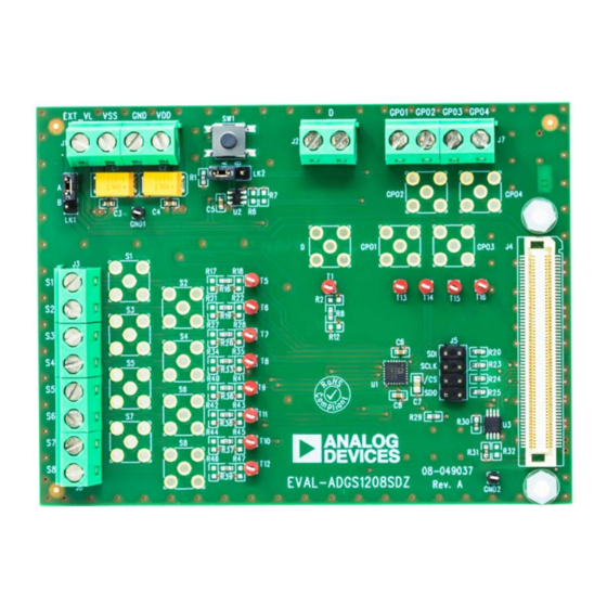
EVAL-ADGS1208SDZ/EVAL-ADGS1209SDZ User Guide UG-1271 EVALUATION BOARD PHOTOGRAPHS Figure 1. EVAL-ADGS1208SDZ Figure 2. EVAL-ADGS1209SDZ Rev. 0 | Page 3 of 17... -
Page 4: Evaluation Board Hardware
J1. LK1 must be in Position A. LK1 must be in Position B to avoid damaging the SDP when INPUT SIGNALS using it in conjunction with the EVAL-ADGS1208SDZ/ Provided are screw connectors J2, J3, and J6 to connect to both EVAL-ADGS1209SDZ. -
Page 5: Evaluation Board Software Quick Start Procedures
SDP board and connect the SDP board to the PC via a USB cable. Turn on the evaluation board as described in the Power Figure 3. Evaluation Board View of the EVAL-ADGS1208SDZ/ Supplies section. EVAL-ADGS1209SDZ Rev. 0 | Page 5 of 17... -
Page 6: Block Diagram And Description
The SW Reset button causes the device to perform a software reset. The GPO1, GPO2, GPO3, and GPO4 buttons select whether the corresponding GPO is on or off. Figure 4. EVAL-ADGS1208SDZ/EVAL-ADGS1209SDZ Block Diagram with Labels Rev. 0 | Page 6 of 17... - Page 7 EVAL-ADGS1208SDZ/EVAL-ADGS1209SDZ User Guide UG-1271 Figure 5. ADGS1208/ADGS1209 Memory Map Figure 6. ADGS1208/ADGS1209 Memory Map with Unapplied Changes in the SW_DATA Register Rev. 0 | Page 7 of 17...
-
Page 8: Evaluation Board Schematics And Artwork
UG-1271 EVAL-ADGS1208SDZ/EVAL-ADGS1209SDZ User Guide EVALUATION BOARD SCHEMATICS AND ARTWORK EVAL-ADGS1208SDZ Figure 7. EVAL-ADGS1208SDZ Schematic 1 Rev. 0 | Page 8 of 17... - Page 9 EVAL-ADGS1208SDZ/EVAL-ADGS1209SDZ User Guide UG-1271 Figure 8. EVAL-ADGS1208SDZ Schematic 2 Rev. 0 | Page 9 of 17...
- Page 10 UG-1271 EVAL-ADGS1208SDZ/EVAL-ADGS1209SDZ User Guide Figure 9. EVAL-ADGS1208SDZ Schematic 3 Figure 10. EVAL-ADGS1208SDZ Schematic 4 Rev. 0 | Page 10 of 17...
- Page 11 EVAL-ADGS1208SDZ/EVAL-ADGS1209SDZ User Guide UG-1271 Figure 11. EVAL-ADGS1208SDZ Silk Screen Figure 12. EVAL-ADGS1208SDZ Top Layer Figure 13. EVAL-ADGS1208SDZ Layer 2 Rev. 0 | Page 11 of 17...
- Page 12 UG-1271 EVAL-ADGS1208SDZ/EVAL-ADGS1209SDZ User Guide Figure 14. EVAL-ADGS1208SDZ Layer 3 Figure 15. EVAL-ADGS1208SDZ Bottom Layer Rev. 0 | Page 12 of 17...
-
Page 13: Eval-Adgs1209Sdz
EVAL-ADGS1208SDZ/EVAL-ADGS1209SDZ User Guide UG-1271 EVAL-ADGS1209SDZ Figure 16. EVAL-ADGS1209SDZ Schematic 1 Figure 17. EVAL-ADGS1209SDZ Schematic 2 Rev. 0 | Page 13 of 17... - Page 14 UG-1271 EVAL-ADGS1208SDZ/EVAL-ADGS1209SDZ User Guide Figure 18. EVAL-ADGS1209SDZ Schematic 3 Figure 19. EVAL-ADGS1209SDZ Schematic 4 Rev. 0 | Page 14 of 17...
- Page 15 EVAL-ADGS1208SDZ/EVAL-ADGS1209SDZ User Guide UG-1271 Figure 20. EVAL-ADGS1209SDZ Silk Screen Figure 21. EVAL-ADGS1209SDZ Top Layer Figure 22. EVAL-ADGS1209SDZ Layer 2 Rev. 0 | Page 15 of 17...
- Page 16 UG-1271 EVAL-ADGS1208SDZ/EVAL-ADGS1209SDZ User Guide Figure 23. EVAL-ADGS1209SDZ Layer 3 Figure 24. EVAL-ADGS1209SDZ Bottom Layer Rev. 0 | Page 16 of 17...
-
Page 17: Ordering Information
By using the evaluation board discussed herein (together with any tools, components documentation or support materials, the “Evaluation Board”), you are agreeing to be bound by the terms and conditions set forth below (“Agreement”) unless you have purchased the Evaluation Board, in which case the Analog Devices Standard Terms and Conditions of Sale shall govern. Do not use the Evaluation Board until you have read and agreed to the Agreement.
Need help?
Do you have a question about the EVAL-ADGS1208SDZ and is the answer not in the manual?
Questions and answers