Table of Contents
Advertisement
Quick Links
One Technology Way • P.O. Box 9106 • Norwood, MA 02062-9106, U.S.A. • Tel: 781.329.4700 • Fax: 781.461.3113 • www.analog.com
Evaluating the
ADGM1004
FEATURES
Single supply voltage 3.3 V
Wide frequency range
SMA connectors for RF signals
SMB connectors for switch control signals
On-board calibration transmission line for analyzer calibration
EVALUATION KIT CONTENTS
EVAL-ADGM1004SDZ evaluation board
DOCUMENTS NEEDED
ADGM1004
data sheet
EQUIPMENT NEEDED
3.3 V dc power supply
PC
EVAL-SDP-CB1Z
controller board
USB cable, provided in
EVAL-SDP-CB1Z
Vector network analyzer
GENERAL DESCRIPTION
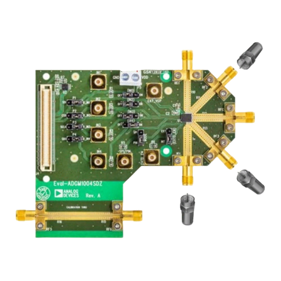
The EVAL-ADGM1004SDZ evaluates the
wideband, single-pole, four-throw (SP4T), microelectromechanical
systems (MEMS) switch, and a control chip copackaged in a
compact, 24-lead, 5 mm × 4 mm × 1.45 mm, lead frame chip scale
package (LFCSP). The SP4T switch uses Analog Devices, Inc.,
PLEASE SEE THE LAST PAGE FOR AN IMPORTANT
WARNING AND LEGAL TERMS AND CONDITIONS.
0 Hz/DC to 13 GHz, 2.5 kV HBM ESD, SP4T MEMS Switch
with Integrated Driver
board kit
ADGM1004
Rev. 0 | Page 1 of 18
EVAL-ADGM1004SDZ
MEMS switch technology, which provides optimum bandwidth
performance, power handling capability, and linearity for radio
frequency applications. The control chip generates the high voltage
signals necessary for the MEMS switch and allows the user to
control operation through a flexible, complementary metal oxide
semiconductor (CMOS), low voltage transistor to transistor logic
(LVTTL) compliant, parallel interface, as well as through a
serial peripheral interface (SPI). It is possible to daisy-chain
multiple
ADGM1004
devices together, which enables the
configuration of multiple devices with a minimal amount of
digital lines.
For the SPI interface, the EVAL-ADGM1004SDZ connects to
the USB port of a PC via a system demonstration platform
(SDP) board. The
EVAL-SDP-CB1Z
acceptable to use, and is available to order on the Analog
Devices website at www.analog.com/SDP-B.
The EVAL-ADGM1004SDZ is fitted with connectors for RF and
control signals, as well as links that allow the user to control the
operation of the switch and evaluate the performance of the
ADGM1004.
For full specifications on the ADGM1004, consult the
ADGM1004
data sheet, which must be used in conjunction with
this user guide when using the EVAL-ADGM1004SDZ.
User Guide
UG-1462
(SDP-B) controller board is
Advertisement
Table of Contents

Related Manuals for Analog Devices EVAL-ADGM1004SDZ


Summary of Contents for Analog Devices EVAL-ADGM1004SDZ
-
Page 1: Features
USB cable, provided in EVAL-SDP-CB1Z board kit The EVAL-ADGM1004SDZ is fitted with connectors for RF and Vector network analyzer control signals, as well as links that allow the user to control the operation of the switch and evaluate the performance of the GENERAL DESCRIPTION ADGM1004. -
Page 2: Table Of Contents
UG-1462 EVAL-ADGM1004SDZ User Guide TABLE OF CONTENTS Features ....................1 Installing the Software ..............6 Evaluation Kit Contents ..............1 Initial Setup ..................6 Documents Needed ................1 Block Diagram and Description ............7 Equipment Needed ................1 Memory Map .................8... -
Page 3: Evaluation Board Connection Diagram
EVAL-ADGM1004SDZ User Guide UG-1462 EVALUATION BOARD CONNECTION DIAGRAM Figure 1 shows the evaluation board connect diagram. NETWORK ANALYZER POWER SUPPLY 3.3V dc – – 50Ω 50Ω 50Ω Figure 1. Rev. 0 | Page 3 of 18... -
Page 4: Evaluation Board Hardware
(PCB). The internal control IC co-packaged with the MEMS switch The EVAL-ADGM1004SDZ allows the RF signals to connect to generates the voltage required to drive the switch. The control the MEMS switch. Control the switch operation either by using IC generates a reference clock signal at 10 MHz. - Page 5 EVAL-ADGM1004SDZ User Guide UG-1462 Table 4. P1 to P4 and IN1 to IN4 Link Settings for Parallel Logic Interface Controlled RF Switch RF Switch Status Link Name Link Position RF1 to RFC D_IN1 D_IN1 (default) Off (default) RF2 to RFC...
-
Page 6: Evaluation Board Software For Spi Interface
SDP-B board to the EVAL-ADGM1004SDZ. Find the software and access to full instructions on how to install and use the software on the Analog Devices website at www.analog.com/ace. When the installation is finished, the software starts and the EVAL-ADGM1004SDZ plugins appear. -
Page 7: Block Diagram And Description
Some blocks and the corresponding functions pertain to the RFC switch. EVAL-ADGM1004SDZ, and are described in Table 6. The full Click the switch symbol to open and close the RF4 to screen block diagram shown in Figure 5 displays the RFC switch. -
Page 8: Memory Map
UG-1462 EVAL-ADGM1004SDZ User Guide MEMORY MAP software. All other bits are toggled. The Apply Changes button transfers data to the device. All changes made in this tab All registers are fully accessible from the ADGM1004 Memory correspond to the block diagram. -
Page 9: Measuring Switch Performance
A and B. Both A and B are identical in length, and can be calculated by measuring the time delay of the calibration transmission line and dividing it by 2. Figure 7. EVAL-ADGM1004SDZ Calibration Transmission Line for PCB Insertion Loss and Phase Offset Correction –0.5 –10... - Page 10 UG-1462 EVAL-ADGM1004SDZ User Guide Figure 10 shows the ADGM1004 switch insertion loss (network Figure 11 shows the ADGM1004 switch off isolation performance analyzer two-port S(2,1) measurement) measurement results that measurement results for two channels. The blue trace is the RF2...
-
Page 11: Network Analyzer Calibration Procedure
The maximum value of the network analyzer frequency sweep for De-embed the PCB losses from the complete EVAL- the EVAL-ADGM1004SDZ PCB can be up to 16 GHz. Assuming ADGM1004SDZ measurement using the data saved from the user has a set of manual calibration standards or an electric Step 3 and the measured data from Step 6. -
Page 12: Handling Guidelines
(ESD) Physically handle the EVAL-ADGM1004SDZ with care. control devices. Take care when connecting signals. Hold the EVAL- ADGM1004SDZ from the edges to avoid any damage to the device under test (DUT). -
Page 13: Evaluation Board Schematics And Artwork
EVAL-ADGM1004SDZ User Guide UG-1462 EVALUATION BOARD SCHEMATICS AND ARTWORK Figure 12. EVAL-ADGM1004SDZ Schematic Rev. 0 | Page 13 of 18... - Page 14 UG-1462 EVAL-ADGM1004SDZ User Guide Figure 13. EVAL-ADGM1004SDZ Schematic with SDP-B Board Rev. 0 | Page 14 of 18...
- Page 15 EVAL-ADGM1004SDZ User Guide UG-1462 Figure 14. EVAL-ADGM1004SDZ Component Side, PCB Drawing (Layer 1) Figure 15. EVAL-ADGM1004SDZ Component Side, Ground Plane PCB Drawing (Layer 2) Rev. 0 | Page 15 of 18...
- Page 16 UG-1462 EVAL-ADGM1004SDZ User Guide Figure 16. EVAL-ADGM1004SDZ Component Side, Ground Plane PCB Drawing (Layer 3) Figure 17. EVAL-ADGM1004SDZ Component Side, Bottom Side PCB Drawing (Layer 4) Rev. 0 | Page 16 of 18...
- Page 17 CPWG RF TRACE TO GROUND GAP:12.2 THOU FINAL OVERALL PCB THICKNESS:62 THOU FINAL COPPER PLATING THICKNESS ON TOP AND BOTTOM LAYERS: 1.5oz Figure 19. EVAL-ADGM1004SDZ PCB Stackup with Coplanar Waveguide and Ground (CPWG) Dimensions Rev. 0 | Page 17 of 18...
-
Page 18: Ordering Information
By using the evaluation board discussed herein (together with any tools, components documentation or support materials, the “Evaluation Board”), you are agreeing to be bound by the terms and conditions set forth below (“Agreement”) unless you have purchased the Evaluation Board, in which case the Analog Devices Standard Terms and Conditions of Sale shall govern. Do not use the Evaluation Board until you have read and agreed to the Agreement.
Need help?
Do you have a question about the EVAL-ADGM1004SDZ and is the answer not in the manual?
Questions and answers