
Subscribe to Our Youtube Channel
Related Manuals for Broadcom BCM91250A


Summary of Contents for Broadcom BCM91250A
- Page 1 USER MANUAL BCM91250A Evaluation Board 91250A-UM100-R 16215 Alton Parkway • P.O. Box 57013 • Irvine, CA 92619-7013 • Phone: 949-450-8700 • Fax: 949-450-8710 05/18/04...
- Page 2 All rights reserved Printed in the U.S.A. ® Broadcom and the pulse logo are registered trademarks of Broadcom Corporation and/or its subsidiaries in the United States and certain other countries. All other trademarks mentioned are the property of their respective owners.
-
Page 3: Table Of Contents
Items Included with Your Shipment ......................1 Features ................................ 1 Hardware ..............................1 Firmware ..............................2 BCM91250A Front Panel..........................3 BCM91250A Rear Panel ..........................3 Section 2: Getting Started....................4 Section 3: Physical Description ..................6 Block Diagram .............................. 7 Connectors ..............................8 Board Connectors ........................... - Page 4 BCM91250A User Manual 05/18/04 Section 6: Web Resources ....................26 SiByte................................26 Peripherals ..............................26 Bus Interface ...............................27 Bro adco m C orp or atio n Page Document 91250A-UM100-R...
- Page 5 User Manual BCM91250A 05/18/04 IST OF IGURES Figure 1: BCM91250A Front Panel........................ 3 Figure 2: BCM91250A Rear Panel ........................ 3 Figure 3: BCM91250A Top View ........................6 Figure 4: BCM91250A Block Diagram......................7 Figure 5: Connector Callouts ......................... 8 Figure 6: IDE Connector (J35) Pin 20 Rework ....................
- Page 6 BCM91250A User Manual 05/18/04 IST OF ABLES Table 1: Connector Descriptions........................9 Table 2: Pinout For Hypertransport Sockets (J28 and J29) ................10 Table 3: ROM Emulator Pinout ........................12 Table 4: LED Descriptions ..........................14 Table 5: Fuses and Battery Descriptions ....................16 Table 6: Jumper Descriptions ........................17...
-
Page 7: Section 1: Product Overview
Section 1: Product Over v iew NTRODUCTION The BCM91250A Evaluation Board is an evaluation platform intended to support the needs of prospective users of the BCM1250 processor. This manual describes how to locate, configure, and observe the various connectors, switches, jumpers, and LEDs on the BCM91250A. -
Page 8: Firmware
There are many parameters configurable at build time that may be used to customize CFE to suit diverse customer requirements. On the BCM91250A, CFE can load programs (such as S-records, raw binary, or ELF formatted) from bootstrap devices in a variety of ways, including: •... -
Page 9: Bcm91250A Front Panel
User Manual BCM91250A 05/18/04 BCM91250A F RONT ANEL Figure 1: BCM91250A Front Panel BCM91250A R ANEL Figure 2: BCM91250A Rear Panel B roadc om C or por ati on Document 91250A-UM100-R BCM91250A Front Panel Page... -
Page 10: Section 2: Getting Started
CAT 5 cable with RJ45 connector can be inserted into an Ethernet port. Connect a 9-pin null modem cable to the serial port of the BCM91250A and to a serial port on a workstation/PC. Use a terminal program and set it to 115200 bps, 8-bit data, 1-stop bit, no parity, and no flow control. - Page 11 User Manual BCM91250A 05/18/04 Note: Because the Broadcom PHYs handle direct connects automatically, a crossover cable for direct connects is not needed. b. To initialize Ethernet port E0, type the following: ifconfig eth0 -auto Note: The ifconfig eth0 -auto command can only be used with a DHCP server.
-
Page 12: Section 3: Physical Description
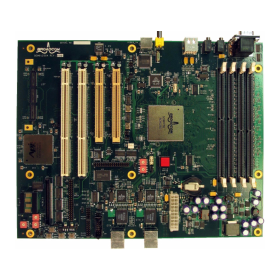
User Manual 05/18/04 Se ction 3: Phy sical Des cription The BCM91250A is implemented in the standard ATX form factor. It is housed in an ATX 2.0 compliant enclosure and ships with a power supply. Figure 3 shows a top view of the BCM91250A. -
Page 13: Block Diagram
User Manual BCM91250A 05/18/04 LOCK IAGRAM Figure 4 shows a block diagram of the BCM91250A. Audio Codec Serial Port S1 Serial Port S0 2x8b HT Connectors 2x64b PCI Slots EJTAG 2x32b PCI Slots HT to PCI 8b HT PCI to USB Bridge... -
Page 14: Connectors
BCM91250A User Manual 05/18/04 ONNECTORS OARD ONNECTORS Figure 5 shows the board and identifies connectors numerically. Compare Figure 5 number callouts with Table 1 for a description of each connector callout. Figure 5: Connector Callouts B roadc om C or por ati on... -
Page 15: Table 1: Connector Descriptions
05/18/04 Table 1 shows BCM91250A connectors. Note: For the nonstandard connectors which have their pins described below you can locate pin 1 on the board by finding the arrow that points to it on the PCB silkscreen. In some cases for connectors with multiple rows and columns of pins, the pin numbers at the corners of the connector are written on the PCB silkscreen. -
Page 16: Pinout For Hypertransport Sockets (J28 And J29)
BCM91250A User Manual 05/18/04 Table 1: Connector Descriptions (Cont.) Board ID Description Dual DB-9 used by UARTs (top = UART 0, bottom = UART 1) Fan (pin 1 = no connect, pin 2 = 12VDC, pin 3 = GND) ROM emulator write line (pin 1 = IO_WR_L, pin 2 = no connect) - Page 17 User Manual BCM91250A 05/18/04 Table 2: Pinout For Hypertransport Sockets (J28 and J29) (Cont.) Odd Pin Even Pin Odd Pin Name Even Pin Name Number Number LDT_RX_CADn6 LDT_TX_CADp2 LDT_RX_CADp6 LDT_TX_CADn2 LDT_RX_CADn5 LDT_TX_CADp3 LDT_RX_CADp5 LDT_TX_CADn3 LDT_RX_CADn4 LDT_TX_CLKp LDT_RX_CADp4 LDT_TX_CLKn LDT_RX_CLKn LDT_TX_CADp4...
-
Page 18: Rom Emulator Pinout
BCM91250A User Manual 05/18/04 ROM E MULATOR INOUT Note: The table layout reflects the physical location of the pins on the connector. Also all I/O signals are 3.3 V outputs that are tolerant of 5V inputs. Table 3: ROM Emulator Pinout... -
Page 19: Ide Connector (J35) Pin 20 Rework
EWORK To use a keyed IDE cable (a cable with pin 20 blocked to prevent incorrect insertion) with the BCM91250A board, you'll need to bend down pin 20. This is easily done with a small flat-head screwdriver after you have located the pin. -
Page 20: Leds
BCM91250A User Manual 05/18/04 Figure 7 shows the positions of the LEDs numerically. Compare Figure 7 number callouts with a description of each LED in Table Figure 7: LED Callouts Table 4: LED Descriptions Board ID Color Description Green PHY 0 Slave indicator... - Page 21 User Manual BCM91250A 05/18/04 Table 4: LED Descriptions (Cont.) Board ID Color Description Green PHY 1 Transmit indicator Green PHY 1 Full Duplex indicator Green PHY 1 Link 1 indicator Green PHY 1 Link 2 indicator Green IDE HDD active indicator...
-
Page 22: Fuses And Battery
BCM91250A User Manual 05/18/04 USES AND ATTERY Figure 8 shows the positions of fuses and the battery alpha-numerically. Compare Figure 8’s alpha-numeric callouts with a description of each component in Table Figure 8: Fuses and Battery Callouts Table 5: Fuses and Battery Descriptions... -
Page 23: Jumpers
User Manual BCM91250A 05/18/04 UMPERS Figure 9 shows the positions of jumpers numerically. Compare Figure 9 number callouts with a description of each jumper in Table Figure 9: Jumper Callouts Table 6: Jumper Descriptions Board ID Function Settings Default System Byte Order... - Page 24 BCM91250A User Manual 05/18/04 Table 6: Jumper Descriptions (Cont.) Board ID Function Settings Default 32-bit PCI clock open = run at slowest PCI agent run at slowest PCI agent select 1-2 = force 33 MHz 2-4 = force 66 MHz...
-
Page 25: Switches
User Manual BCM91250A 05/18/04 WITCHES Figure 10 shows the positions of switches numerically. Compare Figure 10 number callouts with a description of each switch in Table Figure 10: Switch Callouts Table 7: Switch Descriptions Board ID Function Default 16 position rotary switch to set config[5:2] for interpretation by software. - Page 26 BCM91250A User Manual 05/18/04 Table 7: Switch Descriptions (Cont.) Board ID Function Default SW13 Power toggled on or off when pressed B roadc om C or por ati on Page Switches Document 91250A-UM100-R...
-
Page 27: Acceptable Pll Settings
User Manual BCM91250A 05/18/04 PLL S CCEPTABLE ETTINGS Table 8 shows acceptable PLL settings. These settings require a combination of a jumper (J3) and a switch (SW2). Note: The default PLL settings are set according to the speed bin of the BCM1250 part. That setting is the maximum clock speed that the chip can attain without failure. -
Page 28: Peripheral Devices
BCM91250A User Manual 05/18/04 ERIPHERAL EVICES Table 10: SMBus Peripherals SMBus Channel SMBus Address Description 0x2A Maxim MAX6654 temperature sensor DDR SDRAM DIMM SPD EEPROM, MC 0x54 channel 0, slot 0 DDR SDRAM DIMM SPD EEPROM, MC 0x55 channel 0, slot 1... -
Page 29: Supported Dram
User Manual BCM91250A 05/18/04 Table 13: PCI Interrupt Map Interrupt Map Description BCM1250 PCI INTA = PCI connector (J15) INTA 32-bit PCI connector (J15) BCM1250 PCI INTB = PCI connector (J15) INTB BCM1250 PCI INTC = PCI connector (J15) INTC... -
Page 30: Section 4: Firmware Configuration
BCM91250A User Manual 05/18/04 S e c ti o n 4 : F ir m wa r e C o n f ig ur a t i on The firmware image in the flash is bi-endian, so it supports both big and little-endian operation. -
Page 31: Section 5: Troubleshooting
User Manual BCM91250A 05/18/04 Section 5: Troubl eshooting ORRECTIVE ROCEDURES • When CFE is not able to initialize the system and reach the console prompt, the four-character alphanumeric LED display may be used to help debug the initialization sequence. When the Cer2 message appears, a cache error has occurred. -
Page 32: Section 6: Web Resources
266Mhz DDR SDRAM ECC part.aspx?part=MT9VDDT1672AG-265 Xilinx XC9572XL CPLD http://www.xilinx.com/xlnx/xweb/ xil_publications_display.jsp?category=-18744 Hynix HY29LV160 2MB flash memory http://www.hynix.com/datasheet/kor/flash/ detail11.jsp?PartNo=HY29LV160 OPTi Firelink 82C861 USB controller http://www.opti.com/html/usb1394.html Broadcom BCM5421 10/100/ http://www.broadcom.com/products/ 1000BASE-T Gigabit Copper product.php?product_id=BCM5421&cookiecheck=1 Transceiver Samtec connector QSE-060-01-FDA http://www.samtec.com/signal_integrity/ (J28 callout) technical_specifications/overview.asp?series=QSE Samtec connector QTE-060-01-FDA http://www.samtec.com/signal_integrity/... -
Page 33: Bus Interface
User Manual BCM91250A 05/18/04 NTERFACE Table 19: Bus Interface Web Resources Resource Website HyperTransport http://www.hypertransport.org/doc_specifications.htm specification PCMCIA http://www.pcmcia.org/pccardstandard.htm specification JTAG specification http://www.mips.com/content/Documentation/MIPSDocumentation/EJTAG/ doclibrary/ PCI specification http://www.pcisig.com/specifications/conventional/ USB specification http://www.usb.org/developers/docs/ B roadc om C or por ati on Document 91250A-UM100-R Bus Interface... - Page 34 Fax: 949-450-8710 Broadcom Corporation reserves the right to make changes without further notice to any products or data herein to improve reliability, function, or design. Information furnished by Broadcom Corporation is believed to be accurate and reliable. However, Broadcom Corporation does not assume any liability arising out of the application or use of this information, nor the application or use of any product or circuit described herein, neither does it convey any license under its patent rights nor the rights of others.
Need help?
Do you have a question about the BCM91250A and is the answer not in the manual?
Questions and answers