
Related Manuals for Broadcom BCM91250E


Summary of Contents for Broadcom BCM91250E
- Page 1 USER MANUAL BCM91250E Evaluation Board 91250E-UM100-R 16215 Alton Parkway • P.O. Box 57013 • Irvine, CA 92619-7013 • Phone: 949-450-8700 • Fax: 949-450-8710 01/07/05...
- Page 2 All rights reserved Printed in the U.S.A. ® Broadcom and the pulse logo are trademarks of Broadcom Corporation and/or its subsidiaries in the United States and certain other countries. All other trademarks mentioned are the property of their respective owners.
-
Page 3: Table Of Contents
User Manual BCM91250E 01/07/05 ABLE OF ONTENTS Section 1: Product Overview ....................1 Introduction ..............................1 Items Included with the Shipment ......................1 Features ................................ 1 Hardware ..............................1 Firmware ..............................1 Section 2: Getting Started....................3 Section 3: Physical Description ..................5 Block Diagram .............................. - Page 4 BCM91250E User Manual 01/07/05 IST OF ABLES Table 1: Connector Descriptions......................... 6 Table 2: Pinout For Hypertransport Socket (J3) ....................7 Table 3: Pinout For Mezzanine Connector (J17) ....................9 Table 4: ROM Emulator Pinout .........................11 Table 5: LED Descriptions ..........................13 Table 6: Fuses and Battery Descriptions ......................14...
- Page 5 User Manual BCM91250E 01/07/05 IST OF IGURES Figure 1: BCM91250E Front View........................5 Figure 2: BCM91250E Block Diagram........................ 5 Figure 3: Connector Callouts..........................6 Figure 4: LED Callouts ............................. 12 Figure 5: Fuses and Battery Callouts ....................... 14 Figure 6: Switch Callouts..........................15...
- Page 6 BCM91250E User Manual 01/07/05 Bro adco m C orp or atio n Page vi Document 91250E-UM100-R...
-
Page 7: Section 1: Product Overview
The BCM91250E evaluation board is an evaluation platform intended to support the needs of prospective users of the BCM1250 processor. This user manual provides information on how to get the BCM91250E evaluation board up and running quickly. This manual also describes how to locate, configure, and observe the various connectors, switches, jumpers, and LEDs on the BCM91250E, allowing software development and evaluation of the BCM1250 processor to begin. - Page 8 There are many parameters configurable at build time that can be used to customize CFE to suit diverse customer requirements. On the BCM91250E, CFE can load programs (such as S-records, raw binary, or ELF formatted) from bootstrap devices in a variety of ways, including: •...
-
Page 9: Section 2: Getting Started
Complete the following steps to get to a BCM91250E CFE (firmware) prompt. Connect a 9-pin null modem cable to the serial port of the BCM91250E and to a serial port on a workstation/PC. Use a terminal program and set it to 115200 bps, 8-bit data, 1-stop bit, no parity, and no flow control. - Page 10 BCM91250E User Manual 01/07/05 c. To run a program, type the following: boot -elf tftp_server:/path_to_software/program B roadc om C or por ati on Page 4 Getting Started Document 91250E-UM100-R...
-
Page 11: Section 3: Physical Description
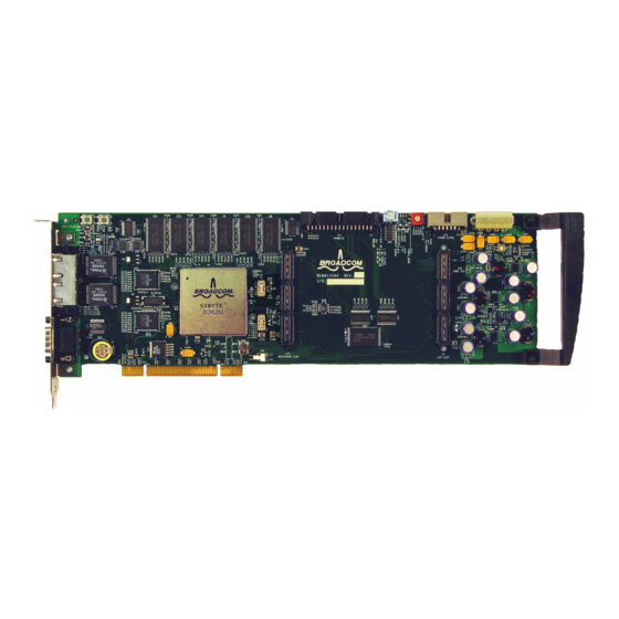
User Manual BCM91250E 01/07/05 Se ction 3: Phy sical Des cription The BCM91250E is implemented in the standard full length PCI card form factor. Figure 1 shows a front view of the BCM91250E. Figure 1: BCM91250E Front View LOCK IAGRAM Figure 2 shows a block diagram of the BCM91250E. -
Page 12: Table 1: Connector Descriptions
Figure 3 shows the board and identifies connectors numerically. For a description of each connector callout, compare Figure 3’s number callouts with Table 1. Figure 3: Connector Callouts The following table shows the BCM91250E connectors. Table 1: Connector Descriptions Board ID Description Dual-sided 62-pin edge finger PCI connector. -
Page 13: Pinout For Hypertransport Socket (J3)
User Manual BCM91250E 01/07/05 (J3) INOUT YPERTRANSPORT OCKET Note: The table layout reflects the physical location of the pins on the connector. The middle pins (121-132) are not shown though since they are all connected to ground (GND). More information about these connectors can be found in “Web Resources” on page 19. - Page 14 BCM91250E User Manual 01/07/05 Table 2: Pinout For Hypertransport Socket (J3) (Cont.) Odd Pin Even Pin Odd Pin Name Even Pin Name Number Number LDT_RX_CLKn LDT_TX_CADp4 LDT_RX_CLKp LDT_TX_CADn4 LDT_RX_CADn3 LDT_TX_CADp5 LDT_RX_CADp3 LDT_TX_CADn5 LDT_RX_CADn2 LDT_TX_CADp6 LDT_RX_CADp2 LDT_TX_CADn6 LDT_RX_CADn1 LDT_TX_CADp7 LDT_RX_CADp1 LDT_TX_CADn7...
-
Page 15: Pinout For Mezzanine Connector (J17)
User Manual BCM91250E 01/07/05 (J17) INOUT EZZANINE ONNECTOR Note: The table layout reflects the physical location of the pins on the connector. The middle pins (121-132) are not shown though since they are all connected to ground (GND). More information about these connectors can be found in “Web Resources” on page 19. - Page 16 BCM91250E User Manual 01/07/05 Table 3: Pinout For Mezzanine Connector (J17) (Cont.) Odd Pin Even Pin Odd Pin Name Even Pin Name Number Number E2_MDIO REFCLK02 IO_RD_WR GPIO15 IO_CS_L3 GPIO14 IO_CS_L4 GPIO13 IO_ALE GPIO12 GPIO11 S1_DIN GPIO10 S1_DIN_RCLKIN GPIO9 S1_CTS_TCLKIN...
-
Page 17: Rom Emulator Pinout
User Manual BCM91250E 01/07/05 ROM E MULATOR INOUT Note: The table layout reflects the physical location of the pins on the connector. Also all I/O signals are 3.3 V outputs that are tolerant of 5V inputs. Table 4: ROM Emulator Pinout... -
Page 18: Leds
BCM91250E User Manual 01/07/05 Figure 4 shows the positions of the LEDs numerically. Compare Figure 4’s number callouts with a description of each LED in Table 5 on page 13. Figure 4: LED Callouts B roadc om C or por ati on... -
Page 19: Table 5: Led Descriptions
User Manual BCM91250E 01/07/05 Table 5: LED Descriptions Board ID Color Description 2.5V Fuse blown indicator 3.3V Fuse blown indicator D7 * Ethernet Port E1 PHY LEDs Link2 = Speed indicator. Green Link1 = Speed indicator. Yellow Fdx = Full-duplex indicator. -
Page 20: Fuses And Battery
BCM91250E User Manual 01/07/05 USES AND ATTERY Figure 5 shows the positions of the fuses and battery alpha-numerically. Compare Figure 5’s alpha-numeric callouts with a description of each fuse or battery in Table 6. Figure 5: Fuses and Battery Callouts... -
Page 21: Switches
User Manual BCM91250E 01/07/05 WITCHES Figure 6 shows the positions of switches numerically. Compare Figure 6’s number callouts with a description of each switch in Table 7. Figure 6: Switch Callouts Table 7: Switch Descriptions Board ID Function Default 16 position rotary switch to set config[5:2] for interpretation by software. -
Page 22: Peripheral Devices
BCM91250E User Manual 01/07/05 ERIPHERAL EVICES Table 8: SMBus Peripherals SMBus Channel SMBus Address Description 0x2A Maxim MAX6654 temperature sensor. 0x50 Microchip 28LC128 EEPROM. 0x68 ST Microelectronics M41T81 RTC. Table 9: Generic Bus Peripherals Chip Select # Description Hynix HY29LV160 boot flash memory or ROM Emulator (depending on SW4 setting) -
Page 23: Section 4: Firmware Configuration
User Manual BCM91250E 01/07/05 S e c ti o n 4 : F ir m wa r e C o n f ig ur a t i on The firmware image in the flash is bi-endian, so it supports both big and little-endian operation. The following table describes where and how much physical memory the firmware maps to the chip selects on the generic bus. -
Page 24: Section 5: Troubleshooting
BCM91250E User Manual 01/07/05 Section 5: Troubl eshooting ORRECTIVE ROCEDURES When CFE is not able to initialize the system and reach the console prompt, output on the serial boot console may be used to help debug the initialization sequence. When the Cer2 message appears, a cache error has occurred. -
Page 25: Section 6: Web Resources
User Manual BCM91250E 01/07/05 Section 6: Web Res ource s Table 15: SiByte Web Resources Resource Website BCM1250 and BCM1125H User Manual http://sibyte.broadcom.com/public/resources/ SB-1 Core User Manual General information http://sibyte.broadcom.com/public/ ERIPHERAL OMPONENTS Table 16: Peripheral Component Web Resources Board Description... - Page 26 Fax: 949-450-8710 Broadcom Corporation reserves the right to make changes without further notice to any products or data herein to improve reliability, function, or design. Information furnished by Broadcom Corporation is believed to be accurate and reliable. However, Broadcom Corporation does not assume any liability arising out of the application or use of this information, nor the application or use of any product or circuit described herein, neither does it convey any license under its patent rights nor the rights of others.
Need help?
Do you have a question about the BCM91250E and is the answer not in the manual?
Questions and answers