Chapters
Table of Contents
Troubleshooting

Subscribe to Our Youtube Channel
Related Manuals for Fluke 6080A


Summary of Contents for Fluke 6080A
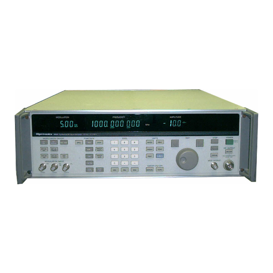
- Page 1 ® Advanced Test Equipment Rentals www.atecorp.com 800-404-ATEC (2832) 6080A/AN SYNTHESIZED SIGNAL GENERATOR Service Manual P/N 868906 October 1989 PO Box C9090 Everett WA 98206 ©1989, John Fluke Mfg. Co. Inc. All rights reserved...
- Page 2 In the event of failure of a product covered by this warranty, JOHN FLUKE MFG. CO., INC will repair and calibrate an instrument returned to an authorized Service Center within 2 years of the original purchase;...
-
Page 3: Table Of Contents
Table of Contents SECTION TITLE PAGE INTRODUCTION AND SPECIFICATIONS 1-1. INTRODUCTION 1-2. UNPACKING THE SIGNAL GENERATOR 1-3. SAFETY 1-4. ACCESSORIES 1-5. SIGNAL GENERATOR SPECIFICATIONS THEORY OF OPERATION 2-1. INTRODUCTION 2-2. GENERAL DESCRIPTION 2-3. Front Panel Section 2-4. Upper/Lower Module Sections 2-5. -
Page 4: Title Page
TABLE OF CONTENTS, continued SECTION TITLE PAGE 3-8. FM CALIBRATION 3-9. Front Panel FM Calibration Procedure 3-10. Remote FM Calibration 3-11. RF LEVEL CALIBRATION 3-10 3-12. Front Panel Level Calibration Procedure 3-11 3-13. Remote Level Calibration Procedure 3-13 3-14. REFERENCE OSCILLATOR CALIBRATION 3-14 3-15. - Page 5 TABLE OF CONTENTS, continued SECTION TITLE PAGE CIRCUIT DESCRIPTIONS, TROUBLESHOOTING, AND ALIGNMENT 6-1. INTRODUCTION 6-2. MODULE REPLACEMENT 6-3. Display PCA 6-4. A2 Coarse Loop PCA 6-5. A3 Sub-Synthesizer PCA 6-6. A4 Sub-Synthesizer PCA 6-7. A5 Coarse Loop VCO PCA 6-8. A6 Mod Oscillator PCA 6-9.
- Page 6 TABLE OF CONTENTS, continued SECTION TITLE PAGE DIGITAL CONTROLLER 6B-1 6B-1. DIGITAL CONTROLLER BLOCK DIAGRAM 6B-1 6B-2. DIGITAL CONTROLLER CIRCUIT DESCRIPTION (A13) 6B-1 6B-3. Microprocessor 6B-1 6B-4. Memory 6B-1 6B-5. Memory Control 6B-3 6B-6. Front Panel Interface 6B-3 6B-7. IEEE-488 Interface 6B-3 6B-8.
- Page 7 TABLE OF CONTENTS, continued SECTION TITLE PAGE 6C-11. SUB-SYNTHESIZER VCO (A3) CIRCUIT DESCRIPTION 6C-16 6C-12. SUB-SYNTHESIZER VCO TROUBLESHOOTING 6C-16 6C-13. COARSE LOOP CIRCUIT DESCRIPTION (A2) 6C-17 6C-14. REFERENCE SECTION BLOCK DIAGRAM 6C-17 6C-15. COARSE LOOP BLOCK DIAGRAM 6C-20 6C-16. COARSE LOOP TROUBLESHOOTING 6C-22 6C-17.
- Page 8 TABLE OF CONTENTS, continued SECTION TITLE PAGE 6D-18. Output PCA Het Mixer Level Adjustment, R72 6D-16 6D-19. Output PCA Het Level Adjustment, 6D-17 6D-20. Premodulator PCA Bandwidth Adjustment, R51 and C7 6D-17 6D-21. Output PCA Q16 Bias Adjustment, R96 6D-18 6D-22.
- Page 9 TABLE OF CONTENTS, continued SECTION TITLE PAGE SCHEMATIC DIAGRAMS TABLE OF CONTENTS APPENDICES INSTRUMENT PRESET STATE SPECIAL FUNCTION TABLE REJECTED ENTRY ERROR CODES OVERRANGE/UNCAL STATUS CODES SELF-TEST STATUS CODES COMPENSATION MEMORY STATUS CODES EXAMPLE CALIBRATION CONTROLLER PROGRAMS COMPENSATION PROCEDURES REAR PANEL AUX CONNECTOR PINOUT viilviii...
- Page 11 TABLE TITLE PAGE 1-1. Accessories Included with each Signal Generator 1-2. Optional Accessories 1-3. 6080A/AN Specifications 1-4. Typical Signal Generator Performance 2-1. Frequency Coverage Bands 3-1. Front Panel Controls for AM Calibration Procedure 3-2. Remote Programming Commands for AM Calibration Procedure 3-3.
- Page 12 LIST OF TABLES, continued TABLE TITLE PAGE 6A-1. Supplies Provided by Power Supply Assembly 6A-3 6C-1. Sub-Synthesizer PCA Test Points 6C-11 6C-2. A3 Sub-Synthesizer VCO PCA DC Voltages 6C-17 6C-3. Coarse Loop RF Voltage Levels 6C-24 6C-4. N-Divider Logic States 6C-25 6C-5.
- Page 13 List of Illustrations FIGURE TITLE PAGE 3-1. Basic Structure of Calibration Program 3-2. Structure of the AM Calibration Program 3-3. Basic Structure of FM Calibration Program 3-4. Basic Structure of Level Calibration Program 3-13 3-5. Basic Structure of the Reference Oscillator Calibration Program 3-16 4-1.
-
Page 15: Introduction And Specifications
RF components and systems including filters, amplifiers, mixers, and radios, particularly off-channel radio testing. Specifications of the 6080A/AN are provided at the end of this section. The salient features of the 6080A/AN are as follows: •... -
Page 16: Safety
0 to 50° C without degradation of its safety. WARNING TO AVOID ELECTRIC SHOCK, USE A POWER CORD THAT HAS A THREE-PRONG PLUG. IF THE PROPER POWER CORD IS NOT USED, THE 6080A/AN CASE CAN DEVELOP AN ELECTRICAL POTENTIAL ABOVE EARTH GROUND. WARNING PIVOTING MODULE INSTRUCTIONS... -
Page 17: Accessories
The accessories and manuals included with each signal generator are listed in Table 1-1. The optional accessories available are listed in Table 1-2. SIGNAL GENERATOR SPECIFICATIONS 1 -5. Table 1-3 lists the 6080A/AN specifications. Table 1-4 lists typical performance characteristics. Table 1-1. Accessories Included with each Signal Generator DESCRIPTION... - Page 18 INTRODUCTION AND SPECIFICATIONS Table 1-3. 6080A/AN Specifications NOTE Unless otherwise noted, the following performance is guaranteed over the specified environmental and AC power line conditions two hours after turn-on. FREQUENCY (10-DIGIT DISPLAY) RANGE 0.50 to 1024 MHz in 7 bands: BAND .50-15 MHz...
- Page 19 INTRODUCTION AND SPECIFICATIONS Table 1-3. 6080A/AN Specifications (cont) SPECTRAL PURITY (CW ONLY) NON-HARMONIC SPURIOUS < -100 dBc for offsets greater than 15 kHz. NOTE Fixed frequency spurs are <-100 dBc or < -140 dBm, whichever is larger. NOTE dBc refers to decibels relative to the carrier frequency, or in this case, relative to the signal level.
- Page 20 INTRODUCTION AND SPECIFICATIONS Table 1-3. 6080A/AN Specifications (cont) DEVIATION RF Frequency (rates = .1, 1, 50 kHz) 0 to 1 kHz min Frequency < 1 MHz 0 to 10 kHz min 1 MHz < Frequency < 32 MHz 0 to 100 kHz mln 32 MHz <...
- Page 21 INTRODUCTION AND SPECIFICATIONS Table 1-3. 6080A/AN Specifications (cont) IEEE-488 INTERFACE FUNCTIONS SH1, AH1, T5, TE0, L3, LEO, SR1, RL1, PRO, DC1, DT1, C0, and E2. Complies with IEEE Std. 488.1-1987 and 488.2-1987. INTERNAL MODULATION SOURCE SINE WAVE 10 Hz to 100 kHz synthesized sine wave.
- Page 22 INTRODUCTION AND SPECIFICATIONS Table 1-3. 6080A/AN Specifications (cont) ELECTROMAGNETIC COMPATIBILITY.. The radiated emissions induce < 1 μV into a 1-inch diameter, 2-turn loop, 1-inch from any surface as measured into a 50-ohm receiver. COMPLIES WITH THE FOLLOWING STANDARDS: CE03 of MIL-STD-461B (Power and interconnecting leads), 0.015 to 50 MHz.
- Page 23 INTRODUCTION AND SPECIFICATIONS Table 1-4. Typical Signal Generator Performance FREQUENCY (10-DIGIT DISPLAY) RANGE 0.01 to 1056 MHz in 7 bands: BAND .01-15 MHz 0.01 to 14.999999 MHz, BAND 15-32 MHz ......15 to 31.999999 MHz, 32 to 63.999999 MHz, BAND 32-64 MHz BAND 64-128 MHz...
- Page 24 INTRODUCTION AND SPECIFICATIONS Table 1-4. Typical Signal Generator Performance (cont) ± 2 dB from +19 to -100 dBm and for F from 0.01 to 0.4 MHz. ± 3 dB from -100 to -127 dBm and for F from 0.01 to 0.4 MHz.
- Page 25 INTRODUCTION AND SPECIFICATIONS Table 1-4. Typical Signal Generator Performance (cont) < -136 dBc/Hz @ 20 kHz offset @ Frequency = 1 GHz < -140 dBc/Hz @ 20 kHz offset @ Frequency = 500 MHz BROADBAND SSB PHASE NOISE FLOOR < -140 dBc/Hz @ 100 kHz offset @ +13 dBm. RESIDUAL AM (in 0.05- to 15-kHz Band) <...
- Page 26 INTRODUCTION AND SPECIFICATIONS Table 1-4. Typical Signal Generator Performance (cont) Minimum FM rate at max deviation in any band, ACFM mode is 60 Hz. @ 1/2 max deviation..30 Hz @ 1/4 max deviation..15 Hz from 1/4 to 1/64 max deviation..15 Hz @ 1/64 max deviation..
- Page 27 INTRODUCTION AND SPECIFICATIONS Table 1-4. Typical Signal Generator Performance (cont) ±10mV MAX DC INPUT INCIDENTAL AM < 1 % AM @ 1 kHz rate and < 10 kHz dev NOTE FM specific ations apply where: RF Frequency - Deviation > 150 kHz RF Frequency - Mod Rate >...
- Page 28 INTRODUCTION AND SPECIFICATIONS Table 1-4. Typical Signal Generator Performance (cont) HIGH RATE PHASE MODULATION... ACPM 20 Hz to 100 kHz BANDWIDTH (3 dB) DCPM DC to 100 kHz (Access by SPCL 721) NOTE Phase Modulation specs are valid where RF Frequency - Modulation Frequency > 150 kHz PULSE MODULATION (RF FREQUENCIES FROM 10 TO 1056 MHz) ON/OFF RATIO 40 dB minimum for frequencies from 100to 1056 MHz...
- Page 29 INTRODUCTION AND SPECIFICATIONS Table 1-4. Typical Signal Generator Performance (cont) TRIP/RESET Flashing RF OFF annunciator indicates a tripped condition. Pushing RF ON/OFF button will reset signal generator. IEEE-488 INTERFACE FUNCTIONS SH1, AH1, T5, TE0, L3, LE0, SR1, RL1, PP0, DC1, DT1, C0, and E2.
- Page 30 INTRODUCTION AND SPECIFICATIONS Table 1-4. Typical Signal Generator Performance (cont) SWEEP FUNCTIONS Symmetrical sweep, Asymmetrical sweep, Sweep speed DATA ENTRY PARAMETERS Sweep width and sweep increment SWEEP SPEED Minimum 40 ms per increment selectable as (mini- mum + dwell time) where dwell time can be 0, 20, 50, 100, 200, or 500 ms at each increment.
- Page 31 INTRODUCTION AND SPECIFICATIONS Table 1-4. Typical Signal Generator Performance (cont) ELECTROMAGNETIC COMPATIBILITY.. The radiated emissions induce < 1 μV into a 1-inch diameter, 2-turn loop, 1-inch from any surface as measured into a 50-ohm receiver. COMPLIES WITH THE FOLLOWING STANDARDS: CE03 of MIL-STD-461B (Power and interconnecting leads), 0.015 to 50 MHz.
- Page 32 INTRODUCTION AND SPECIFICATIONS Table 1-4. Typical Signal Generator Performance (cont) DCFM DRIFT 3 ppm/hr for < 1/16 max deviation (after 2 hour warmup and at constant 8 ppm/hr for > 1/16 max deviation temperature) 1-18...
-
Page 33: Theory Of Operation
Section 2 Theory of Operation INTRODUCTION 2-1. Section 2 of this manual provides a basic description of the 6080A/AN Synthesized Signal Generator (also referred to throughout as the "signal generator"). Three major topics are covered: • General Description Briefly explains the functions and components of the four major sections of the Generator. -
Page 34: Front Panel Section
THEORY OF OPERATION Front Panel Section 2-3. The front panel section of the signal generator provides the operator interface, including the primary controls, connectors, and indicators. All front panel keys and displays (except the power switch that directly controls the power supply) are monitored and handled by the A13 Controller PCA, which is located in the output module section. -
Page 35: Frequency Coverage Bands
THEORY OF OPERATION Table 2-1. Frequency Coverage Bands BAND FREQUENCY COVERAGE 0.01 to 14.999999 MHz Divide-by-32 15 to 31.999999 MHz Divide-by-16 32 to 63.999999 MHz Divide-by-8 64 to 127.999999 MHz Divide-by-4 128 to 255.999999 MHz Divide-by-2 256 to 511.999999 MHz Fundamental 512 to 1056 MHz Three signals are combined in the sum loop to produce a signal that ranges from 480 to... - Page 36 THEORY OF OPERATION Frequency Modulation 2-8. Frequency modulation (FM) is programmable with three digits of resolution in six ranges. The deviation is programmed using the 12-bit FM DAC and three FM range bits. The FM DAC and range settings are dependent on the programmed deviation and the RF output frequency.
- Page 37 THEORY OF OPERATION Output/Level Control 2-10. Level control is provided by two separate circuits: a step attenuator and a vernier level DAC. The A20 Attenuator/RPP Assembly provides coarse level control in 6.02-dB steps. Fine level control is provided by a vernier level DAC that varies the leveling-loop control voltage.
-
Page 38: Power Supply Description
The modulation oscillator is made up of two sections; a periodic wave generator and a pulse generator. Both functions are implemented in a custom integrated circuit and are synthesized from the main reference frequency source of the 6080A/AN. The periodic wave generator frequency can be set from 0.1 Hz to 200 kHz with resolution of 0.1 Hz. -
Page 39: Calibration/Compensation Memory
THEORY OF OPERATION The diagnostic service task monitors the instrument status signals. The front panel key task, knob task and IEEE-488 task process user input. A fifth task controls the RF output when a frequency or amplitude sweep is active. A sixth task is activated only when needed to process certain STATUS (out-of-range or malfunction) or REJ ENTRY (rejected entry) conditions that cause the display to flash. -
Page 41: Closed-Case Calibration
The calibration procedures can be performed at the specified 2-year calibration intervals or whenever one wishes to optimize the performance of the 6080A/AN Synthesized Signal Generator. The procedures can be performed from the front panel or remotely under the control of an IEEE-488 bus controller. -
Page 42: Front Panel Calibration
The basic structure of a calibration program is shown in Figure 3-1. Initiate 6080A/AN calibration procedure Initialize measurement equipment Loop Ask 6080A/AN for RF frequency Exit loop if frequency is special end code "9E+09" Get reading from measurement equipment Send reading the 6080A/AN... -
Page 43: Calibration Data
When the switch is in the 0 (OFF) position, the data is write protected in hardware. The calibration data can be generated in one of two ways: by the Fluke factory or by the user. Each calibration data segment contains a data origin tag which specifies how the data was created. -
Page 44: Am Calibration
The AM calibration procedures allow a single point calibration of the AM depth to be performed. An RF modulation meter is connected to the 6080A/AN's RF output and the AM calibration factor is adjusted based on the meter reading. The procedure specific parameters are as follows: Adjustment Range: ±5% AM Depth... -
Page 45: Front Panel Controls For Am Calibration Procedure
CLOSED-CASE CALIBRATION 4. Select the peak+ mode, enable the 50-Hz high-pass filter, and enable the 3 kHz low-pass filter on the modulation meter. 5. Use the edit knob to change the adjustment value until the modulation meter reads 50.0%. 6. Press twice to store the new data. -
Page 46: Remote Am Calibration Procedure
The controller program must ensure that each mod meter reading is settled before sending the reading to the 6080A/AN. The program listing in Appendix G uses a simple but effective method to obtain valid mod meter readings. -
Page 47: Fm Calibration
The FM calibration procedures allow a single point calibration of the FM deviation to be performed. An RF modulation meter is connected to the 6080A/AN's RF output, and the FM calibration factor is adjusted based on the meter reading. The procedure specific parameters are as follows: Adjustment Range: ±... -
Page 48: Front Panel Fm Calibration Procedure
CLOSED-CASE CALIBRATION Front Panel FM Calibration Procedure 3-9. The front panel FM calibration procedure is initiated by the following key sequence: The display is reconfigured for the procedure. Several of the front panel controls are disabled or operate differently than they normally do. Table 3-3. shows all of the active controls and describes their function while performing the front panel FM calibration procedure. -
Page 49: Remote Fm Calibration
Refer to the heading "Remote Calibration" (earlier in Section 3) for general information relating to all remote calibration procedures. A complete program listing that runs on a Fluke 1722A controller is provided in Appendix G. The basic structure of the FM calibration program is shown in Figure 3-3. -
Page 50: Rf Level Calibration
The controller program must ensure that each mod meter reading is settled before sending it to the 6080A/AN. The program listing in Appendix G uses a simple but effective method to obtain valid mod meter readings. -
Page 51: Front Panel Level Calibration Procedure
CLOSED-CASE CALIBRATION The front panel display is reconfigured during the procedures. The target level is displayed in the modulation field, the RF frequency is displayed in the frequency field, the adjustment value is displayed in the amplitude field, and the CAL annunciator is lit. -
Page 52: Front Panel Controls For Level Calibration Procedure
CLOSED-CASE CALIBRATION Table 3-5. Front Panel Controls for Level Calibration Procedure CONTROLS FUNCTION AND DESCRIPTION Bright-Digit Editing KNOB Turn the edit knob to adjust the level calibration factor. Use the left/right arrow keys to move the bright-digit within the adjustment field. The bright-digit is always located in the adjustment field. -
Page 53: Remote Level Calibration Procedure
Refer to the heading "Remote Calibration" (earlier in Section 3) for general information relating to all remote calibration procedures. A complete program listing that runs on a Fluke 1722A controller is provided in Appendix G. The basic structure of the level calibration program is shown in Figure 3-4. -
Page 54: Reference Oscillator Calibration
The reference oscillator calibration procedures allow a single-point calibration of the internal 10-MHz reference oscillator to be performed. A frequency counter is connected to the 6080A/AN's RF output, and the reference oscillator calibration factor is adjusted based on the counter reading. The procedure specific parameters are... -
Page 55: Front Panel Reference Oscillator Calibration Procedure
CLOSED-CASE CALIBRATION NOTE The rear panel CAL|COMP switch must be set to the 1 (on) position before initiating the calibration procedures. Front Panel Reference Oscillator Calibration Procedure 3-15. The front panel reference oscillator calibration procedure is initiated by the following key sequence: The display is reconfigured for the procedure. -
Page 56: Remote Reference Oscillator Calibration Procedure
(earlier in Section 3) for general information relating to all remote calibration procedures. A complete program listing that runs on a Fluke 1722A controller is provided in Appendix G. The basic structure of the level calibration program is shown in Figure 3-5. -
Page 57: Remote Programming Commands For Reference Oscillator Calibration Procedure
Table 3-8. Remote Programming Commands for Reference Oscillator Calibration Procedure COMMANDS DESCRIPTION CAL_REFOSC Initiate the remote reference oscillator calibration procedure CC_RDFREQ Send the counter meter to the 6080A/AN CC_FREQ? Request the RF frequency CC_TARGET? Request the target value RFOUT Program the RF output on/off... -
Page 59: Performance Tests
INTRODUCTION 4-1. The information in the Section 4 describes the performance tests for the key parameters of the 6080A/AN Synthesized Signal Generator (also referred to throughout as the "signal generator"). Instrument specifications are used as the performance standard. These closed-case performance tests may be used as: •... - Page 60 0.1 to 2100 MHz VSWR < 1.15 Narda 777C LF Synthesized Signal 10 Hz to 11 MHz, 10 Hz steps, 6011A Generator 1V peak, Spurs and Harm < -50 dB 6080A/AN HF Synthesized 0.5 to 1024 MHz Sig-Gen (Low Residual)
- Page 61 PERFORMANCE TESTS Table 4-1. Recommended Test Equipment (cont) MANUFACTURER INSTRUMENT NAME MINIMUM REQUIREMENT NOTES DESIGNATION Frequency Standard House Standard, 10 MHz Test Cable Dual pin to BNC 732891 Adapter, Coax 50-ohm, Type-N(m) to BNC(f) Y9308 A,P,T Adapter, Service 50-ohm, Module output to SMA 744177 Two-Turn Loop For Leakage test (See Figure 4-1)
-
Page 62: Power-On Test
PERFORMANCE TESTS Figure 4-1. Two-Turn Loop POWER-ON TEST 4-3. This performance test is the built-in self-test that performs a simple functional check of the instrument. REQUIREMENT: The signal generator successfully passes the self-test. REMARKS: The test is begun each time the signal generator is turned on. Press any of the FUNCTION keys or the key to abort the test. -
Page 63: Frequency Accuracy Test
PERFORMANCE TESTS FREQUENCY ACCURACY TEST 4-4. The internal time base is compared to that of a Frequency Standard. REQUIREMENTS: The frequency of the UUT time base is within the specified limits. TEST EQUIPMENT: • Frequency standard • Frequency counter PROCEDURE: 1. -
Page 64: High-Level Accuracy Test
UUT. NOTE To test attenuator sections 4 through 7, program the 6080A/AN Signal Generator to -12 dBm, and key in through , respectively. -
Page 65: High-Level Accuracy Test Conditions
Table 4-3 shows the parameters of the high-level accuracy test. NOTE To test attenuator sections 4 through 7, program the 6080A/AN Signal Generator to -12 dBm, and key in through... -
Page 66: Mid-Level Accuracy Test
PERFORMANCE TESTS 8. Repeat steps 4 through 7 with the UUT programmed to each of the following frequencies: 14, 20, 40, 80, 160, 320, 550, 640, 700, 850, 950, 1024 MHz Table 4-3 is an example of this procedure in which the measured power and the error calculations are shown. -
Page 67: Low-Level Accuracy Test
PERFORMANCE TESTS If the UUT fails this test after passing the high level accuracy test, problems with the A21 Attenuator PCA or the A7 Relay Driver PCA are indicated. It is convenient to use the UUT RF ON/OFF control when zeroing the power meter. PROCEDURE: 1. -
Page 68: Alternate-Level Accuracy Test
PERFORMANCE TESTS It is convenient to use the UUT RF ON/OFF control when zeroing the power meter. PROCEDURE: 1. Program the UUT to SPCL 909, 10 MHz, and -67 dBm. Calibrate, then connect the power meter with a low-level power sensor to the UUT RF OUTPUT. - Page 69 PERFORMANCE TESTS REMARKS: This test is a more comprehensive test then the high-level, mid-level, and low-level accuracy tests. If the UUT fails this test, the UUT needs to be calibrated (Section 3) or repaired (Section 6). If the UUT fails this test at higher levels, problems with the A8 Output PCA, the A21 Attenuator PCA, the A7 Relay Driver PCA may be indicated.
- Page 70 PERFORMANCE TESTS NOTE When the Recal annunciator on the measurement receiver lights while stepping through UUT levels, press the CALIBRATE button on the measuring receiver and wait for a stable reading. 8. Repeat steps 4 through 7 for each of the following UUT frequencies: 14, 20, 40, 80, 160, 320, 550, 640, 700, 850, 950, and 1024 MHz Figure 4-2.
-
Page 71: Flatness Test
PERFORMANCE TESTS FLATNESS TEST 4-10. A power meter and sensor are used to verify the high level flatness of the instrument. REQUIREMENT: Amplifier flatness is: < ± 1 dB at +10 dBm over the frequency range of 0.5 to 1024 MHz. TEST EQUIPMENT: •... -
Page 72: Output Leakage Test
PERFORMANCE TESTS OUTPUT LEAKAGE TEST 4-11. The output signal leakage is verified using a 1-inch diameter, two-turn loop. The induced signal is measured with an RF Spectrum Analyzer and compared to a l-μV reference established at each reference frequency. The two-turn loop must be 1 inch away from any surface of the UUT. -
Page 73: Harmonic And Line-Related Spurious Test
PERFORMANCE TESTS HARMONIC AND LINE-RELATED SPURIOUS TEST 4-12. The Harmonic and Line-Related Spurious Test uses an RF spectrum analyzer to compare the level of the harmonic signal and close-in spurious signals to the desired signal at various programmed frequencies. REQUIREMENTS: •... -
Page 74: Phase Noise And Non-Harmonic Spurious Tests
PERFORMANCE TESTS PHASE NOISE AND NON-HARMONIC SPURIOUS TESTS 4-13. The Phase Noise test uses a phase noise measurement system and a low phase noise reference signal generator to measure the UUT phase noise. Non-harmonic spurious signals are measured with the phase noise measurement system and low phase noise reference signal generator and are verified with an RF spectrum analyzer. -
Page 75: Modulation Tests
PERFORMANCE TESTS MODULATION TESTS 4-14. The following tests use a modulation analyzer to verify modulation accuracy and residual and incidental modulation of the UUT. The modulation distortion is verified by measuring the demodulated output of the modulation analyzer with a distortion analyzer. - Page 76 PERFORMANCE TESTS NOTE The following procedures must be performed in the order described below to ensure that the proper equipment is connected and appropriate programs are enabled. PROCEDURE: 1. Internal Modulation Oscillator Frequency Test a. Connect the UUT MODULATION OUTPUT to the frequency counter input. b.
-
Page 77: Am Test Conditions
PERFORMANCE TESTS e. Set the distortion analyzer to measure the total harmonic distortion (THD) of the 1-kHz modulation signal. f. Verify that the THD is less than 5%. g. Program the remaining combinations of RF frequency, level, and AM depth listed in Table 4-5. - Page 78 PERFORMANCE TESTS 4. AM Bandwidth Test a. Program the UUT for 50% INT AM at 1 kHz rate at 100 MHz, and -2 dBm. b. With the modulation analyzer reading AM%, press the RATIO DB key to normalize the reading to 0.0 dB. c.
- Page 79 PERFORMANCE TESTS d. Set the distortion analyzer to measure distortion at 1 kHz. e. Verify that the modulation analyzer reading is between 19 and 21 kHz, and that the THD is less than 2%. Repeat at deviations of 5 and 10 kHz. Verify that the modulation analyzer reading is within ±...
- Page 80 PERFORMANCE TESTS b. Program the UUT to SPCL 909, EXT øM, and 10 radians phase deviation. c. Program the LFSSG for .3 kHz and .7071V RMS, as measured by the DVM. d. Program the modulation analyzer to measure øM + peak in a 50-Hz to 15-kHz bandwidth.
-
Page 81: Voltage Standing-Wave Ratio (Vswr) Tests
PERFORMANCE TESTS VOLTAGE STANDING-WAVE RATIO (VSWR) TESTS 4-15. The Voltage Standing-Wave ratio (VSWR) tests use a VSWR bridge and a spectrum analyzer to verify VSWR of the UUT. REQUIREMENTS: The output VSWR is less than 1.5:1 for output levels < -10 dBm; < 2.5:1 elsewhere. EQUIPMENT REQUIRED: •... -
Page 82: Pulse Tests
PERFORMANCE TESTS g. Connect the HFSSG to the RF IN port of the VSWR Bridge, h. Program the HFSSG to 10 MHz at +13 dBm. Set the RF spectrum analyzer to display approximately 10 to 1024 MHz and set the reference level to +10 dBm. Step the HFSSG from 10 to 1024 MHz in 10-MHz steps. - Page 83 PERFORMANCE TESTS NOTE The following procedures must be performed in the order described below to ensure that the proper equipment is connected and appropriate programs are enabled. PROCEDURE: 1. Static Test a. Program the UUT to 1024 MHz and +10 dBm. b.
- Page 84 PERFORMANCE TESTS Repeat steps f through k at 320 MHz. The time base of the oscilloscope should also be readjusted if necessary. m. Remove the detector and reconnect the UUT directly into the oscilloscope, n. Change the repetition rate of the Pulse Generator to .5 MHz. o.
- Page 85 3. Using the procedures, and packaging and bench techniques that are recommended. The Static Sensitive (S.S.) devices are identified in the Fluke technical manual parts list with the symbol The following practices should be followed to minimize damage to S.S. devices.
- Page 86 ONLY GROUNDED TIP SOLDERING IRONS SHOULD BE USED A complete line of static shielding bags and acces- sories is available from Fluke Parts Department, Telephone 800-526-4731 or write to: JOHN FLUKE MFG CO, INC 7. AVOID PLASTIC. VINYL AND STYROFOAM®...
-
Page 87: Access Procedures
Section 5 Access Procedures INTRODUCTION AND SAFETY 5-1. Section 5 describes the general access procedures for the following major assemblies: Front Panel Section Rear Panel Section A2 Coarse Loop PCA A3 Sub-Synthesizer VCO PCA A4 Sub-Synthesizer PCA A5 Coarse Loop VCO PCA A6 Mod Oscillator PCA A8 Output PCA A9 Sum Loop VCO PCA... - Page 88 ACCESS PROCEDURES WARNING PIVOTING MODULE INSTRUCTIONS. THE SYNTHESIZER MODULE, WHICH MUST BE RAISED TO GAIN ACCESS TO MANY OF THE CIRCUIT BOARDS, IS HEAVY. WHEN RAISING OR LOWERING THE MODULE, OBSERVE THE FOLLOWING PROCE- DURES TO AVOID INJURY: RAISING THE MODULE: 1.
-
Page 89: Location Of Major Assemblies
ACCESS INSTRUCTIONS 5-3. Access instructions for each assembly of the 6080A/AN signal generator are provided in the following paragraphs. Before performing any disassembly of the signal generator, remove the power cord from the rear panel power receptacle and remove the exterior top and bottom instrument covers. -
Page 90: Removing The A2 Coarse Loop Pca
ACCESS PROCEDURES Removing the A2 Coarse Loop PCA 5-6. WARNING THE SYNTHESIZER MODULE, WHICH MUST BE RAISED TO GAIN ACCESS TO THE A2 COARSE LOOP PCA, IS HEAVY. WHEN RAISING OR LOWERING THE MODULE, OBSERVE THE PROCEDURE DESCRIBED UNDER THE HEADING "INTRODUCTION AND SAFETY" EARLIER IN SECTION 5. -
Page 91: Removing The A4 Sub-Synthesizer Pca
ACCESS PROCEDURES Removing the A4 Sub-Synthesizer PCA 5-8. 1. Remove the #6 screws holding the top synthesizer module cover, and remove the cover. (The #10 screws are adjustment-access screws and need not be removed). 2. Remove the #6 screws holding the PCA. 3. -
Page 92: Removing The A9 Sum Loop Vco Pca
ACCESS PROCEDURES 4. Remove the #6 screws holding the bottom output module cover, and remove the cover. (The number 10 screws are adjustment-access screws and need not be removed). 5. Disconnect the RF cable which is part of the A8 Output PCA from the A10 Premodulator PCA. -
Page 93: Removing The A12 Sum Loop Pca
ACCESS PROCEDURES Removing the A12 Sum Loop PCA 5-15. WARNING THE SYNTHESIZER MODULE, WHICH MUST BE RAISED TO GAIN ACCESS TO THE A12 SUM LOOP PCA, IS HEAVY. WHEN RAISING OR LOWERING THE MODULE, OBSERVE THE PROCEDURE DESCRIBED UNDER THE HEADING "INTRODUCTION AND SAFETY" EARLIER IN SECTION 5. -
Page 94: Removing The A14 Fm Pca
ACCESS PROCEDURES Removing the A14 FM PCA 5-17. WARNING THE SYNTHESIZER MODULE, WHICH MUST BE RAISED TO GAIN ACCESS TO THE A14 FM PCA, IS HEAVY. WHEN RAISING OR LOWERING THE MODULE, OBSERVE THE PROCEDURE DESCRIBED UNDER THE HEADING "INTRODUCTION AND SAFETY" EARLIER IN SECTION 5. 1. - Page 95 ACCESS PROCEDURES NOTE When reinstalling C1, be certain to put it between J1 on the A22 Delay Cable assembly and J9 on the A2 Coarse Loop. J2 on A22 and J10 on the A2 PCA are not used. 4. Remove the four #6 screws holding the A25 Discriminator PCA. Do not remove the screws holding the clamp that attaches the delay line itself to the PCA.
-
Page 97: Circuit Descriptions, Troubleshooting, And Alignment
Alignment INTRODUCTION 6-1. The 6080A/AN Synthesized Signal Generator (also referred to as the "signal generator" is usually repaired most easily by identifying the defective module and replacing it through the Module Exchange Program (MEP). Alternatively, the operator can troubleshoot to the component level and replace the defective part. This section of the manual provides the necessary information for both repair methods. - Page 98 TROUBLESHOOTING AND REPAIR Figure 6-1. Instrument Block Diagram...
- Page 99 TROUBLESHOOTING AND REPAIR Figure 6-2. Instrument Troubleshooting Tree...
-
Page 100: Module Replacement
Program. Use the troubleshooting tree (see Figure 6-2) to help diagnose the problem. To help identify the problem module, call your local Fluke Technical Center for troubleshooting assistance. Once the Fluke service technician believes the problem module is identified, a replacement module can be shipped prepaid by an overnight air carrier. -
Page 101: A1 Display Pca
TROUBLESHOOTING AND REPAIR A1 Display PCA 6-3. Adjustments: None. A2 Coarse Loop PCA 6-4. Adjustments: None. Perform Reference Oscillator Calibration. See paragraph 3-14. A3 Sub-Synthesizer VCO PCA 6-5. Adjustments: R106 on Sub-Synthesizer PCA. See paragraph 6C-9. A compensation data EPROM containing VCO tuning data is included. See paragraph 6C-21 for data transfer instructions. -
Page 102: A10 Premodulator Pca
TROUBLESHOOTING AND REPAIR A10 Premodulator PCA 6-12. Adjustments: R51 and C7, AM Bandwidth adjust. See paragraph 6D-20. A11 Modulation Control PCA 6-13. Adjustments: • R28, detector offset/linearity. See paragraph 6D-13. • R20, RF Level adjust. See paragraph 6D-15. • R10, AM Depth adjust. See paragraph 6D-14. A12 Sum Loop PCA 6-14. -
Page 103: Updating Compensation Memory With Module Exchange Data
Perform the following steps to update the compensation memory with the new module exchange data: 1. Verify that power to the 6080A/AN signal generator is turned off. 2. Access the A13 Controller PCA as described by the access procedure in Section 5. -
Page 104: Parts Replacement
TROUBLESHOOTING AND REPAIR PARTS REPLACEMENT 6-22. An experienced technician should be able to isolate the defective component and replace it after reading "FUNCTIONAL DESCRIPTION" (in Section 2) and the troubleshooting information contained in this section. Schematics are in Section 8. Most parts are replaced using ordinary methods. -
Page 105: Am Tests
TROUBLESHOOTING AND REPAIR The system RAM (U6 and U7) is tested by writing data to each memory location and verifying that the same data can be read back. The RAM test is only done at power-up. The two program EPROMs (U2 and U3) are tested by verifying their checksums. The non-volatile RAM is tested by verifying the checksum of each memory location. -
Page 106: Dcfm Test
TROUBLESHOOTING AND REPAIR Table 6-5. FM Tests EXPECTED STATE CODE FM DEV MOD FREQ LOW-RATE FM OF FM LOOP 100 kHz 1 kHz Locked 4 MHz 30 Hz Unlocked 4 MHz 63 Hz Locked 20 kHz 1 kHz Locked 10 kHz 1 kHz Locked 10 kHz... -
Page 107: Coarse Loop Tests
TROUBLESHOOTING AND REPAIR Coarse Loop Tests 6-29. The first three Coarse Loop Tests (see Table 6-8) program a frequency in each of the three Coarse Loop VCO bands with the normal steering DAC value and expect the loop to remain locked. The fourth test programs a valid frequency but the steering DAC is set to zero. -
Page 108: Rf Output Tests
TROUBLESHOOTING AND REPAIR RF Output Tests 6-32. The RF Output Tests (see Table 6-11) verify the presence of an RF signal at the output of the Attenuator/RPP assembly. The sensitivity of the RPP detection circuitry is increased so that it can be used as a RF signal detector. The first test programs a high RF level at a frequency in the fundamental frequency band and expects the RPP indicator to trip. -
Page 109: Status Signals And Status Codes
TROUBLESHOOTING AND REPAIR Table 6-13. Filter Tests EXPECTED STATE FREQUENCY FREQ BAND OF ALC LOOP CODE 20 MHz 15 - 22 MHz Leveled 30 MHz 22 - 32 MHz Leveled 40 MHz 32 - 47 MHz Leveled 60 MHz 47 - 64 MHz Leveled 100 MHz 64 - 128 MHz... -
Page 110: Software Diagnostic Functions
TROUBLESHOOTING AND REPAIR SOFTWARE DIAGNOSTIC FUNCTIONS 6-36. The instrument software includes built-in diagnostic functions to aid troubleshooting and alignment. Digital Control Latch Test 6-37. Special Function 903, the Latch Test, generates continuous activity on the data and address busses so the activity can be monitored with an oscilloscope. When the test is initiated, the message "LAtch AA"... -
Page 111: Display Synthesizer Loop Frequencies
TROUBLESHOOTING AND REPAIR Display Synthesizer Loop Frequencies 6-40. The sum loop, coarse loop, and sub-synthesizer frequencies for the programmed RF output frequency can be displayed by the Special Functions listed below: CODE FUNCTION Display Sum Loop frequency Display Coarse Loop frequency Display Sub-Synthesizer frequency 6-15/6-16... -
Page 113: Power Supply
To accommodate the various line voltages, the case of the line fused receptacle/filter of the 6080A/AN contains a line voltage selector card that can be plugged in two different ways. Plugging the line voltage selector card into one of its two positions allows selecting the line voltage of 115 or 230V AC. - Page 114 TROUBLESHOOTING AND REPAIR POWER SUPPLY Figure 6A-1. Power Supply Block Diagram 6A-2...
- Page 115 TROUBLESHOOTING AND REPAIR POWER SUPPLY Table 6A-1. Supplies Provided by Power Supply Assembly SUPPLY VOLTAGE Fan and Attenuator +24V DC Oven and Front Panel (Standby Supply) +23V DC Logic +5V DC +15V DC Positive Analog Negative Analog -15V DC +37V DC Front Panel Display +30V DC High Voltage Analog...
-
Page 116: 3. Power Supply Troubleshooting 6A-4
TROUBLESHOOTING AND REPAIR POWER SUPPLY The -5V local supply (U5) provides negative voltage to U1 and a -1.3V for U7 and U9 shut off voltage, U3. Triac Q3 is a voltage surge protector to protect against line voltage surges as well as overvoltage in case of a wrong setting of the line power selector card. When the voltage across the +5.1V secondary winding of the transformer is excessive, CR2 or CR3 conduct current which fires the gate of Q3. -
Page 117: 5. Power Supply Adjustment Procedure 6A-5
TROUBLESHOOTING AND REPAIR POWER SUPPLY 3. If either of the 23.4V or -5V supplies are not at the specified voltage, check the unregulated supply for both (TP13 and TP1, respectively). If some of the supplies that are supposed to be off are partially or fully turned on, check the 37V supply (TP20) voltage. -
Page 119: Digital Controller
6B-1. The A13 Controller PCA, under the direction of the instrument software, handles the data interface between the front panel, remote interface, and 6080A/AN functions. The controller is located in a top side compartment of the lower module section. The controller consists of the following functional groups:... - Page 120 TROUBLESHOOTING AND REPAIR DIGITAL CONTROLLER Figure 6B-1. 6080A/AN Controller Block Diagram 6B-2...
- Page 121 TROUBLESHOOTING AND REPAIR DIGITAL CONTROLLER Memory Control 6B-5. Decoder PAL U11 decodes the memory selects and contains additional write protection logic for the the calibration/compensation memory and the instrument states stored in the battery-backed RAM. Timing PAL U15 adds one wait state to each memory read or write cycle.
-
Page 122: 11. Digital Controller Troubleshooting 6B-4
TROUBLESHOOTING AND REPAIR DIGITAL CONTROLLER Timing PAL U15 adds additional wait states to each module I/O write cycle to ensure that adequate setup and hold times are provided for every IC on the bus. Status and Control 6B-10. Input buffers U35, U36, U37, and U45 read the fault detector signals, hardware status signals, the option status signals, and the status of the REF INT/EXT and CAL|COMP switches. -
Page 123: 13. Microprocessor Kernel 6B-5
TROUBLESHOOTING AND REPAIR DIGITAL CONTROLLER If the signals pass the above tests, check the data and address signals at any suspicious latch or DAC on the suspect RF circuit board. If a DAC problem is suspected, use special functions 941, 942, and 943, which set all DACs to zero, half scale, and full scale respectively. -
Page 124: 19. Microprocessor Bus 6B-6
TROUBLESHOOTING AND REPAIR DIGITAL CONTROLLER Under normal operation, a front panel interrupt should be generated every 540 μs at pin 6 of U21. If the display has been turned off by special function, there should be an interrupt generated every 16.3 ms. Verify the divided outputs from U14 and U20 and make sure that a reset signal at U21 pin 1 is generated after each interrupt. - Page 125 TROUBLESHOOTING AND REPAIR DIGITAL CONTROLLER A chip select for the I/O circuitry is also generated by U11. Two additional levels of decoding generate the individual device selects. If U11 is operating correctly, but the decoded chip select is not properly generated, three internal diagnostic tests may be of use.
-
Page 126: 22. Calibration/Compensation Memory 6B-8
TROUBLESHOOTING AND REPAIR DIGITAL CONTROLLER CALIBRATION/COMPENSATION MEMORY 6B-22. The integrity of the calibration/compensation data is vital to the performance of the instrument. The use of redundant data storage allows the system to recover even if some of the data has been corrupted. There are 11 calibration/compensation data segments: Attenuator Coarse Loop Compensation... -
Page 127: 24. Repairing Calibration/Compensation Memory Checksum Errors
Special Function 05 displays the data origin codes. If all data segments were generated by the Fluke factory, the origin code 00 is displayed. If any of the data segments were generated any other way, the corresponding status code is displayed. If there are more than four codes, the list can be scrolled by pressing the key. -
Page 128: 27. Display Pca 6B-10
TROUBLESHOOTING AND REPAIR DIGITAL CONTROLLER Display PCA 6B-27. The A1 Display PCA provides a readout of the programmed modulation, frequency, amplitude parameters, and status information. This displayed information and the bright digit are controlled by the A13 Controller PCA under the direction of the instrument software. -
Page 129: 33. Edit Knob Interface 6B-11
TROUBLESHOOTING AND REPAIR DIGITAL CONTROLLER Edit Knob Interface 6B-33. The edit knob interface circuitry receives two input signals (WINDOWL and TRIGGERL) from the opto-interrupters on the A19 switch PCA. If the trigger signal makes a high to low transition while the window signal is low, an edit up request is generated. -
Page 131: Frequency Synthesis
Section 6C Frequency Synthesis FREQUENCY FAULT TREE 6C-1. The Frequency Synthesis Fault Tree, Figure 6C-1, is the starting point for trouble- shooting frequency-related problems. SUB-SYNTHESIZER BLOCK DIAGRAM 6C-2. Refer to the Sub-Synthesizer Block Diagram (Figure 6C-2) to identify the major functional blocks and follow the signal paths of the Sub-Synthesizer. - Page 132 TROUBLESHOOTING AND REPAIR FREQUENCY SYNTHESIS Figure 6C-1. Frequency Synthesis Fault Tree 6C-2...
- Page 133 TROUBLESHOOTING AND REPAIR FREQUENCY SYNTHESIS Figure 6C-2. Sub-Synthesizer Block Diagram 6C-3...
- Page 134 TROUBLESHOOTING AND REPAIR FREQUENCY SYNTHESIS SINGLE-SIDEBAND MIXER The 160- to 320-MHz from the VCO via J7 is filtered (C140-2, L70-1), attenuated (R69-71), amplified (U50), attenuated again (R101-3, R106), and amplified (U51) and connected to a quadrature (90-degree phase difference) 3-dB coupler (U52). This signal, and two other audio quadrature signals from U59 are summed in the double-balanced mixers U53 and U54 to produce two double-sideband suppressed- carrier signals.
- Page 135 TROUBLESHOOTING AND REPAIR FREQUENCY SYNTHESIS Figure 6C-3. Triple-Modulus Prescaler 6C-5...
- Page 136 TROUBLESHOOTING AND REPAIR FREQUENCY SYNTHESIS Figure 6C-4. N-Divider 6C-6...
- Page 137 TROUBLESHOOTING AND REPAIR FREQUENCY SYNTHESIS Figure 6C-5. N-Divider Timing Diagram 6C-7...
- Page 138 TROUBLESHOOTING AND REPAIR FREQUENCY SYNTHESIS The N-divider gate array includes a two-decade rate multiplier that produces the fractional part of the division. The N-divider gate array rate multiplier produces a pulse train with a programmed number of pulses for a 100-cycle frame of the 1-MHz N-divider output.
-
Page 139: 4. Sub-Synthesizer Troubleshooting 6C-9
TROUBLESHOOTING AND REPAIR FREQUENCY SYNTHESIS LOOP AMPLIFIER The loop amplifier-integrator consists of operational amplifier U34, C98, and R44. Capacitors C97 and C102 filter the 1-MHz reference. The output of the integrator is connected to a multi-pole LC filter (R45, C104, C105, C106, C107, L56, L57, and R48) that attenuates the delete rate (10 and 20 kHz), and reference 1-MHz spurs. - Page 140 TROUBLESHOOTING AND REPAIR FREQUENCY SYNTHESIS Status code 244, appearing without status code 242, might indicate a marginal break-up condition. To check the Sub-Synthesizer across the band, move the jumper on the Sub-Synthesizer VCO (A3) from TP1-TP2 to TP1-TP3. This allows the Sub-Synthesizer VCO frequency, not divided, to appear at A3-J2.
- Page 141 TROUBLESHOOTING AND REPAIR FREQUENCY SYNTHESIS Table 6C-1. Sub-Synthesizer PCA Test Points Front panel frequency set to 804.001499 MHz Typical: Range: Total Sub-Synthesizer frequency range (160-320 MHz) Front panel from 800.000000 to 807.999999 MHz RANGE TYPICAL TEST SIGNAL FUNCTION POINT TYPE ground 20MHz, 12.5 ns (AH) Constant...
- Page 142 TROUBLESHOOTING AND REPAIR FREQUENCY SYNTHESIS Next, use the low impedance probe to check the signal at the input to the divider (U58) at pin 15. There should be a -15 dBm lower sideband signal as measured on the spectrum analyzer. A problem at this point indicates a problem in the low order digits generator (U21, U22, U23, U60, U61), active quadrature generator (U59), the SSB mixer (U53, U54), or the divider input amplifier (U55).
-
Page 143: 5. Sub-Synthesizer Adjustments 6C-13
TROUBLESHOOTING AND REPAIR FREQUENCY SYNTHESIS SUB-SYNTHESIZER ADJUSTMENTS 6C-5. The following procedures cover the five adjustments on the A4 Sub-Synthesizer PCA listed below: R5, DAC Full Scale Adjustment R99, Clamp Adjustment R98, Clamp Adjustment R106, Mixer LO Drive Adjustment L56, 10 kHz Notch Adjustment Note that these adjustments are not routine and are required only when associated components have been replaced, or when the adjustment has been changed or has shifted. -
Page 144: Upper Clamp Adjustment, R98
TROUBLESHOOTING AND REPAIR FREQUENCY SYNTHESIS PROCEDURE: The Lower Clamp frequency is adjusted to 15 MHz with the reference to the phase detector disabled. 1. Connect output (J4) of the Sub-Synthesizer VCO (A3) to the frequency counter. Set the frequency counter to measure with 1-kHz resolution. 2. -
Page 145: 10-Khz Notch Adjustment, L56
TROUBLESHOOTING AND REPAIR FREQUENCY SYNTHESIS PROCEDURE: The SSB Mixer LO Power, as measured with a 10X RF probe using a spectrum analyzer, is adjusted to -10 dBm as displayed on the spectrum analyzer. This corresponds to +10 dBm at the input to the coupler. 1. -
Page 146: 11. Sub-Synthesizer Vco (A3) Circuit Description 6C-16
TROUBLESHOOTING AND REPAIR FREQUENCY SYNTHESIS SUB-SYNTHESIZER VCO (A3) CIRCUIT DESCRIPTION 6C-11. The A3 Sub-Synthesizer VCO PCA is controlled by the A4 Sub-Synthesizer PCA and produces a signal that is further processed in the A12 Sum Loop PCA. This assembly includes a varactor tuned oscillator that generates frequencies from 160 to 320 MHz, along with low-pass filters and an ECL divide-by-ten circuit. -
Page 147: 13. Coarse Loop Circuit Description (A2) 6C-17
TROUBLESHOOTING AND REPAIR FREQUENCY SYNTHESIS Table 6C-2. A3 Sub-Synthesizer VCO PCA DC Voltages LOCATION VOLT DC Q1 collector +8.7 Q2 collector +7.1 U1 output +3.9 CR5/CR7/R10 node, V(phaselock) ~< 7.5V +2.3 CR5/CR7/R10 node, V(phaselock) ~> 7.5V -2.3 U2 output +4.4 +3.5 U3 pin 2 COARSE LOOP CIRCUIT DESCRIPTION (A2) - Page 148 TROUBLESHOOTING AND REPAIR FREQUENCY SYNTHESIS Figure 6C-6 Reference Section Block Diagram 6C-18...
- Page 149 TROUBLESHOOTING AND REPAIR FREQUENCY SYNTHESIS The 40-MHz voltage-controlled crystal oscillator (VCXO) consists of the 40-MHz third overtone crystal (Y601), a grounded base stage (Q606 and associated com- ponents), a low Q tuned circuit to ensure the crystal operates at the third overtone (L601, C604-5, R602), and varactors (CR603-5).
-
Page 150: 15. Coarse Loop Block Diagram 6C-20
TROUBLESHOOTING AND REPAIR FREQUENCY SYNTHESIS C644), amplified (Q610), and filtered again (C649, C50, L613, L615). This is the 80-MHz signal to the output section (J5). When in the DCFM mode and not in the heterodyne band, this signal is turned off (Q611) via REF80H. COARSE LOOP BLOCK DIAGRAM 6C-15. - Page 151 TROUBLESHOOTING AND REPAIR FREQUENCY SYNTHESIS Figure 6C-7. Coarse Loop Block Diagram 6C-21...
-
Page 152: 16. Coarse Loop Troubleshooting 6C-22
TROUBLESHOOTING AND REPAIR FREQUENCY SYNTHESIS The steering voltage from the DAC on the Sub-Synthesizer PCA (J1-16), is amplified and filtered (U207) before it is sent to the Coarse Loop VCO (J15). This stage is a 500-Hz active Bessel filter. The discriminator "measures" the frequency noise of the VCO and generates a correction signal to reduce the noise. - Page 153 TROUBLESHOOTING AND REPAIR FREQUENCY SYNTHESIS in the 1-, 2-, 5-MHz external reference mode (SPCL 761), REFSEL should be a logic low. The signal at U503 pin 11 will be 1, 2, or 5 MHz (typically 5 MHz as configured at the factory), depending on how SW502 is set.
- Page 154 TROUBLESHOOTING AND REPAIR FREQUENCY SYNTHESIS With a 500-ohm, 10X probe connected to the spectrum analyzer, check the levels in the RF section against those in Table 6C-3. These levels are as measured on the spectrum analyzer. The actual level is 20 dB higher. NOTE The levels in Table 6C-3 are approximate and can vary as much as ±3 dB.
- Page 155 TROUBLESHOOTING AND REPAIR FREQUENCY SYNTHESIS Table 6C-4. N-Divider Logic States FRONT PANEL COARSE LOOP LOGIC STATE FREQUENCY FREQUENCY (MHz) (MHz) 15.00 15.25 15.50 15.75 1000 1008 1016 1024 1032 1040 1048 6C-25...
-
Page 156: 17. Coarse Loop Pca Adjustments 6C-26
TROUBLESHOOTING AND REPAIR FREQUENCY SYNTHESIS These levels are as measured on the spectrum analyzer. The actual levels are 20 dB higher. The levels in Table 6C-5 are approximate and can vary as much as ± 3 dB. Table 6C-5. Discriminator RF Section Levels A25-J9 FRONT PANEL COARSE LOOP... - Page 157 TROUBLESHOOTING AND REPAIR FREQUENCY SYNTHESIS PROCEDURE: The output of the Discriminator Video Amplifier (TP9) is adjusted to 0V DC. 1. Program the UUT to SPCL 909. 2. Connect the DVM to measure voltage between TP9 and ground. 3. Adjust R102 for 0V ± 10 mV. Table 6C-6.
-
Page 158: Steering Gain Adjustment, R221
TROUBLESHOOTING AND REPAIR FREQUENCY SYNTHESIS Steering Gain Adjustment, R221 6C-19. TEST EQUIPMENT: • DVM REMARKS: The Steering Gain Adjustment is normally required only when U207 or any associated components are replaced or when the adjustment has shifted. PROCEDURE: The Coarse Loop VCO steering voltage is adjusted to 24V with the Coarse Loop VCO steering DAC set to full scale. -
Page 159: 80-Mhz Filter Tuning, L612 And L613
TROUBLESHOOTING AND REPAIR FREQUENCY SYNTHESIS REMARKS: The 40-MHz Oscillator Adjustment is normally required only when Q606 or any associated components are replaced or when the adjustment has shifted. PROCEDURE: The 40-MHz Oscillator is adjusted to 40 MHz with the crystal removed from the circuit. -
Page 160: 80-Mhz Level Adjustment, R617
TROUBLESHOOTING AND REPAIR FREQUENCY SYNTHESIS 80-MHz Level Adjustment, R617 6C-23. TEST EQUIPMENT: • Spectrum analyzer REMARKS: The 80-MHz Level Adjustment is normally required only when Q606, Q609, Q610, U601 and associated components have been replaced, or when the adjustment has been changed or has shifted. -
Page 161: 25. Alternate Reference Frequency Selection 6C-31
TROUBLESHOOTING AND REPAIR FREQUENCY SYNTHESIS Alternate Reference Frequency Selection 6C-25. REMARKS: The unit is configured at the factory for 5-MHz external reference when in alternate reference frequency mode, SPCL 761. These are the switch settings for 1- or 2- MHz external reference. -
Page 162: 27. Coarse Loop Vco Troubleshooting 6C-32
TROUBLESHOOTING AND REPAIR FREQUENCY SYNTHESIS Band control signals CSVCO0H and CSVCO1H are decoded by U3 and Q4-Q8. This circuit applies bias current only to the selected oscillator transistor. Thus, only one oscillator is activated per band. PIN diodes CR7-CR9 connect the active oscillator to a resistive signal splitter (R21, R22) that drives monolithic 11 dB amplifiers U1 and U2. - Page 163 TROUBLESHOOTING AND REPAIR FREQUENCY SYNTHESIS Figure 6C-8. Sum Loop Block Diagram 6C-33...
-
Page 164: 29. Sum Loop (A12) Circuit Description 6C-34
TROUBLESHOOTING AND REPAIR FREQUENCY SYNTHESIS SUM LOOP (A12) CIRCUIT DESCRIPTION 6C-29. The A12 Sum Loop PCA generates the fundamental frequency band, 480-1056 MHz, by combining signal frequencies from the FM, the Sub-Synthesizer, and the Coarse Loop PCAs. The sum loop was designed for spurious signal generation of less than -100 dBc, and for low phase noise contribution. -
Page 165: 31. Audio Section 6C-35
TROUBLESHOOTING AND REPAIR FREQUENCY SYNTHESIS The Sum Loop VCO signal at J9 is applied to buffer amplifiers U7 and U8. PIN diode CR4 follows U8 and acts as an adjustable attenuator to control the level at the RF port of double balanced mixer U1. A low-pass filter including C81 and C82 precedes U1 RF port and attenuates high order harmonics in the RF signal. - Page 166 TROUBLESHOOTING AND REPAIR FREQUENCY SYNTHESIS LOOP AMPLIFIER The loop amplifier consists of a low frequency path and a high frequency path connected in parallel, and is driven by the phase detector voltage at the loop filter output (L26). This configuration was chosen to minimize noise and phase shift at frequencies around the unity loop gain frequency of 500 kHz.
- Page 167 TROUBLESHOOTING AND REPAIR FREQUENCY SYNTHESIS acquisition. The trailing edge of the one-shot A pulse triggers one-shot B, at the 2B input. One-shot B is configured for a 0.5 ms pulse and drives comparator U102C, which switches acquisition oscillator U105 to the 14-kHz mode. This acquisition frequency results in optimum lock-on behavior.
- Page 168 TROUBLESHOOTING AND REPAIR FREQUENCY SYNTHESIS signal at TP2 is next applied to DAC U109, which is programmed by SUMCOMP bits 0-7. These 8 bits encode a number proportional to Sum Loop VCO 1 / Kv. Note that Kv is the slope of the frequency vs. tuning voltage function. Thus, DAC U109 scales the signal to account for VCO tuning voltage sensitivity variations with RF frequency.
- Page 169 TROUBLESHOOTING AND REPAIR FREQUENCY SYNTHESIS If the above signals are at the correct frequency and level, the problem is likely in the sum loop or the Sum Loop VCO. The Sum Loop VCO can be checked for proper operation by shorting to ground TP4, the phase lock port, and measuring the Sum Loop VCO signal at TP12 using a 500-ohm probe with a spectrum analyzer.
- Page 170 TROUBLESHOOTING AND REPAIR FREQUENCY SYNTHESIS Table 6C-10. A12 Sum Loop PCA RF Section DC Bias Voltages LOCATION CIRCUIT VOLTS DC Q1 collector U1 LO amplifier +9.8 Q2 collector U1 LO amplifier +4.9 U7 output U1 RF amplifier +4.7 U8 output U1 RF amplifier +4.7 Q5 collector...
-
Page 171: 33. Sum Loop Assembly Adjustments 6C-41
TROUBLESHOOTING AND REPAIR FREQUENCY SYNTHESIS A proper signal at TP5, with TP4 shorted to ground, indicates that the RF circuits are probably not faulty, and that the problem is in the audio section. The loop amplifier/acquisition oscillator can be checked by shorting TP5 to ground and measuring the waveform at TP1 with an oscilloscope, which should be a sine wave of about 800 Hz and 14V pk-pk level. -
Page 172: Buffer Gain Match Adjustment, R121
TROUBLESHOOTING AND REPAIR FREQUENCY SYNTHESIS PROCEDURE: The Sum Loop VCO steering voltage is adjusted to +26V DC with the Sum Loop VCO steering DAC set to full scale. 1. Program the UUT to SPCL 909. Program the UUT to SPCL 943. This special function programs all DACs to full scale. -
Page 173: Loop Gain Adjustment, R167
TROUBLESHOOTING AND REPAIR FREQUENCY SYNTHESIS • U108, U109, or any associated components are replaced or the adjustment has been changed or has shifted. PROCEDURE: The AC error voltage at TP5, the phase-detector output, is adjusted for a minimum peak-to-peak value with the UUT programmed for INT FM on, with 4-MHz FM deviation at 168-kHz mod frequency. -
Page 174: Acquisition Oscillator Level Adjustment, R132
TROUBLESHOOTING AND REPAIR FREQUENCY SYNTHESIS 5. Connect the WBVM to measure the AC voltage between TP3 and the plate cover adjacent to TP3 (ground). 6. Program the WBVM for dB relative. The reading should be 0 dB. 7. Connect the WBVM to measure the AC voltage between TP4 and the plate cover. 8. -
Page 175: 40. Sum Loop Vco Troubleshooting 6C-45
TROUBLESHOOTING AND REPAIR FREQUENCY SYNTHESIS Each oscillator uses a common-base transistor (Q4) configured for negative resistance at the emitter. The emitter is coupled to a resonator that consists of a printed transmission line in series with varactor diodes (CR7, CR8) and low loss porcelain capacitors (C7, C8). - Page 176 TROUBLESHOOTING AND REPAIR FREQUENCY SYNTHESIS 4. With J6 still grounded, examine the generator output with a spectrum analyzer as frequency is stepped in the range from 512 to 1056 MHz. The frequency should always be within about 2 MHz of programmed frequency. Note that the output section can be bypassed by examining the signal at VCO output J7 with a 500-ohm probe, grounding the probe nearby.
-
Page 177: Rf Level/Am
Section 6D RF Level/AM RF LEVEL FAULT TREE 6D-1. The RF Level Fault Tree (Figure 6D-1), is the starting point for troubleshooting RF Level and AM problems. RF LEVEL BLOCK DIAGRAM 6D-2. Refer to the RF Level Block Diagram (Figure 6D-2) to identify the major functional sections and to follow the signal paths of the Output PCA. - Page 178 TROUBLESHOOTING AND REPAIR RF LEVEL/AM Figure 6D-2. RF Level Block Diagram 6D-2...
- Page 179 TROUBLESHOOTING AND REPAIR RF LEVEL/AM RF LEVEL CIRCUIT DESCRIPTION 6D-3. The circuits on the A8 Output PCA, the A10 Premodulator PCA, and the A11 Modulation Control PCA are interrelated and are described here as a unit. The Premodulator PCA receives a 480 to 1056-MHz RF signal from the Sum Loop VCO, A9.
- Page 180 TROUBLESHOOTING AND REPAIR RF LEVEL/AM The amplitude modulator on the Output PCA consists of PIN diodes CR27 through CR33 and associated components, and the modulator receives the 15 to 1056-MHz signal from the Premodulator PCA through W1. The modulator is a voltage-controlled variable attenuator that provides AM and output level control.
-
Page 181: 5. Leveling Loop 6D-5
TROUBLESHOOTING AND REPAIR RF LEVEL/AM Leveling Loop 6D-5. The leveling loop controls the 15 to 1056-MHz signal level at the detector diode (CR20) on the Output PCA; therefore the leveling loop also controls the signal level at the buffer amplifier (Q7) on the Output PCA. The leveled RF signal is proportional to the leveling loop control voltage which appears at TP7 on the Modulation Control PCA. -
Page 182: 6. Level Control 6D-6
TROUBLESHOOTING AND REPAIR RF LEVEL/AM Level Control 6D-6. The instrument output level is set by the level-control circuit. Inputs to this audio signal processing circuit are the internal and external modulation signals, a DC reference voltage, and the digital control commands. The circuit output is the leveling loop control voltage that provides vernier level control and amplitude modulation control of the signal generator output. - Page 183 TROUBLESHOOTING AND REPAIR RF LEVEL/AM premodulator operation and switched filter operation controlling that band as shown in Table 6D-1. If the problem is not frequency dependent and if the level is accurate above +7 dBm but inaccurate below +7 dBm, the Attenuator/ RPP Assembly is likely at fault.
- Page 184 TROUBLESHOOTING AND REPAIR RF LEVEL/AM Unleveled Condition 6D-8. If the problem is in a specific frequency band (or bands) and other bands work properly, check band control signals and band switches. See Table 6D-1 for band control signal state definition and Table 6D-2 to determine pin diode states for various frequency bands.
-
Page 185: 9. Output Assembly Test Point Signal Information 6D-9
TROUBLESHOOTING AND REPAIR RF LEVEL/AM With the instrument programmed as in the preceding paragraph, the voltage at TP8 would be +1.3 ±0.5V DC. In the unleveled state, the voltage at TP8 should be greater than +11V DC. If the instrument is working properly, signal levels between the modulator and the detector are typically as noted in Table 6D-3. -
Page 186: Mod Control Pca Level Dac Offset Adjustment, R23
TROUBLESHOOTING AND REPAIR RF LEVEL/AM RF LEVEL ADJUSTMENTS 6D-10. The Output Section adjustments listed below are covered in the following paragraphs: • Modulation Control PCA, A11 R23, Level DAC Offset Adjustment R8, AM DAC Offset Adjustment R28, Detector Offset/Linearity Adjustment R10, AM Depth Adjustment R20, RF Level Adjustment R71, External Modulation Level Indicator Adjustment... -
Page 187: Mod Control Pca Am Dac Offset Adjustment, R8
TROUBLESHOOTING AND REPAIR RF LEVEL/AM 1. Access R23 by removing the bottom instrument cover and removing the bottom module cover. 2. Program the UUT to SPCL 01, and program the RF OUTPUT to OFF. 3. Connect the DVM to measure the voltage between TP7 and ground on the module plate. -
Page 188: Mod Control Pca Detector Offset Adjustment, R28
TROUBLESHOOTING AND REPAIR RF LEVEL/AM Mod Control PCA Detector Offset Adjustment, R28 6D-13. The detector offset adjustment sets the detector offset voltage. The adjustment also affects AM Depth Adjustment, R10. Repeat Section 6D-14 after this adjustment. TEST EQUIPMENT: • Power meter •... -
Page 189: 14. Mod Control Pca Am Depth Adjustment, R10 6D-13
TROUBLESHOOTING AND REPAIR RF LEVEL/AM 11. Use the EDIT knob to program the UUT to +17 dBm. Note the power meter reading. 12. Use the EDIT knob to program the UUT for +2 dBm. Verify that the power meter reading is 15 dB ±0.2 dB below the previous reading. 13. -
Page 190: 15. Mod Control Pca Rf Level Adjustment, R20 6D-14
TROUBLESHOOTING AND REPAIR RF LEVEL/AM 7. Alternately measure +PEAK and -PEAK, and adjust the AM depth adjustment, R10, until the readings are symmetrical about 90%. 8. Reinstall the AM depth adjustment access screw. Mod Control PCA RF Level Adjustment, R20 6D-15. -
Page 191: Mod Control Pca External Modulation Level Indicator Adjustment, R71
TROUBLESHOOTING AND REPAIR RF LEVEL/AM Mod Control PCA External Modulation Level Indicator Adjustment, R71 6D-16. TEST EQUIPMENT: • DVM REMARKS: This adjustment is normally made if CR12 or R70-R74 are replaced. PROCEDURE: The potentiometer is adjusted to provide 0.98V DC at TP1. This adjusts both AM and FM indicators, as the remaining levels are set by fixed resistors. -
Page 192: Output Pca Het Mixer Level Adjustment, R72
TROUBLESHOOTING AND REPAIR RF LEVEL/AM Output PCA Het Mixer Level Adjustment, R72 6D-18. TEST EQUIPMENT: • Power meter • Power sensor (High-Level) • Spectrum analyzer REMARKS: The UUT must be operated at room temperature for at least one hour with the module covers in place before continuing with this adjustment procedure. -
Page 193: 19. Output Pca Het Level Adjustment, R10 6D-17
TROUBLESHOOTING AND REPAIR RF LEVEL/AM Output PCA Het Level Adjustment, R10 6D-19. TEST EQUIPMENT: • Power meter • Power sensor (High-Level) REMARKS: The UUT must be operated at room temperature for at least one hour with the module plate covers in place before continuing with this adjustment procedure. This adjustment is normally required only when components in the het band circuits have been replaced. -
Page 194: Output Pca Q16 Bias Adjustment, R96
TROUBLESHOOTING AND REPAIR RF LEVEL/AM PROCEDURE: R51 is adjusted so that the Premodulator output is 3.5 dBm at 800 MHz. Assuming that the shape of the control voltage versus frequency curve is typical, this minimizes the overall variation and thereby minimizes loop gain variation and consequently minimizes bandwidth variation. -
Page 195: 22. Output Pca Q9 Bias Adjustment, R1 6D-19
TROUBLESHOOTING AND REPAIR RF LEVEL/AM Output PCA Q9 Bias Adjustment, R1 6D-22. The following procedure covers the bias adjustment of Q9 on the Output PCA. TEST EQUIPMENT: • Spectrum analyzer REMARKS: This adjustment is normally made only when Q9 or associated circuitry is replaced. PROCEDURE: Rl adjusts the collector current of Q9 to minimize harmonic distortion. -
Page 196: 27. Attenuator/Reverse Power Protection (Rpp) 6D-20
TROUBLESHOOTING AND REPAIR RF LEVEL/AM FM Gain Adjustment, R82, on Mod Control PCA 6D-24. See "Alignment of FM PCA" in Section 6E. FM steer Gain, R101 on Mod Control PCA 6D-25. See "Alignment of FM PCA" in Section 6E. FM INV Balance, R102 on Mod Control PCA 6D-26. -
Page 197: 28. Attenuator Rpp Troubleshooting 6D-21
TROUBLESHOOTING AND REPAIR RF LEVEL/AM ATTENUATOR/RPP TROUBLESHOOTING 6D-28. Attenuator problems are most likely to be relay contact problems. Connect the power meter to the UUT RF OUT connector and check the nominal levels at 100 kHz and 1056 MHz per Table 6D-5 to isolate a faulty attenuator section. Table 6D-6 can be used to verify proper control of the attenuator sections versus the programmed UUT level. - Page 198 TROUBLESHOOTING AND REPAIR RF LEVEL/AM Table 6D-6. Attenuator Level Control ATTENUATOR SECTIONS INSERTED (INDICATED BY X) AMPLITUDE RANGE IN DBM (CW) A6DB A12DB A241 A242 A243 A244 A245 +7.0 to +20.0 +1.0 to +6.9 -5.0 to +0.9 -11.0 to -5.1 -17.0 to -11.1 -23.1 to -17.1 -29.1 to -23.2...
-
Page 199: Frequency And Phase Modulation
Section 6E Frequency and Phase Modulation FM/øM FAULT TREE 6E-1. The FM/øM Fault Tree, Figure 6E-1, is the starting point for troubleshooting FM/øM problems. Figure 6E-1. FM/øM Fault Tree 6E-1... -
Page 200: 4. Oscillator Section 6E-2
TROUBLESHOOTING AND REPAIR FREQUENCY AND PHASE MODULATION FM/ØM BLOCK DIAGRAM 6E-2. Refer to the FM/øM Block Diagram (Figure 6E-2) to identify the major functional sections and in follow the signal paths of the FM section. FM/ØM CIRCUIT DESCRIPTION 6E-3. The FM PCA, (A14), has a phase-locked loop that consists of the following: •... - Page 201 TROUBLESHOOTING AND REPAIR FREQUENCY AND PHASE MODULATION Figure 6E-2. FM/øM Block Diagram 6E-3...
-
Page 202: 5. Divider Section 6E-4
TROUBLESHOOTING AND REPAIR FREQUENCY AND PHASE MODULATION The circuits of Q3 and Q4 provide clean power supply voltages of nominal +14V DC and -14V DC, respectively. The circuits of quad op-amp U5 and Q6 and Q7 provide steering for the oscillator in the DC-FM mode of operation. Diode CR14 provides a stable voltage reference, which is translated to the required varactor control voltages as required. - Page 203 TROUBLESHOOTING AND REPAIR FREQUENCY AND PHASE MODULATION Figure 6E-3. Divider/Phase Detector Timing Diagram The phase detectors operate at the phase detector reference frequency to produce output signals that are related to the phase relationship of the FM-oscillator divider combination to the phase of the reference frequency divider combination. One of the phase detectors is programmed active.
- Page 204 TROUBLESHOOTING AND REPAIR FREQUENCY AND PHASE MODULATION To prevent coincidence problems from occurring, an approaching coincidence condition is detected with one part of the OVERLAP PULSE AND COINCIDENCE detector, U19, using the divider outputs "RSIG" and "VSIG". The "RSIG" input connects to the "D"...
- Page 205 TROUBLESHOOTING AND REPAIR FREQUENCY AND PHASE MODULATION Modulation Section 6E-7. The modulation section consists of a high rate modulation path and a low rate modulation path. The modulation signal comes from the Modulation Control PCA at J6. The signal frequency at this point can range from DC to 200 kHz. Full scale amplitude for each range is 4V AC-peak for full deviation at the modulation frequency.
- Page 206 TROUBLESHOOTING AND REPAIR FREQUENCY AND PHASE MODULATION Table 6E-1. Modulation Control Table (@ 800 MHz RF Frequency*) INPUT OUTPUT FREQUENCY CONTROL FREQ LOOP DEVIATION PHASE FM MODES (kHz) (Hz) † MIN - MAX DET. (kHz) RADIANS+ UNDEFINED FOR ALL MODES 1.01-4.0M 251K-1.0M NORMAL ACFM...
- Page 207 TROUBLESHOOTING AND REPAIR FREQUENCY AND PHASE MODULATION The active feedback network consists of a second op-amp U38 and resistors R99 and R95, and is functional for switching from ACFM to LOWRATE-FM. The selected feedback network is controlled by the analog switch U36 for the different modes of operation.
- Page 208 TROUBLESHOOTING AND REPAIR FREQUENCY AND PHASE MODULATION MODULATION CONTROL CIRCUIT DESCRIPTION 6E-8. The following description applies only to the FM modulation circuitry on the Modulation Control PCA (A11), which is covered in three parts: • FM input voltage processing. • FM STEER and SUN STEER voltage generation.
-
Page 209: 13. Frequency Check 6E-11
TROUBLESHOOTING AND REPAIR FREQUENCY AND PHASE MODULATION FM TROUBLE SHOOTING (A14) 6E-12. FM troubleshooting is divided into in three parts: • Frequency Check • Modulation Check • Input Signals and Control Input Checks Frequency Check 6E-13. Use Table 6E-3 as a guide to check the performance of the FM oscillator for faults in frequency lock. - Page 210 TROUBLESHOOTING AND REPAIR FREQUENCY AND PHASE MODULATION Modulation Check 6E-14. For errors and faults in modulation, use Table 6E-4. Table 6E-4. FM Oscillator Modulation Control (Normal Operation) NOTE: Set SPCL 909, RF Freq 800 MHz, INTFM DEV 250 kHz @ 1 kHz (Alternate: Use EXTFM with low frequency signal generator, JF 6011 set to 1 kHz and 383 mV RMS into EXT FM input.) VOLTAGE AT SIGNAL AT JUNCTION...
-
Page 211: 17. Adjustments On The Modulation Control Pca (A11) 6E-13
TROUBLESHOOTING AND REPAIR FREQUENCY AND PHASE MODULATION FM ADJUSTMENTS 6E-16. This alignment includes the following PCAs: • A11, 6080A/AN-4048 MOD CONTROL, The FM modulation section • A14, 6080A/AN-4045 FM Oscillator The following equipment is recommended to make FM adjustments: DMM (Fluke 8840A) -
Page 212: 18. Alignment Of Fm Pca (A14) 6E-14
TROUBLESHOOTING AND REPAIR FREQUENCY AND PHASE MODULATION 7. Set the UUT to SPCL 909. Connect a 50-ohm termination to UUT EXT PULSE MOD. Connect the 8840A to J4-P5. The 8840A should read 0V DC ± .2V DC. Press the External Pulse Modulation button on UUT front panel to on. The 8840A should read 4.2V DC ±... - Page 213 TROUBLESHOOTING AND REPAIR FREQUENCY AND PHASE MODULATION 6. Cover the FM oscillator (Q1, Q2 section only) with a metal cover. 7. Set the 8901A to Auto, FM, + peak, 300 Hz HP, 15 kHz LP. Connect the 8901A to J3. Set the UUT to SPCL 909, 800 MHz, INT ACFM, 1 kHz mod rate, 400 kHz FM Dev.
- Page 214 TROUBLESHOOTING AND REPAIR FREQUENCY AND PHASE MODULATION 16. Set the UUT to SPCL 909, 800 MHz, 150-kHz dev, 25-Hz mod rate, INT ACFM. Connect the oscilloscope to the 8901A MOD OUT. Adjust the scope for almost full scale display with one cycle. Adjust R88 for a smooth waveform. 17.
- Page 215 TROUBLESHOOTING AND REPAIR FREQUENCY AND PHASE MODULATION 25. Set the UUT to 800 MHz, 300-kHz dev, 1-kHz mod rate, EXT ACFM on. Connect the 8840A to TP12 and check that the 8840A reads 0V DC ± 200 mVdc. Set the UUT to 200-kHz dev. Check that the 8840A reads 0V DC ± 200 mV DC. 26.
-
Page 217: Internal Modulation Oscillator
Section 6F Internal Modulation Oscillator MODULATION OSCILLATOR BLOCK DIAGRAM 6F-1. Refer to the Modulation Oscillator Block Diagram (Figure 6F-1) to identify the major functional sections and follow the signal paths of the internal modulation oscillator. INTERNAL MODULATION OSCILLATOR CIRCUIT DESCRIPTION 6F-2. -
Page 218: Internal Modulation Oscillator
TROUBLESHOOTING AND REPAIR INTERNAL MODULATION OSCILLATOR Figure 6F-1. Mod Oscillator Block Diagram 6F-2... -
Page 219: 4. Pulse Generator 6F-3
TROUBLESHOOTING AND REPAIR INTERNAL MODULATION OSCILLATOR The wave data is stored in two EPROMS (U2, U3). Three control lines from U1 control the wave-form selection, allowing up to eight waveforms to be selected via a front panel special function. When a wave other than the sine wave is used, consideration for the low-pass filter cutoff frequency (200 kHz) should be made. -
Page 220: Mod Oscillator Troubleshooting And Adjustments 6F-4
TROUBLESHOOTING AND REPAIR INTERNAL MODULATION OSCILLATOR MOD OSCILLATOR TROUBLESHOOTING AND ADJUSTMENTS 6F-6. Since both the direct digital synthesizer (DDS) and the pulse generator sections are clocked by the same clock, the first signal to verify is the input 20 MHz. In the absence of this clock, no function on the assembly will operate. - Page 221 TROUBLESHOOTING AND REPAIR INTERNAL MODULATION OSCILLATOR 8. Using an oscilloscope, check for the presence of a 2V p-p sine wave at TP4 and measure its amplitude with an AC voltmeter to verify it is 0.7071V rms within ±0.1% (±0.7 mV). If the sine wave is not present or is distorted, check S1, S2 (U10), and U9B and associated components.
-
Page 223: List Of Replaceable Parts
Section 7 List of Replaceable Parts TABLE OF CONTENTS ASSEMBLY NAME TABLE PAGE FIGURE PAGE 6080A/AN Final Assembly A1 Display PCA 7-19 7-20 A2 Coarse Loop PCA 7-21 7-25 A3 Sub-Synthesizer VCO PCA 7-26 7-27 A4 Sub-Synthesizer PCA 7-28 7-31... -
Page 224: Introduction
7-2. Components may be ordered directly from the manufacturer by using the manufactur- er's part number, or from John Fluke Mfg. Co. (or its authorized representative) by using the Fluke stock number. In the event the part you order has been replaced by a new or improved part, the replacement will be accompanied by an explanatory note and, if necessary, installation instructions. -
Page 225: Service Centers
This kit contains recommended quantities of those items as listed in the REC QTY column of the parts list. Price information of parts is available from the John Fluke Mfg. Co., Inc. or its representative. Prices are also available in the Fluke Replacement Parts Catalog, which is available on request. - Page 226 REPLACEMENT PARTS Table 7-1. 6080A/AN Final Assembly (See Figure 7-1.) REFERENCE FLUKE MFRS MANUFACTURERS DESIGNATOR STOCK SPLY PART NUMBER DESCRIPTION -A>-NUMERICS -> --NO-- -CODE GENERIC TYPE- QTY- * DISPLAY PCA 860853 89536 860853 * COARSE LOOP PCA 860861 89536 860861...
- Page 227 REPLACEMENT PARTS Table 7-1. 6080A/AN Final Assembly (cont) REFERENCE FLUKE MFRS MANUFACTURERS DESIGNATOR STOCK SPLY PART NUMBER -A>-NUMERICS- > DESCRIPTION --NO-- -CODE- -OR GENERIC TYPE----- QTY- CAP,CER,1000PF,+-5%,50V,COG 528539 05397 C320C102J5G5EA SCREW,MACH,PH,P,MAG,SS,6-32,.281 772236 89536 772236 9- 12, 16- 772236 20,101-104, 772236...
- Page 228 REPLACEMENT PARTS Table 7-1. 6080A/AN Final Assemb1y (cont) REFERENCE FLUKE MFRS MANUFACTURERS DESIGNATOR STOCK SPLY PART NUMBER S--------------DESCRIPTION-------------- --NO-- QTY- -A>-NUMERICS----> -CODE- -OR GENERIC TYPE----- MP 63 * FILTER SUBASSY, SYNTH MODULE 861109 89536 861109 RES,CF,0.51,+-5%,0.25W 381954 59124 CF1-4 51RO J...
- Page 229 REPLACEMENT PARTS Figure 7-1. 6080A/AN Final Assembly...
- Page 230 REPLACEMENT PARTS THE ITEMS SHOWN ON THIS SHEET ARE LISTED UNDER THE A00 DIVISION IN TABLE 7-1 UNLESS OTHERWISE SPECIFIED. 6080A/AN T&B Figure 7-1. 6080A/AN Final Assembly (cont)
- Page 231 REPLACEMENT PARTS OUTPUT SIDE OF OUTPUT MODULE THE ITEMS SHOWN ON THIS SHEET ARE LISTED UNDER THE A00 DIVISION IN TABLE 7-1 UNLESS OTHERWISE SPECIFIED. 6080A/AN T&B Figure 7-1. 6080A/AN Final Assembly (cont)
- Page 232 REPLACEMENT PARTS CONTROLLER SIDE OF OUTPUT MODULE THE ITEMS SHOWN ON THIS SHEET ARE LISTED UNDER THE A00 DIVISION IN TABLE 7-1 UNLESS OTHERWISE SPECIFIED. 6080A/AN T&B Figure 7-1. 6080A/AN Final Assembly (cont) 7-10...
- Page 233 REPLACEMENT PARTS SUBSYNTHESIZER SIDE OF SYNTHESIZER MODULE THE ITEMS SHOWN ON THIS SHEET ARE LISTED UNDER THE A00 DIVISION IN TABLE 7-1 UNLESS OTHERWISE SPECIFIED. 6080A/AN T&B Figure 7-1. 6080A/AN Final Assembly (cont) 7-11...
- Page 234 REPLACEMENT PARTS COARSE LOOP SIDE OF SYNTHESIZER MODULE THE ITEMS SHOWN ON THIS SHEET ARE LISTED UNDER THE A00 DIVISION IN TABLE 7-1 UNLESS OTHERWISE SPECIFIED. 6080A/AN T&B Figure 7-1. 6080A/AN Final Assembly (cont) 7-12...
- Page 235 REPLACEMENT PARTS THE ITEMS SHOWN ON THIS SHEET ARE LISTED UNDER THE A40 DIVISION IN TABLE 7-1 UNLESS OTHERWISE SPECIFIED. 6080A/AN T&B Figure 7-1. 6080A/AN Final Assembly (cont) 7-13...
- Page 236 REPLACEMENT PARTS THE ITEMS SHOWN ON THIS SHEET ARE LISTED UNDER THE A40 DIVISION IN TABLE 7-1 UNLESS OTHERWISE SPECIFIED. 6080A/AN T&B Figure 7-1. 6080A/AN Final Assembly (cont) 7-14...
- Page 237 REPLACEMENT PARTS 6080A/AN T&B Figure 7-1. 6080A/AN Final Assembly (cont) 7-15...
- Page 238 REPLACEMENT PARTS THE ITEMS SHOWN ON THIS SHEET ARE LISTED UNDER THE A60 DIVISION IN TABLE 7-1 UNLESS 6080A/AN OTHERWISE SPECIFIED. T&B Figure 7-1. 6080A/AN Final Assembly (cont) 7-16...
- Page 239 REPLACEMENT PARTS THE ITEMS SHOWN ON THIS SHEET ARE LISTED UNDER THE A60 DIVISION IN TABLE 7-1 UNLESS OTHERWISE SPECIFIED. 6080A/AN T&B Figure 7-1. 6080A/AN Final Assembly (cont) 7-17...
- Page 240 REPLACEMENT PARTS 6080A/AN T&B Figure 7-1. 6080A/AN Final Assembly (cont) 7-18...
- Page 241 REPLACEMENT PARTS Tab1e 7-2. A1 Display PCA (See Figure 7-1.) FLUKE REFERENCE MFRS MANUFACTURERS DESIGNATOR STOCK SPLY PART NUMBER S--------------DESCRIPTION-------------- -A>-NUMERICS----> --NO-- -CODE- -OR GENERIC TYPE----- QTY- CAP,TA,4.7UF,+-20%,50V 832675 31433 T356G475M050AS CAP,TA,10UF,+-20%,10V 176214 56289 196D106X0010KA1 3- 6, 8- CAP,POLYES,0.1UF,+-20%,50V 837526...
- Page 242 REPLACEMENT PARTS 6080A-1604 Figure 7-2. A1 Display PCA 7-20...
- Page 243 REPLACEMENT PARTS Table 7-3. A2 Coarse Loop PCA (See Figure 7-3.) REFERENCE FLUKE MFRS MANUFACTURERS DESIGNATOR STOCK SPLY PART NUMBER S--------------DESCRIPTION-------------- -A>-NUMERICS----> --NO-- -CODE- -OR GENERIC TYPE----- QTY- C 101,218 CAP,POLYES,0.47UF,+-10%,50V 697409 84411 J1320R47MF10PCT50V C 102,107,206, CAP,POLYES,0.1UF,+-20%,50V 837526 40402 MKT1823104056...
- Page 244 REPLACEMENT PARTS Table 7-3. A2 Coarse Loop PCA (cont) REFERENCE FLUKE MFRS MANUFACTURERS STOCK SPLY PART NUMBER DESIGNATOR S--------------DESCRIPTION-------------- --NO-- -CODE- -OR GENERIC TYPE----- QTY- -A>-NUMERICS----> 199D106X0010BA1 C 547,549 CAP,TA,10UF,+-20%,10V 714766 56289 C 604 CAP,CER,33PF,+-2%,100V,C0G 838466 72982 RPE121911COG330G100V 816215 04222...
- Page 245 REPLACEMENT PARTS Table 7-3. A2 Coarse Loop PCA (cont) REFERENCE FLUKE MFRS MANUFACTURERS DESIGNATOR STOCK SPLY PART NUMBER S--------------DESCRIPTION-------------- -A>-NUMERICS----> --NO-- -CODE- -OR GENERIC TYPE----- QTY- R 120,220 RES,MF,698,+-1%,0.125W,100PPM 866228 91637 CMF556980FT-1 R 121,122 RES,MF,30.1,+-1%,0.125W,100PPM 855242 91637 CMF5530R1FT-1 RES,MF,154,+-1%,0.125W,100PPM 866202...
- Page 246 REPLACEMENT PARTS Table 7-3. A2 Coarse Loop PCA (cont) REFERENCE FLUKE MFRS MANUFACTURERS DESIGNATOR STOCK SPLY PART NUMBER S--------------DESCRIPTION-------------- -A>-NUMERICS----> --NO-- -CODE- -OR GENERIC TYPE----- QTY- R 519,536 RES,CF,30,+-5%,0.25W 866343 59124 CF1-4300JB R 522 RES,CF,18,+-5%,0.25W 658773 59124 CF1-4 18R0 5% R 525,526 RES,CF,51,+-5%,0.25W...
- Page 247 REPLACEMENT PARTS 6080A-1660 Figure 7-3. A2 Coarse Loop PCA 7-25...
- Page 248 REPLACEMENT PARTS Table 7-4. A3 Sub-Synthesizer VCO PCA (See Figure 7-4.) REFERENCE FLUKE MFRS MANUFACTURERS DESIGNATOR STOCK SPLY PART NUMBER S--------------DESCRIPTION-------------- -A>-NUMERICS----> --NO-- -CODE- -OR GENERIC TYPE----- QTY- CAP,CER,1000PF,+-20%,100V,X7R 837542 04222 SR151C102MATR 2, 6 CAP,CER,100PF,+-5%,50V,C0G,0805 514133 05397 CO805C101J5GAT 3, 9...
- Page 249 REPLACEMENT PARTS 6080A-1607 Figure 7-4. A3 Sub-Synthesizer VCO PCA 7-27...
- Page 250 REPLACEMENT PARTS Table 7-5. A4 Sub-Synthesizer PCA (See Figure 7-5.) REFERENCE FLUKE MFRS MANUFACTURERS DESIGNATOR STOCK SPLY PART NUMBER S--------------DESCRIPTION-------------- -A>-NUMERICS----> --NO-- -CODE- -OR GENERIC TYPE----- QTY- CAP,AL,10UF,+-20%,35V 603985 1, 2, 4, 62643 LL35VB106RM5X11C3 5, 7, 8 603985 3, 17, 19, CAP,POLYES,0.1UF,+-20%,50V...
- Page 251 REPLACEMENT PARTS Table 7-5. A4 Sub-Synthesizer PCA (cont) REFERENCE FLUKE MFRS MANUFACTURERS DESIGNATOR STOCK SPLY PART NUMBER -A>-NUMERICS----> S--------------DESCRIPTION-------------- --NO-- -CODE- -OR GENERIC TYPE----- QTY- INDUCTOR,470UH,+-5%,6.5MHZ,SHLD 147827 72259 WEE470 1-27,30- SOCKET,SINGLE,PWB,FOR .042-.049 PIN 866764 00779 645991-3 MP 36,42-61 SOCKET,SINGLE,PWB,FOR .042-.049 PIN...
- Page 252 REPLACEMENT PARTS Table 7-5. A4 Sub-Synthesizer PCA (cont) REFERENCE MANUFACTURERS FLUKE MFRS DESIGNATOR PART NUMBER STOCK SPLY S--------------DESCRIPTION-------------- -- QTY- -A>-NUMERICS----> --NO-- -CODE- -OR GENERIC TYPE--- * IC,OP AMP,JFET INPUT,8 PIN DIP 472779 12040 LF356N * IC,OP AMP,DUAL, JFET INPUT,8 PIN DIP...
- Page 253 REPLACEMENT PARTS 6080A-1602 Figure 7-5. A4 Sub-Synthesizer PCA 7-31...
- Page 254 REPLACEMENT PARTS Table 7-6. A5 Coarse Loop VCO PCA (See Figure 7-6.) REFERENCE FLUKE MFRS MANUFACTURERS DESIGNATOR STOCK SPLY PART NUMBER S--------------DESCRIPTION-------------- --NO-- -A>-NUMERICS----> -CODE- -OR GENERIC TYPE----- QTY- -E- CAP,PORC,1.8PF,+-0.1PF,50V,0505 800854 51406 MA181R8B CAP,PORC,2.7PF,+-0.1PF,50V,0505 800862 51406 MA182R7B CAP,CER,22PF,+-10%,50V,C0G,1206 740563...
- Page 255 REPLACEMENT PARTS 6080A-1605 Figure 7-6. A5 Coarse Loop VCO PCA 7-33...
- Page 256 REPLACEMENT PARTS Table 7-7. A6 Mod Oscillator PCA (See Figure 7-7.) REFERENCE FLUKE MFRS MANUFACTURERS DESIGNATOR STOCK SPLY PART NUMBER S--------------DESCRIPTION-------------- QTY- -A>-NUMERICS----> --NO-- -CODE- -OR GENERIC TYPE----- CAP,TA,22UF,+-20%,10V 658971 56289 199D226X0010CA1 2, 5- 8, CAP,TA,10UF,+-20%,25V 714774 56289 199D106X0025CA1 11,12 714774 CAP,POLYES,0.1UF,+-20%,50V...
- Page 257 REPLACEMENT PARTS 6080A-1602 Figure 7-7. A6 Mod Oscillator PCA 7-35...
- Page 258 REPLACEMENT PARTS Table 7-8. A8 Output PCA (See Figure 7-8.) REFERENCE FLUKE MFRS MANUFACTURERS DESIGNATOR STOCK SPLY PART NUMBER S--------------DESCRIPTION-------------- -A>-NUMERICS----> --NO-- -CODE- -OR GENERIC TYPE----- QTY- -E- 2,176 CAP,CER,2700PF,+-20%,100V,X7R 362889 05397 C320C272M1R5EA CAP,POLYES,0.1UF,+-20%,50V 837526 40402 MKT1823104056 4, 7,11, 41,46-49,...
- Page 259 REPLACEMENT PARTS Tab1e 7-8. A8 Output PCA (cont) REFERENCE FLUKE MFRS MANUFACTURERS DESIGNATOR STOCK SPLY PART NUMBER -A>-NUMERICS----> S--------------DESCRIPTION-------------- --NO-- -CODE- -OR GENERIC TYPE----- QTY- CAP,CER,680PF,+-5%,50V,C0G 743351 72982 RPE113-COG-681-J-50V CAP,CER,22PF,+-5%,50V,C0G,0805 855101 51406 GRM708C0G220J200VPT CAP,CER,1.0PF,+-0.5PF,50V,C0G,0805 512129 95275 VJ0805Q1R0DXAT 4, 5,16- * DIODE,SI,PIN,RF ATTENUATING...
- Page 260 REPLACEMENT PARTS Tab1e 7-8. A8 Output PCA (cont) REFERENCE FLUKE MFRS MANUFACTURERS DESIGNATOR STOCK SPLY PART NUMBER S--------------DESCRIPTION-------------- -A>-NUMERICS----> --NO-- -CODE- -OR GENERIC TYPE----- QTY- 799692 RES,MF,5.76K,+-1%,0.125W,100PPM 720409 91637 CMF555761FT-1 RES,VAR,CERM,500,+-10%,0.5W 325613 32997 3386R-1-501 11,37 RES,MF,63.4,+-1%,0.5W,100PPM 155101 01121 MFF1-463R4 RES,MF,2.67K,+-1%,.125W,100PPM...
- Page 261 REPLACEMENT PARTS 6080A-1607 Figure 7-8. A8 Output PCA 7-39...
- Page 262 REPLACEMENT PARTS Table 7-9. A9 Sum Loop VCO PCA (See Figure 7-9.) REFERENCE FLUKE MFRS MANUFACTURERS DESIGNATOR STOCK SPLY PART NUMBER S--------------DESCRIPTION-------------- --NO-- -A>-NUMERICS----> -CODE- -OR GENERIC TYPE----- QTY- -E- CAP,PORC,1.8PF,+-0.1PF,50V,0505 800854 51406 MA181R8B CAP,PORC,2.7PF,+-0.1PF,50V,0505 800862 51406 MA182R7B CAP,PORC,4.7PF,+-0.1PF,50V,0505 855098...
- Page 263 REPLACEMENT PARTS Table 7-10. A10 Premodulator PCA (cont) FLUKE MFRS MANUFACTURERS REFERENCE DESIGNATOR STOCK SPLY PART NUMBER S--------------DESCRIPTION-------------- --NO-- -A>-NUMERICS----> -CODE- -OR GENERIC TYPE----- QTY- 3,18,107 INDUCTOR,0.12UH,+-10%,1000MHZ 800912 52763 S-5087227-013 CHOKE,6TURN 320911 89536 320911 10,39,48, 49,103,104 320911 INDUCTOR,0.68UH,+-10%,221MHZ,SHLD 320937 24759 MR-O.68...
- Page 264 REPLACEMENT PARTS Table 7-l0. A10 Premodulator PCA (cont) FLUKE MFRS MANUFACTURERS REFERENCE STOCK SPLY PART NUMBER DESIGNATOR S--------------DESCRIPTION-------------- --NO-- -CODE- -OR GENERIC TYPE----- QTY- -E- -A>-NUMERICS----> RES,NET,SIP,8 PIN,4 RES,lK,+-2% 714345 80294 4608H-101-102 Z 3, An * in 'S' column indicates a static-sensitive part.
- Page 265 REPLACEMENT PARTS 6080A-1602 Figure 7-10. A10 Premodulator PCA 7-45...
- Page 266 REPLACEMENT PARTS Table 7-11. A11 Modu1ation Control PCA (See Figure 7-11.) REFERENCE FLUKE MFRS MANUFACTURERS DESIGNATOR STOCK SPLY PART NUMBER S-------------DESCRIPTION-------------- -A>-NUMERICS----> --NO-- -CODE- -OR GENERIC TYPE----- QTY- -E- 8-12, 16,1 CAP,POLYES,0.1UF,+-20%,50V 837526 40402 MKT1823104056 18,20,21,1 837526 23,24,27,1 837526 28, 30- 32,1...
- Page 267 REPLACEMENT PARTS Table 7-11. A11 Modulation Control PCA (cont) REFERENCE FLUKE MFRS MANUFACTURERS STOCK SPLY PART NUMBER DESIGNATOR S--------------DESCRIPTION-------------- --NO-- -A>-NUMERICS----> -CODE- -OR GENERIC TYPE----- QTY- * TRANSISTOR,SI,PNP,T092 698290 27014 MPS6562-D262 6- 8 * TRANSISTOR,SI,N-DMOS FET,TO-72 783308 17856 SD215DE 573485 59124 RES,CF,33K,+-5%,0.25W...
- Page 268 REPLACEMENT PARTS Table 7-ll. A11 Modu1ation Control PCA (cont) FLUKE REFERENCE MFRS MANUFACTURERS DESIGNATOR STOCK SPLY PART NUMBER S--------------DESCRIPTION-------------- -A>-NUMERICS----> --NO-- -CODE- -OR GENERIC TYPE---- - QTY- -E- RES,MF,31.6,+-1%,0.125W,100PPM 855247 91637 CMF5531R6FT-1 98,107 RES,MF,590,+-1%,0.125W,100PPM 866236 91637 CMF555900FT-1 RES,VAR,CERM,200,+-10%,0.5W 285148 99,101,102...
- Page 269 REPLACEMENT PARTS 6080A-1601 Figure 7-11. A11 Modulation Control PCA 7-49...
- Page 270 REPLACEMENT PARTS Table 7-12. A12 Sum Loop PCA (See Figure 7-12.) REFERENCE FLUKE MFRS MANUFACTURERS DESIGNATOR STOCK SPLY PART NUMBER S--------------DESCRIPTION-------------- -A>-NUMERICS----> --NO-- -CODE- -OR GENERIC TYPE----- QTY- 1, 81,82 CAP,CER,2.7PF,+-0.25PF,50V,C0G,0805 806752 51406 GRH708C0G2R7C200VPT CAP,CER,100PF,+-2%,100V,C0G 837609 04222 SR201A101GATR 3, 4, 6,...
- Page 271 REPLACEMENT PARTS Tab1e 7-12. A12 Sum Loop PCA (cont) REFERENCE FLUKE MFRS MANUFACTURERS STOCK SPLY DESIGNATOR PART NUMBER S--------------DESCRIPTION-------------- --NO-- -A>-NUMERICS----> -CODE- -OR GENERIC TYPE----- QTY- SOCKET,SINGLE,PWB,FOR .042-.049 PIN 866764 00779 645991-3 1- 6, 9, 12-16 866764 CONN,COAX,SMB(M),PWB OR PANEL...
- Page 272 REPLACEMENT PARTS Tab1e 7-12. A12 Sum Loop PCA (cont) REFERENCE FLUKE MFRS MANUFACTURERS DESIGNATOR STOCK SPLY PART NUMBER S---------------DESCRIPTION-------------- -A>-NUMERICS----> --NO-- -CODE- -OR GENERIC TYPE----- QTY- RES,CF,110,+-5%,0.25W 643486 59124 CF1-4111JB RES,MF,33.2,+-1%,0.125W,100PPM 296681 91637 MFF1833R2F RES,CF,24,+-5%,0.25W 572974 59124 CF1-4240JB RES,CF,130,+-5%,0.25W 573022...
- Page 273 REPLACEMENT PARTS 6080A-1607 Figure 7-12. A12 Sum Loop PCA 7-53...
- Page 274 12581 * IC,CMOS,8K X 8 STAT RAM,200 NSEC,NVM 810804 89536 810804 * IC,NMOS,8K X 8 EEPROM,250 NSEC 800243 66419 XL2865AP-250 * IC,16V8,LOG ARRAY,6080A-90201 855049 27014 855049 * IC,TTL,8-3 LINE PRIORITY ENCODER 556068 01295 SN74148N * IC,VOLT SUPERVISOR,4.55V SENSE INPUT 780577...
- Page 275 REPLACEMENT PARTS Table 7-13. A13 Contro11er PCA (cont) REFERENCE FLUKE MFRS MANUFACTURERS DESIGNATOR STOCK SPLY PART NUMBER S--------------DESCRIPTION-------------- --NO-- -CODE- -OR GENERIC TYPE----- QTY- -A>-NUMERICS----> 484063 12,16,19 RES,NET,SIP,6 PIN,5 RES,4.7K,+-2% 494690 91637 CSC06B01472G RES,NET,DIP,16 PIN,8 RES,120,+-5% 448423 MDP16-03-121J 20,24 91637 An * in 'S' column indicates a static-sensitive part.
- Page 276 REPLACEMENT PARTS 6080A-1601 Figure 7-13. A13 Controller PCA 7-56...
- Page 277 REPLACEMENT PARTS Tab1e 7-14. A14 FM PCA (See Figure 7-14.) REFERENCE FLUKE MFRS MANUFACTURERS DESIGNATOR STOCK SPLY PART NUMBER S--------------DESCRIPTION-------------- -A>-NUMERICS----> --NO-- -CODE- -OR GENERIC TYPE----- QTY- 1, 8 CAP,AL,100UF,+50-20%,35V 416982 62643 SM 35 VB 100 CAP,CER,5.6PF,+-0.25PF,63V,U2J 853403 71590 R569C13U2JHWHAP...
- Page 278 REPLACEMENT PARTS Table 7-14. A14 FM PCA (cont) REFERENCE FLUKE MFRS MANUFACTURERS DESIGNATOR STOCK SPLY PART NUMBER S--------------DESCRIPTION-------------- -A>-NUMERICS----> - --NO-- -CODE- -OR GENERIC TYPE----- - QTY- RELAY,ARMATURE,2 FORM C,5V MR602-5SR 733063 51984 INDUCTOR,VAR,0.194UH,+-5%,SHLDED 02113 142-05J08S 845057 INDUCTOR,3.3UH,+-10%,88MHZ,SHLD 174714 MR33...
- Page 279 855056 89536 855056 * IC,CMOS,3-8 LINE DCDR W/ENABLE 773036 04713 MC74HC138N * IC,CMOS,8-1 LINE MUX/DEMUX ANALOG SW 836304 04713 MM74HC4051N * IC,16V8,LOG ARRAY,6080A-90204 855143 12040 855143 * IC,CMOS,QUAD SPST ANALOG SWITCH 620948 24355 ADG201AKN 36,39,43, * IC,DMOS,FET QUAD SWITCH 507228...
- Page 280 REPLACEMENT PARTS Tab1e 7-14. A14 FM PCA (cont) REFERENCE FLUKE MFRS MANUFACTURERS STOCK SPLY PART NUMBER DESIGNATOR -A>-NUMERICS----> S--------------DESCRIPTION-------------- --NO-- -CODE- -OR GENERIC TYPE----- QTY- * IC,FTTL,HEX INVERTER 634444 04713 MC74F04N 393058 04713 SN74LSO4N * IC,LSTTL,HEX INVERTER 472779 12040 * IC,OP AMP,JFET INPUT,8 PIN DIP LF356N RES,NET,SIP,6 PIN,5 RES,4.7K,+-2%...
- Page 281 REPLACEMENT PARTS 6080A-1606 Figure 7-14. A14 FM PCA 7-61...
- Page 282 REPLACEMENT PARTS Table 7-15. A15 Power Supp1y PCA (See Figure 7-15.) REFERENCE FLUKE MFRS MANUFACTURERS DESIGNATOR STOCK SPLY PART NUMBER S--------------DESCRIPTION-------------- --NO-- -A>-NUMERICS----> QTY- -CODE- -OR GENERIC TYPE----- CAP,AL,1000UF,+-20%,50V,SOLV PROOF 782391 00199 CEBSM1H102M CAP,AL,22000UF,+-20%,10V,SOLV PROOF 844725 62643 KME10VR223M35X30TV4 2, 3 4, 10, 17, CAP,TA,4.7UF,+-20%,50V...
- Page 283 REPLACEMENT PARTS Table 7-15. A15 Power Supply PCA (cont) REFERENCE FLUKE MFRS MANUFACTURERS DESIGNATOR STOCK SPLY PART NUMBER S--------------DESCRIPTION--------------- --NO-- -CODE- -OR GENERIC TYPE----- -A>-NUMERICS----> QTY- 10-13 RES,MF,221K,+-1%,0.125W,25PPM 706465 91637 CMF552213FT-9 RES,MF,4.42K,+-1%,0.125W,100PPM 288514 91637 MFF1-84421F 347476 17,25 RES,MF,2.21K,+-1%,0.125W,100PPM 91637 CMF552211FT-1 RES,MF,73.2,+-1%,0.125W,100PPM...
- Page 284 REPLACEMENT PARTS 6080A-1604 Figure 7-15. A15 Power Supply PCA 7-64...
- Page 285 REPLACEMENT PARTS Table 7-l6. A16 IEEE-488 Connector PCA (See Figure 7-16.) REFERENCE FLUKE MFRS MANUFACTURERS DESIGNATOR PART NUMBER STOCK SPLY -A>-NUMERICS----> S--------------DESCRIPTION-------------- --NO-- -CODE- -OR GENERIC TYPE----- QTY- 3, 4 SPACER,SWAGED/BROACH,RND,BR,6-32,.187 854666 55566 7332B-632-B-14 CONN,MICRO-RIBBON,REC,PWB,24 POS 851675 52500 57-20240-23 CONN,D-SUB,PWB,9 SCKT...
- Page 286 REPLACEMENT PARTS 6080A-1610 Figure 7-16. A16 IEEE -488 Connector PCA 7-66...
- Page 287 REPLACEMENT PARTS Table 7-17. A19 Switch PCA FLUKE MFRS MANUFACTURERS REFERENCE STOCK SPLY PART NUMBER DESIGNATOR S--------------DESCRIPTION-------------- -A>-NUMERICS----> - --NO-- -CODE- -OR GENERIC TYPE----- QTY- 523530 H22A1 1, 2 * ISOLATOR,OPTO,OPTICAL SWITCH,INFRARED 09214 SOCKET,1 ROW,PWB,0.100CTR,16 POS 447102 30035 SS-109-1-16 SOCKET,1 ROW,PWB,0.100CTR,7 POS...
- Page 288 REPLACEMENT PARTS Table 7-18. A20 Attentuator/RPP Assembly FLUKE MFRS MANUFACTURERS REFERENCE DESIGNATOR STOCK SPLY PART NUMBER S--------------DESCRIPTION-------------- --NO-- -CODE- -OR GENERIC TYPE----- -A>-NUMERICS----> QTY- * RELAY DRIVER PCA 860809 89536 860809 ORDER NEXT HIGHER ASSEMBLY (A20) * ATTENUATOR PCA 783225...
- Page 289 REPLACEMENT PARTS Tab1e 7-19. A7 Re1ay Driver PCA (See Figure 7-17.) REFERENCE FLUKE MFRS MANUFACTURERS DESIGNATOR STOCK SPLY PART NUMBER S--------------DESCRIPTION-------------- -A>-NUMERICS----> QTY- --NO-- -CODE- -OR GENERIC TYPE----- CAP, POLYES, 0.1UF, +-20%, 50V 837526 40402 MKT1823104056 1- 7 , 1 1 CAP,CER,0.01UF,+-20%,50V,X7R...
- Page 290 REPLACEMENT PARTS 6080A-1604 Figure 7-17. A7 Relay Driver PCA 7-70...
- Page 291 REPLACEMENT PARTS Table 7-20. A21 Attenuator PCA (See Figure 7-18.) REFERENCE FLUKE MFRS MANUFACTURERS STOCK DESIGNATOR SPLY PART NUMBER S--------------DESCRIPTION-------------- -A>-NUMERICS----> --NO-- -CODE- -OR GENERIC TYPE----- QTY- CAP,CER,1000PF,+-20%,50V,X7R,0805 514059 05397 C0805C102M5XAT 1, 2, 4 CAP,TA,4.7UF,+-10%,15V 519363 33297 NSC475K15 3, 5 6, 7 CAP,TA,3.3UF,+-20%,50V...
- Page 292 REPLACEMENT PARTS 6080A-1636 Figure 7-18. A21 Attentuator PCA 7-72...
- Page 293 Geneva, IL Seastrom Mfg. Co. Inc. Glendale, CA 59365 71034 Metelics Corp. Bliley Electric Co. 89536 Sunnyvale, CA Erie, PA John Fluke Mfg. Co., Inc. Everett, WA 60705 Cera-Mite Corp. 71400 Bussman Manufacturing 9W423 (formerly: Sprague) Grafton, Wl Div. McGraw-Edison Co.
- Page 294 MANUFACTURER'S FEDERAL SUPPLY CODES 00199 06383 15801 28480 Fenwal Eletronics Inc. Marcon Electronics Corp. Panduit Corp. Hewlett Packard Co. Kearny, NJ Tinley Park, IL Div. of Kidde Inc. Corporate HQ Framingham, MA Palo Alto, CA 00779 06665 AMP, Inc. Precision Monolithics 16469 30035 Harrisburg, PA...
- Page 295 Hi-Tek Electronica Ltda. Illinois Al. Amazonas 422, Alphaville et Comerciale, Japan Fluke Technical Center Science et Industry John Fluke Mfg. Co., Inc. CEP 06400 Barueri 1150 W. Euclid Ave. Sao Paulo 105 Rue de Paris BP 62 Japan Branch Palatine, IL 60067...
- Page 296 TECHNICAL SERVICE CENTERS Switzerland Uruguay Pakistan Singapore Philips A.G. International Operations (PAK) Ltd. Rank O'Connor's Singapore Pte Ltd Coasin Uruguaya S.A Technischer Kundendienst Casilla de Correo 1400 505 Muhammadi House 98 Pasir Panjang Road Postfach 670 Libertad 2525 I.I. Chundrigar Road Singapore 0511 Allmendstrasse 140 Tel: 65 4737944...
Need help?
Do you have a question about the 6080A and is the answer not in the manual?
Questions and answers