Table of Contents
Advertisement
Quick Links
FEATURES
Buffer memory board for capturing digital data
Used with high speed ADC evaluation boards
32 kB FIFO Depth at 133 MSPS (upgradeable to 256 kB)
Simplifies evaluation of high speed ADCs
Measures performance with ADC Analyzer™
Real-time FFT and time domain analysis
Analyze SNR, SINAD, SFDR, and harmonics
Import raw text data for analysis
Virtual ADC eval board support using ADIsimADC™
Simple USB port interface
Compatible with Windows® 98 (2
Windows Me, or Windows XP
EQUIPMENT NEEDED
3.3 V power supply
Analog signal source and anti-aliasing filter
Low jitter clock source
High speed ADC evaluation board and ADC data sheet
PC running Windows 98 (2
Windows Me, or Windows XP
USB 2.0 port recommended (USB 1.1 compatible)
Available ADIsimADC product model files
PRODUCT DESCRIPTION
The high speed ADC FIFO evaluation kit includes the latest
version of ADC Analyzer and a memory board to capture
blocks of digital data from Analog Devices' high speed analog-
to-digital converter (ADC) evaluation boards. This FIFO board
can be connected to a PC through a USB port and used with
ADC Analyzer to evaluate the performance of high speed ADCs
quickly. Users can view an FFT for a specific analog input and
encode rate and analyze SNR, SINAD, SFDR, and harmonic
information.
The evaluation kit is easy to set up. Additional equipment
needed includes an Analog Devices' high speed ADC evaluation
board, a power supply, a signal source, and a clock source. Once
the kit is connected and powered, the evaluation is enabled
instantly on the PC.
Two versions of the FIFO are available. The HSC-ADC-EVALA-
DC is used with dual ADCs and converters with demultiplexed
digital outputs. The HSC-ADC-EVALA-SC evaluation board is
used with single-channel ADCs. See Table 1, to choose the FIFO
appropriate for your high speed ADC evaluation board.
Rev. 0
Information furnished by Analog Devices is believed to be accurate and reliable.
However, no responsibility is assumed by Analog Devices for its use, nor for any
infringements of patents or other rights of third parties that may result from its use.
Specifications subject to change without notice. No license is granted by implication
or otherwise under any patent or patent rights of Analog Devices. Trademarks and
registered trademarks are the property of their respective owners.
nd
Ed), Windows 2000,
nd
Ed), Windows 2000,
High Speed ADC USB FIFO Evaluation Kit
HSC-ADC-EVALA-SC/HSC-ADC-EVALA-DC
FUNCTIONAL BLOCK DIAGRAM
EVALUATION BOARD
POWER
SUPPLY
FILTERED
ANALOG
CIRCUIT
INPUT
CLOCK INPUT
Figure 1. Functional Block Diagram (Simplified)
PRODUCT HIGHLIGHTS
1.
Easy to set up—Connect the power supplies and signal
sources to the two evaluation boards. Then connect to the
PC and evaluate the performance instantly.
2.
ADIsimADC – The software supports virtual ADC
evaluation using ADI proprietary behavioral modeling
technology. This allows rapid comparison between multiple
ADCs, with or without hardware evaluation boards.
3.
USB Port Connection to PC—PC interface is a USB 2.0
connection (1.1 compatible) to PC. A USB cable is
provided in the kit.
4.
32 kB FIFO(s)—This FIFO(s) stores data from the ADC(s)
for processing. A pin compatible FIFO family is used for
easy upgrading.
5.
Up to 133 MSPS encode rate on each channel—Single-
channel ADCs with encode rates up to 133 MSPS can be
used with the FIFO board. Dual and demultiplexed output
ADCs also can be used with the FIFO board (with clock
rates up to 133 MSPS on each output channel).
One Technology Way, P.O. Box 9106, Norwood, MA 02062-9106, U.S.A.
Tel: 781.329.4700
Fax: 781.326.8703
SINGLE OR DUAL
HSC-ADC-EVALA-SC
HIGH SPEED ADC
HSC-ADC-EVALA-DC
FIFO2
LOGIC
32K
n
ADC
FIFO1
32K
CLOCK
80-PIN CONNECTOR
© 2004 Analog Devices, Inc. All rights reserved.
ADC ANALYZER
TM
USB CABLE
OR
3.3V
TIMING
CIRCUIT
www.analog.com
Advertisement
Table of Contents

Related Manuals for Analog Devices HSC-ADC-EVALA-SC


Summary of Contents for Analog Devices HSC-ADC-EVALA-SC
- Page 1 Information furnished by Analog Devices is believed to be accurate and reliable. However, no responsibility is assumed by Analog Devices for its use, nor for any infringements of patents or other rights of third parties that may result from its use.
-
Page 2: Table Of Contents
HSC-ADC-EVALA-SC/HSC-ADC-EVALA-DC TABLE OF CONTENTS FIFO Evaluation Board Quick Start..........4 Average FFT ................17 Requirements ................4 Continuous Average FFT ............17 Quick Start Steps ..............4 Two Tone ..................18 Virtual Evaluation Board Quick Start With ADIsimADC..5 Continuous Two Tone ............... 18 Requirements ................ - Page 3 HSC-ADC-EVALA-SC/HSC-ADC-EVALA-DC Layer 4—Secondary Side............40 Windowing Functions..............43 ESD Caution ................40 FFT Calculations.................43 Bill of Materials................41 Ordering Guide ................44 Appendix: Sampling and FFT Fundamentals......43 Coherent Sampling ..............43 REVISION HISTORY 5/04—Revision 0: Initial Version Rev. 0 | Page 3 of 44...
-
Page 4: Fifo Evaluation Board Quick Start
This wizard helps you install • Analog signal source and appropriate filtering software for…Analog Devices FIFO 4, should be • Low jitter clock source applicable for specific ADC displayed Continue as you did in the previous installation evaluation, typically <... -
Page 5: Virtual Evaluation Board Quick Start With Adisimadc
HSC-ADC-EVALA-SC/HSC-ADC-EVALA-DC VIRTUAL EVALUATION BOARD QUICK START WITH ADIsimADC REQUIREMENTS On the ADC Modeling form, select the Device tab and … click the button, adjacent to the dialog box. This opens a Requirements include file browser and displays all of the models found in the •... -
Page 6: Fifo 4 Data Capture Board
ADC evaluation board connector and the FIFO connector. If an adapter is needed, send an email to highspeed.converters@analog.com with the part number of the adapter and a mailing address. Table 1 HSC-ADC-EVALA-DC: and HSC-ADC-EVALA-SC Compatible Evaluation Boards Evaluation Board Model Description of ADC... - Page 7 HSC-ADC-EVALA-SC/HSC-ADC-EVALA-DC Evaluation Board Model Description of ADC FIFO Board Version Comments AD9218-65PCB Dual 10-Bit, 65 MSPS ADC AD9218-105PCB Dual 10-Bit, 105 MSPS ADC AD9220-EB 12-Bit, 10 MSPS ADC Requires AD922xFFA AD9221-EB 12-Bit, 1.25 MSPS ADC Requires AD922xFFA AD9223-EB 12-Bit, 3 MSPS ADC...
-
Page 8: Terminology
HSC-ADC-EVALA-SC/HSC-ADC-EVALA-DC TERMINOLOGY SINGLE TONE FFT Harmonic Distortion, Image Signal-to-Noise Ratio (SNR) The ratio of the rms signal amplitude to the rms value of the nonharmonic component generated from the clocking phase The ratio of the rms signal amplitude to the rms value of the difference of two ADCs, reported in dBc. -
Page 9: Two-Tone Fft
HSC-ADC-EVALA-SC/HSC-ADC-EVALA-DC Two-Tone, Worst Other Spur (WoSpur) TWO-TONE FFT Two-Tone, Second Order Intermodulation The resulting rms distortion value, reported by the mixing of Distortion Products (F1 + F2) two analog input signals that is not related to the second or third order distortion products. The peak spurious component The resulting rms second order distortion value reported by the is not considered an IMD product. -
Page 10: Theory Of Operation
133 MSPS and data record lengths up to 32 kB using the At assembly, solder Jumpers J310–J313 are set to bypass the HSC-ADC-EVALA-SC FIFO evaluation kit. The HSC-ADC- potentiometer. For fine adjustment using the pot, the solder EVALA-DC, which has two FIFO chips, is available to evaluate jumpers must be removed. -
Page 11: Installing Adc Analyzer
Analog Devices analog-to-digital converter quickly and easily. INSTALLATION A copy of ADC Analyzer is included on the CD that comes with the FIFO Evaluation Kit. Check the Analog Devices website for updates to the software at www.analog.com/hsc-FIFO. Copy the AnalyzerSetup.exe file to the hard drive. - Page 12 Max # of Harmonics’ box. Typically, this can be left at the default value of 3. schematics and the top FIFO on the evaluation board (closest to the Analog Devices logo). See the Jumpers section for more DC Leakage: The number of bins (at dc) that are not used in information.
- Page 13 HSC-ADC-EVALA-SC/HSC-ADC-EVALA-DC Step 3a Step 4 Choose Config > Bits > Data Bits to open the Bit Mask screen. Configure the number and location of the data bits used to calculate the FFTs. Make sure that the number of bits matches the resolution of the converter.
-
Page 14: Additional Configuration Options
FIFO schematics and the top FIFO (U101) on the evaluation frequency must be entered under Config > FFT. Select either the board (closest to the Analog Devices logo). See the Jumpers desired approximate Analog Input Frequency or the # of Sine section for more information. -
Page 15: Installing Adc Analyzer With Adisimadc
ADC Analyzer (for instructions, see the Installing ADC Analyzer section). Before using these features, the desired model files must be installed. Locate the available models on the Analog Devices website www.analog.com/ADIsimADC or by locating the desired converter product and going to the Design Tools area for that product. - Page 16 HSC-ADC-EVALA-SC/HSC-ADC-EVALA-DC From the file browser, select the model of interest. Select the Input tab. From this tab, you may select the input stimulus of either a single or dual sine wave, the input signal level relative to the converter range, the input frequency, the signal offset, the signal range, external clock jitter and external analog dither.
-
Page 17: Adc Analyzer Functions
HSC-ADC-EVALA-SC/HSC-ADC-EVALA-DC ADC ANALYZER FUNCTIONS A number of functions can be performed on the data collected Encode: ADC clock rate (MSPS), set under Config > FFT. by the FIFO evaluation board. These functions are represented Analog: Calculated analog input frequency (MHz). In IF by the row of buttons under the pull-down menus. -
Page 18: Two Tone
HSC-ADC-EVALA-SC/HSC-ADC-EVALA-DC TWO TONE STOP This function displays a reconstruction of the Click this button to end any of the continuous display functions. captured data in the frequency domain to analyze dual-tone analog inputs. Several values are listed to ZOOMING AND EXPORTING DATA... -
Page 19: Importing Data
HSC-ADC-EVALA-SC/HSC-ADC-EVALA-DC EC1 Transition: Not applicable Encode Frequency (MHz): Enter the sampling clock rate used. FFT Data Write (FFT Plot Only): Writes the calculated FFT ASCII Text File to Import: Click the Browse… button to data to a file search for the file. -
Page 20: Printing
HSC-ADC-EVALA-SC/HSC-ADC-EVALA-DC Only raw time domain data is used in an ASCII file format that is imported to ADC Analyzer. No specifications, words, extraneous characters, spaces, commas, or tabs can be placed in the ASCII file. Example portion of an ASCII file: (note that the entire ASCII file consists of time domain samples such as this.) -
Page 21: Saving Files
HSC-ADC-EVALA-SC/HSC-ADC-EVALA-DC SAVING FILES Start Amplitude (dB): This sets the starting level of the amplitude sweep. This is relative to the dc fullscale of the There are three ways to save an image in ADC Analyzer. Choose converter. This number should always be lower than the stop File >... -
Page 22: Analog Frequency Sweep (Virtual Adc Only)
HSC-ADC-EVALA-SC/HSC-ADC-EVALA-DC Datalog to Screen: Selecting this check box causes graphs of sweep will require to complete. Likewise, the larger the step, the lower the resolution of the sweep. each of the selected plots to be displayed on the screen after completion of the sweep. -
Page 23: Troubleshooting
HSC-ADC-EVALA-SC/HSC-ADC-EVALA-DC TROUBLESHOOTING FLAT LINE SIGNAL DISPLAYED Use the ADC data sheet to ensure all jumper connections are set appropriately on the ADC evaluation board. Ensure the ADC power-down option is not active. 10. Refer to Table 2, to ensure that all jumpers are set appropriately. -
Page 24: Fft Noise Floor Higher Than Expected
HSC-ADC-EVALA-SC/HSC-ADC-EVALA-DC LARGE SPUR IN FFT (IMAGE PROBLEM) Figure 22. AD9430 Timing Issue Figure 20. Incorrect Setting for Twos Complement FFT NOISE FLOOR HIGHER THAN EXPECTED Figure 21. Example of How Timing Issues Affect the Noise Floor Scenario: The noise floor of the FFT is higher than expected. -
Page 25: Msbs Missing From Time Domain
HSC-ADC-EVALA-SC/HSC-ADC-EVALA-DC Scenario: The two MSBs are missing from the time domain plot. If evaluating the AD9200, AD9201, AD9280, or AD9281, make sure the appropriate bits are selected under Config > Bits > Data Bits. Bits 13 to 4 should be selected for the AD9200 and AD9201. -
Page 26: Jumpers
Use the legends below to configure the jumpers. On the FIFO evaluation board, Channel 1 is associated with the bottom IDT FIFO chip, and Channel 2 is associated with the top IDT FIFO chip (closest to the Analog Devices logo). - Page 27 HSC-ADC-EVALA-SC/HSC-ADC-EVALA-DC Single Single Channel Channel Settings, Dual Default Settings Jumper Demultiplexed Channel (Bottom) Settings Settings (Top) Description J402 Position 3 Position 3 Position 3 Position 3 WEN Select J403 Position 1 Position 1 Position 1 Position 1 J303 OUT: POS 1 bottom channel, POS 3 Top channel Can only be used with a dual channel FIFO board.
-
Page 28: Fifo Schematices And Pcb Layout
HSC-ADC-EVALA-SC/HSC-ADC-EVALA-DC FIFO SCHEMATICES AND PCB LAYOUT FIFO CONNECTOR FLOAT FLOAT FLOAT FLOAT FLOAT FLOAT D15 (MSB) D15 (MSB) D0 (LSB) D0 (LSB) FLOAT FLOAT FLOAT FLOAT FLOAT FLOAT FLOAT Figure 26. Single-Channel Connector Pin Diagram— D15 (MSB) Top View (HSC-ADC-EVAL-SC) -
Page 29: Pcb Schematic
HSC-ADC-EVALA-SC/HSC-ADC-EVALA-DC PCB SCHEMATIC R502 100kΩ C501 CR502 1µF R501 0Ω C502 C503 U501 2.2µF 0.1µF FF_USB CLKOUT INT5 RCLK IFCLK INT4 R519 R519 E501 10kΩ 10kΩ R504 24.9Ω CTRL_A RDY0/*SLRD PA0/INT0 C504 R505 24.9Ω 22pF CTRL_B RDY1/*SLWR PA1/INT1 R506 24.9Ω... - Page 30 HSC-ADC-EVALA-SC/HSC-ADC-EVALA-DC PCB SCHEMATIC (Continued) DRAFTMAN MAY REORDER BIT ASSIGNMENTS ON FIFO TO SIMPLIFY LAYOUT E201 WEN2 E202 C201 C202 C203 C204 C205 C206 C207 C208 0.1µF 0.1µF 0.1µF 0.1µF 0.1µF 0.1µF 0.1µF 0.1µF D2_17 D2_16 IDT72V283 TQFP80 BOTTOM FIFO OPTION TO USE EXTRA BITS ON FIFO...
- Page 31 HSC-ADC-EVALA-SC/HSC-ADC-EVALA-DC PCB SCHEMATIC (Continued) DRAFTMAN MAY REORDER BIT ASSIGNMENTS ON FIFO TO SIMPLIFY LAYOUT E101 WEN1 E102 C101 C102 C103 C104 C105 C106 C107 C108 0.1µF 0.1µF 0.1µF 0.1µF 0.1µF 0.1µF 0.1µF 0.1µF D1_17 D1_16 IDT72V283 TQFP80 TOP FIFO OPTION TO USE EXTRA BITS ON FIFO...
- Page 32 HSC-ADC-EVALA-SC/HSC-ADC-EVALA-DC PCB SCHEMATIC (Continued) POPULATE WITH PIN SOCKET E302 E301 R301 R303 331Ω C301 C302 TOP FIFO 0.1µF 0.1µF DUT_CLK1 EXT_CLK1 C305 J301 0.1µF R304 331Ω C303 BOTTOM FIFO R302 3 J314 U302 0.1µF DUT_CLK2 U302 WRT_CLK1 DS90LV048A E306 RIN1+...
- Page 33 HSC-ADC-EVALA-SC/HSC-ADC-EVALA-DC PCB SCHEMATIC (Continued) R404 R405 R406 R410 R411 R412 162Ω 162Ω 130Ω 162Ω 162Ω 130Ω R402 R401 WENS 20kΩ C401 R403 0.001µF U401 WEN1 MC100EPT22 WEN2 CLK0 CLK0 U403 MC100EPT23 VCC;20 WRT_CLK1 J401 J402 U401 MC100EPT22 J403 U403 R407...
- Page 34 HSC-ADC-EVALA-SC/HSC-ADC-EVALA-DC PCB SCHEMATIC (Continued) J601 U601 D1_8 RENEXT OUT_EN D1_9 D1_10 DC10 D1_11 DC11 D1_12 DC12 D1_13 DC13 D1_14 DC14 D1_15 DC15 DC11 R601 DC10 RCLK D1_0 DC13 DC14 CLOCK RZ605 DC15 74LCX574 D1_1 D1_2 DC16 D1_3 D1_4 D1_5 C601 0.1µF...
-
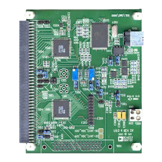
Page 35: Assembly-Primary Side
HSC-ADC-EVALA-SC/HSC-ADC-EVALA-DC ASSEMBLY—PRIMARY SIDE Figure 34. Assembly—Primary Side Rev. 0 | Page 35 of 44... -
Page 36: Assembly-Secondary Side
HSC-ADC-EVALA-SC/HSC-ADC-EVALA-DC ASSEMBLY—SECONDARY SIDE Figure 35. Assembly—Secondary Side Rev. 0 | Page 36 of 44... -
Page 37: Layer 1- Primary Side
HSC-ADC-EVALA-SC/HSC-ADC-EVALA-DC LAYER 1— PRIMARY SIDE Figure 36. Layer 1—Primary Side Rev. 0 | Page 37 of 44... -
Page 38: Layer 2-Ground Plane
HSC-ADC-EVALA-SC/HSC-ADC-EVALA-DC LAYER 2—GROUND PLANE Figure 37. Layer 2—Ground Plane Rev. 0 | Page 38 of 44... -
Page 39: Layer 3-Power Plane
HSC-ADC-EVALA-SC/HSC-ADC-EVALA-DC LAYER 3—POWER PLANE Figure 38. Layer 3—Power Plane Rev. 0 | Page 39 of 44... -
Page 40: Layer 4-Secondary Side
HSC-ADC-EVALA-SC/HSC-ADC-EVALA-DC LAYER 4—SECONDARY SIDE Figure 39. Layer 4—Secondary Side ESD CAUTION ESD (electrostatic discharge) sensitive device. Electrostatic charges as high as 4000 V readily accumulate on the human body and test equipment and can discharge without detection. Although this product features proprietary ESD protection circuitry, permanent damage may occur on devices subjected to high energy electrostatic discharges. -
Page 41: Bill Of Materials
HSC-ADC-EVALA-SC/HSC-ADC-EVALA-DC BILL OF MATERIALS Table 5. HSC-ADC-EVAL-SC/HSC-ADC-EVAL-DC Bill of Materials Quantity Reference Item Designation Description Package Value Manufacture C101–108, C201–208, C301–304, C306, C402–405, C503, Capacitor 0805 0.1 µF C506–517, C601 C305, C308, C310–311 Capacitor, 50 V, 20% 1206 0.1 µF... - Page 42 HSC-ADC-EVALA-SC/HSC-ADC-EVALA-DC Quantity Reference Item Designation Description Package Value Manufacture R504–507, R510–515, R520, Resistor, 1/8 W, 1% 1206 24.9 Ω R525–526 R508–509 Resistor, 1/10 W, 1% 0805 10 kΩ R516–517 Resistor, 1/8 W, 1% 1206 2 kΩ R521–522 Resistor, 1/10 W, 1% 0805 0 Ω...
-
Page 43: Appendix: Sampling And Fft Fundamentals
HSC-ADC-EVALA-SC/HSC-ADC-EVALA-DC APPENDIX: SAMPLING AND FFT FUNDAMENTALS COHERENT SAMPLING M = Sample Size (2 In a coherent system, the analog and clock sources must be n = Indexed Sample Number synchronized, and the analog and clock input frequencies must be selected such that given 2... -
Page 44: Ordering Guide
Required for Revision C of AD6644 and AD6645 evaluation boards. Revision D and greater are directly compatible with e HSC-ADC-EVALA-SC evaluation board © 2004 Analog Devices, Inc. All rights reserved. Trademarks and registered trademarks are the property of their respective owners.
Need help?
Do you have a question about the HSC-ADC-EVALA-SC and is the answer not in the manual?
Questions and answers