Table of Contents
Advertisement
Quick Links
Advertisement
Table of Contents

Related Manuals for Advantech PCM-3753I-AE


Summary of Contents for Advantech PCM-3753I-AE
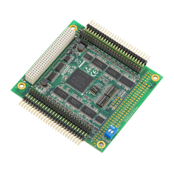
- Page 1 PCM-3753I 96-channel Digital I/O PCI-104 Module User Manual...
- Page 2 This documentation and the software included with this product are copyrighted 2008 by Advantech Co., Ltd. All rights are reserved. Advantech Co., Ltd. reserves the right to make improvements in the prod- ucts described in this manual at any time without notice.
- Page 3 Product Warranty (2 years) Advantech warrants to you, the original purchaser, that each of its prod- ucts will be free from defects in materials and workmanship for two years from the date of purchase. This warranty does not apply to any products which have been repaired or...
- Page 4 Technical Support and Assistance Step 1. Visit the Advantech web site at www.advantech.com/support where you can find the latest information about the product. Step 2. Contact your distributor, sales representative, or Advantech's customer service center for technical support if you need addi- tional assistance.
-
Page 5: Table Of Contents
Contents Chapter 1 General Information ........2 Introduction ............... 2 Features ................4 Applications ..............4 Specifications ..............5 Pin Assignments (CN5~CN8) ........... 6 Chapter 2 Installation ............8 Initial Inspection..............8 Unpacking ................. 8 Jumper Settings ..............9 Figure 2.1:Location of Connectors and Jumpers ... 9 Table 2.1:Summary of Jumper Settings ....... - Page 6 PCM-3753I User Manual...
- Page 7 General Information...
-
Page 8: Chapter 1 General Information
Chapter 1 General Information 1.1 Introduction The PCM-3753I is a 96-ch digital I/O PCI-104 module. The card emu- lates mode 0 of the 8255 PPI chip, but the buffered circuits offer a higher driving capability than the 8255. The 96 I/O lines are divided into twelve 8-bit I/O ports: A0, B0, C0, A1, B1, C1, A2, B2, C2, A3, B3 and C3. - Page 9 Interrupt Functions Ensure Faster System Response Two lines of each port C (i.e., ports C0, C1, C2 and C3) are connected to an interrupt circuit. The “Interrupt Control Register” of the PCM-3753I controls how these signals generate an interrupt. More than one interrupt request signals can be generated at the same time, and then the software can process these request signals by ISR.
-
Page 10: Features
1.2 Features • 96 TTL digital I/O lines • Emulates mode 0 of 8255 PPI • Buffered circuits for higher driving capacity than 8255 • Multiple-source interrupt handling • Output status read-back • “Pattern match” and “Change of state” interrupt functions for critical I/O monitoring •... -
Page 11: Specifications
1.4 Specifications I/O Channels 96 digital I/O lines Programming Mode 8255 PPI mode 0 Input Signal Logic level 0: 0.8 V max. Logic level 1: 2.0 V min. Output Signal Logic level 0: 0.44 V max. @ 24 mA (sink) Logic level 1: 3.76 V min. -
Page 12: Pin Assignments (Cn5~Cn8)
1.5 Pin Assignments (CN5~CN8) CN5: A0, B0, C0 CN6: A1, B1, C1 CN7: A2, B2, C2 CN8: A3, B3, C3 PCM-3753I User Manual... - Page 13 Installation...
-
Page 14: Chapter 2 Installation
Chapter 2 Installation 2.1 Initial Inspection Before starting to install the PCM-3753I, make sure there is no visible damage on the card. We carefully inspected the card both mechanically and electrically before shipment. It should be free of marks and in perfect order on receipt. As you unpack the PCM-3753I, check it for signs of shipping damage (damaged box, scratches, dents, etc.). -
Page 15: Jumper Settings
2.3 Jumper Settings We designed the PCM-3753I with ease-of-use in mind. It is a "plug and play" card, i.e. the system BIOS assigns the system resources such as base address and interrupt automatically. The following section describes how to configure the card. You may want to refer to the figure below for help in identifying card components. - Page 16 Using Jumpers to Set Ports as Output Ports By shorting the two pins of the jumpers JPA0, JPB0, JPC0L, JPC0H, JPA1, JPB1, JPC1L, JPC1H, JPA2, JPB2, JPC2L, JPC2H, JPA3, JPB3, JPC3L or JPC3H, a user sets the corresponding ports to be output ports. (JPA0 means jumper for port A0, JPB0 means jumper for port B0, etc.) Shorting the two pins of a port's jumper disables the port from being soft- ware configurable as an input port.
-
Page 17: Setting The Boardid Switch (Sw2)
2.4 Setting the BoardID Switch (SW2) You can use the BoardID command (0x20) to get the board’s unique iden- tifier. PCM-3753I has a built-in BoardID SMD switch (SW2), which is used to define each card's unique identifier. You can determine the identi- fier in the register as shown in Table 2.2. -
Page 18: Sw3 & Sw4 Settings
2.5 SW3 & SW4 Settings When set to “On (0)”, the Digital Port will be set to Output. When set to “Off (1)”, the Digital Port will be set by software. (Default) 2.6 Hardware Installation Turn the PC’s power off. Turn off the power of any peripheral devices such as printers and monitors. - Page 19 Operation...
-
Page 20: Chapter 3 Operation
Chapter 3 Operation 3.1 Overview This chapter describes the operating characteristics of the PCM-3753I. The driver software bundled with this card allows a user to access all of the card's functions without register level programming. Please see the User's Manual included on the driver CD-ROM for more information. For users who prefer to implement their own bit-level programming to drive the card's functions, information useful for making such a program is included in this chapter. -
Page 21: Input/Output Control
3.2.3 Input/Output Control A control word can be written to a port's configuration register (Base+3, 7, 11 and 15 respectively for ports 0, 1, 2 and 3 on the PCM-3753I, and Base+35, 39, 43 and 47 respectively for ports 0, 1, 2 and 3 on the PCM-3753IE) to set the port as an input or an output port, unless the ports are set as output ports via jumpers (refer to Section 2.3, Jumper Settings). -
Page 22: Dry Contact Support For Digital Input
If the jumper JP1 is enabled and the initial configuration is caused by a reset, all ports will return to the states they had just prior to the reset. The reset must be a "hot" reset (power not disconnected) for enabled JP1 to return ports to their prior values. -
Page 23: Interrupt Functions
3.3 Interrupt Functions 3.3.1 Introduction Two lines of each I/O port C, plus ports A0 and B0, are connected to the interrupt circuitry. The “Interrupt Control Register” of the PCM-3753I controls how the combination of these signals generates an interrupt. Six interrupt request signals can be generated at the same time, and then the software can service these six request signals by IRQ. - Page 24 Table 3.2: Interrupt Control Register Bitmap Base+16/48 Port 0 Bit # Abbreviation Base+17/49 Port 1 Bit # Abbreviation Base+18/50 Port 2 Bit # Abbreviation Base+19/51 Port 3 Bit # Abbreviation Mn0 and Mn1: “mode bits” of port Cn (n = 0 ~ 3) M1: pattern match port enable control bit of port A0 M2: change of state port enable control bit of port B0 En: triggering edge control bit (n = 0 ~ 3)
- Page 25 M01:M00 PC00 PC04 M11:M10 PC10 PC14 M21:M20 PC20 PC24 M31:M30 INT #A PC30 PC34 Pattern Match (PA0) Change of State (PB0) Figure 3.2: Interrupt Sources Chapter 3...
-
Page 26: Interrupt Source Control
3.3.4 Interrupt Source Control The “mode bits” in the interrupt control registers determine the allowable sources of signals generating an interrupt. For the PCM-3753I, bit 4 and bit 5 of Base+16 determines the interrupt source of port C0, bit 4 and bit 5 of Base+17 determines the interrupt source for port C1, and so forth. -
Page 27: Interrupt Triggering Edge Control
3.3.5 Interrupt Triggering Edge Control The interrupt can be triggered by a rising edge or a falling edge of the interrupt signal, selectable by the value written in the “triggering edge control” bit in the interrupt control register, as shown in following table. Table 3.4: Triggering Edge Control Bit Values En (n = 0 ~ 3) Triggering edge of interrupt signal... -
Page 28: Pattern Match Interrupt Function
3.3.7 Pattern Match Interrupt Function The PCM-3753I provides the pattern match interrupt function for port A0. It monitors the status of the enabled input channels, which are cho- sen in Base+24 (or Base+56 for the PCM-3753IE), and compares the received state values with the pre-set state values written in Base+20 (Base+52 for the PCM-3753IE). -
Page 29: Change Of State Interrupt Function
d) When the input signals at channels PA01, PA02 and PA07 are high and PA06 is low, an interrupt signal will be generated. This result is not affected by the states of channels PA00, PA03, PA04 and PA05. 3.3.8 Change of State Interrupt Function The PCM-3753I also provides the change of state interrupt function for port B0. - Page 30 PCM-3753I User Manual...
Need help?
Do you have a question about the PCM-3753I-AE and is the answer not in the manual?
Questions and answers