Table of Contents
Advertisement
Quick Links
Advertisement
Table of Contents

Related Manuals for Advantech PCI-1750SO


Summary of Contents for Advantech PCI-1750SO
- Page 1 User Manual PCI-1750/PCI-1750SO 32-ch Isolated Digital I/O PCI Card...
- Page 2 No part of this manual may be reproduced, copied, translated or transmitted in any form or by any means without the prior written permission of Advantech Co., Ltd. Information provided in this manual is intended to be accurate and reliable. How- ever, Advantech Co., Ltd.
- Page 3 This product has passed the CE test for environmental specifications when shielded cables are used for external wiring. We recommend the use of shielded cables. This kind of cable is available from Advantech. Please contact your local supplier for ordering information.
- Page 4 REPLACED. REPLACE ONLY WITH THE SAME OR EQUIVALENT TYPE RECOMMENDED BY THE MANUFACTURER, DISCARD USED BATTERIES ACCORDING TO THE MANUFACTURER'S INSTRUCTIONS. The sound pressure level at the operator's position according to IEC 704-1:1982 is no more than 70 dB (A). PCI-1750/PCI-1750SO User Manual...
- Page 5 Safety Precaution - Static Electricity DISCLAIMER: This set of instructions is given according to IEC 704-1. Advantech disclaims all responsibility for the accuracy of any statements contained herein.Safety Precaution - Static Electricity Follow these simple precautions to protect yourself from harm and the products from damage.
- Page 6 PCI-1750/PCI-1750SO User Manual...
-
Page 7: Table Of Contents
Interrupt function of the DIO signals ........... 14 3.2.3 Power On Configuration.............. 14 3.2.4 Isolated Inputs................15 Figure 3.1 PCI-1750 / PCI-1750SO isolated digital input connec- tion................15 3.2.5 Isolated Outputs................16 Figure 3.2 PCI-1750 isolated digital output connection (sink type) Figure 3.3 PCI-1750SO isolated digital output connection (source... - Page 8 MODE 5 – Hardware triggered strobe ........27 Counter operations ................. 27 A.3.1 Read/write operation..............27 A.3.2 Counter read-back command ............. 27 A.3.3 Counter latch operation .............. 27 Appendix B Register Format of PCI-1750/PCI- 1750SO29 Register Format of PCI-1750/PCI-1750SO..........30 PCI-1750/PCI-1750SO User Manual viii...
-
Page 9: Chapter 1 Overview
Chapter Overview... -
Page 10: Introduction
PC. A user can easily configure the interrupts through software. The PCI-1750/PCI-1750SO uses a PCI controller to interface the card to the PCI bus. The controller fully implements the PCI bus specification Rev 2.1. All bus relative configurations, such as base addresses and interrupt assignments, are automatically controlled by software. - Page 11 One 2-pin terminal block for extended ground Power consumption: 5 V @ 850 mA (Typical) 5 V @ 1.0 A (Max.) Operating temperature: 0 ~ 70ºC (32ºF ~ 158ºF) Storage temperature: -20 ~ 80ºC (-4ºF ~ 176ºF) Humidity: 5% ~ 95% non-condensing PCI-1750/PCI-1750SO User Manual...
- Page 12 PCI-1750/PCI-1750SO User Manual...
-
Page 13: Chapter 2 Installation
Chapter Installation... -
Page 14: Initial Inspection
Initial inspection Before starting to install the PCI-1750/PCI-1750SO, make sure there is no visible damage on the card. We carefully inspected the card both mechanically and electri- cally before shipment. It should be free of marks and in perfect order on receipt. -
Page 15: Location Of Connectors
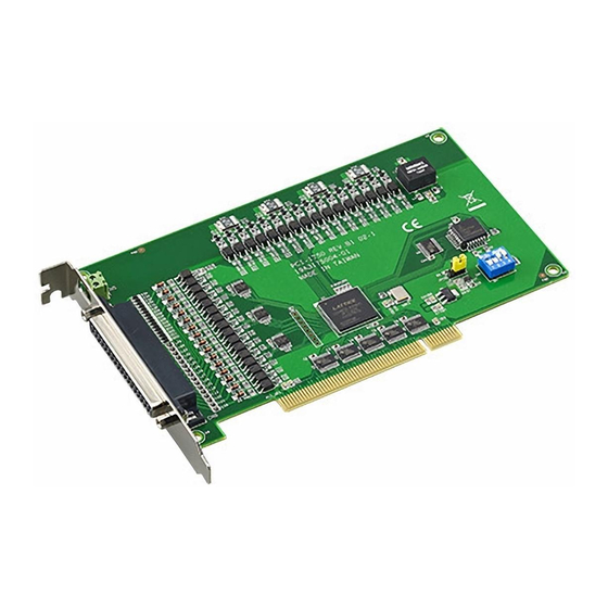
Location of Connectors Figure 2.1 shows the names and locations of connectors on the board. The PCI-1750/PCI-1750SO is a plug and play device. The PCI BIOS assigns the sys- tem resources automatically at system start-up. All functions can be set by software. - Page 16 Board ID (SW1) The PCI-1750/PCI-1750SO has a built-in DIP switch (SW1), which is used to define each cards board ID. When there are multiple cards on the same chassis, this board ID switch is useful for identifying each cards device number.
-
Page 17: Pci-1750/Pci-1750So Block Diagram
PCI-1750/PCI-1750SO Block Diagram Figure 2.2 Block Diagram PCI-1750/PCI-1750SO User Manual... -
Page 18: Connector Pin Assignments
Isolated ground INT<0,1> IGND Input Interrupt trigger sources (shared with IDI 0, IDI 8) INT<0,1>_G IGND Gate for Interrupt pins (shared with IDI 4, IDI 12) Counter2 IGND Input Input pin of isolated counter (shared with IDI 15) PCI-1750/PCI-1750SO User Manual... - Page 19 Warning! Be careful when wiring digital input lines. Never apply a negative voltage to the isolated input pins, as this may damage the PCI-1750/PCI- 1750SO. PCI-1750/PCI-1750SO User Manual...
-
Page 20: Installation Instructions
Installation Instructions The PCI-1750/PCI-1750SO can be installed in any PCI slot in the computer.How ever, refer to the computer user's manual to avoid any mistakes and danger before you follow the installation procedure below: Turn off your computer and any accessories connected to the computer. -
Page 21: Chapter 3 Operation
Chapter Operation... -
Page 22: Operation
Isolated Digital I/O Ports 3.2.1 Introduction The PCI-1750/PCI-1750SO has 16 isolated digital input channels designated IDI 0 ~ IDI 15, and 16 isolated digital output channels designated IDO 0 ~ IDO 15. Data can be read from or written to the card's channels. -
Page 23: Isolated Inputs
(>5 K ). It is advisable to Ω connect a parallel 5 K , 0.5 W resistor to avoid a voltage rise inside the voltage Ω source. Figure 3.1 PCI-1750 / PCI-1750SO isolated digital input connection PCI-1750/PCI-1750SO User Manual... -
Page 24: Isolated Outputs
Figure 3.2 shows how to connect an external output load to the card's isolated out- puts. Figure 3.2 PCI-1750 isolated digital output connection (sink type) Figure 3.3 PCI-1750SO isolated digital output connection (source type) PCI-1750/PCI-1750SO User Manual... -
Page 25: Timer And Counter
IDI 15). The block diagram of the timer/counter system of PCI-1750/ PCI-1750SO is shown in Figure 3.3. Timers 0 and 1 are usually set in mode 3 (square wave generator) to generate periodic watchdog interrupts. Counter 2 can be... -
Page 26: One Shot And Interrupt
The One-Shot, which is based on counting function to achieve and can be triggered by external signal level change. For example as figure 3.5, the number of counting is set to 3 so that an interrupt will be generated after 3 cycles of external clock signal is received. PCI-1750/PCI-1750SO User Manual... -
Page 27: Interrupt Function
Four input channels (IDI 0, IDI 4, IDI 8 and IDI 12) and the output of Timer 1 and Counter 2 are connected to the interrupt circuitry. The “Interrupt Control Register” of the PCI-1750/PCI-1750SO controls how the combination of the six signals generates an interrupt. Two interrupt request signals, designated “interrupt group 0" and “inter- rupt group 1", can be generated at the same time, and then the software can service... -
Page 28: Interrupt Source Control
“triggering edge control” bit in the interrupt control register, as shown in Table 3.3. Table 3.3: Triggering edge control bit values E0 or E1 Triggering edge of interrupt signal Rising edge trigger Falling edge trigger PCI-1750/PCI-1750SO User Manual... -
Page 29: Interrupt Flag Bit
This bit must be cleared in the ISR to service the next incom- ing interrupt. Table 3.4: Interrupt flag bit values F0 & F1 Interrupt status Read Interrupt No Interrupt Write Clear Interrupt Don’t Care PCI-1750/PCI-1750SO User Manual... - Page 30 PCI-1750/PCI-1750SO User Manual...
-
Page 31: Appendix A Function Of 8254 Counter Chip
Appendix Function of 8254 Counter Chip... -
Page 32: The Intel 8254
The 8254 has a maximum input clock frequency of 10 MHz. The PCI-1750/PCI- 1750SO provides 10 MHz input frequencies to the counter chip from an on-board crystal oscillator. On the PCI-1750/PCI-1750SO, the 8254 chip's Timer 0 and Timer 1 are cascaded to be a 32-bit programmable timer. A.1.1... - Page 33 The data format of the counter read/write register then becomes: BASE+24/25/26(Dec) Status read-back mode Value OUT Current state of counter output Null count is 1 when the last count written to the counter register has been loaded into the counting element PCI-1750/PCI-1750SO User Manual...
-
Page 34: Counter Operating Modes
(following the reload) decrements the counter by 3. Subsequent clock pulses decrement the count by two until time out, then the whole process is repeated. In this way, if the count is odd, the output will be high for (N+1)/2 counts and low for (N-1)/2 counts. PCI-1750/PCI-1750SO User Manual... -
Page 35: Mode 4 - Software Triggered Strobe
Set bits SC1 and SC0 to 1 and CNT = 0. The second method has the advan- tage of operating several counters at the same time. A subsequent read operation on the selected counter will retrieve the latched value. PCI-1750/PCI-1750SO User Manual... - Page 36 PCI-1750/PCI-1750SO User Manual...
-
Page 37: Register Format Of Pci-1750/Pci
Appendix Register Format of PCI-1750/PCI-1750SO... -
Page 38: Register Format Of Pci-1750/Pci-1750So
Register Format of PCI-1750/PCI-1750SO Function Base Address + (Decimal) Read Write IDI [7:0] IDO [7:0] IDI [15:8] IDO [15:8] IDO [7:0] Read back Reserved IDO [15:8] Read back Reserved BOID [3:0] Reserved 5~23 Reserved Reserved 8254 Counter 0 8254 Counter 0... - Page 39 PCI-1750/PCI-1750SO User Manual...
- Page 40 No part of this publication may be reproduced in any form or by any means, electronic, photocopying, recording or otherwise, without prior written permis- sion of the publisher. All brand and product names are trademarks or registered trademarks of their respective companies. © Advantech Co., Ltd. 2016...
Need help?
Do you have a question about the PCI-1750SO and is the answer not in the manual?
Questions and answers