
Related Manuals for Quanmax KEEX-6150 Series


Summary of Contents for Quanmax KEEX-6150 Series
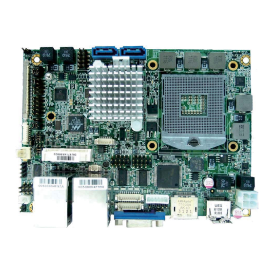
- Page 1 KEEX-6100 Series Industrial ECX Embedded SBC with 2nd generation Intel® core i3/i5/i7 processor User’s Guide KEEX-6100 Series User’s Manual...
- Page 2 © 2011 Quanmax Inc. All rights reserved. The information in this user’s guide is provided for reference only. Quanmax does not assume any liability arising out of the application or use of the information or products described herein. This user’s guide may contain or reference information and products protected by copyrights or patents and does not convey any license under the patent rights of Quanmax, nor the rights of others.
-
Page 3: Table Of Contents
Content Content Content........................3 Figures ........................5 Tables......................... 6 Safety Instructions...................... 8 Before You Begin..................8 When Working Inside a Computer............... 8 Preventing Electrostatic Discharge.............. 9 Preface........................11 How to Use This Guide................11 Unpacking....................11 Regulatory Compliance Statements ............11 Warranty Policy .................. - Page 4 Content Chapter 5 Driver Installation .................. 55 Appendix A DIO (Digital I/O) Sample Code............56 Appendix B WatchDog Timer Sample Code............. 58 KEEX-6100 Series User’s Manual...
-
Page 5: Figures
Figures Figures Figure 1 Block Diagram ................19 Figure 2 Mechanical Dimensions ............... 21 Figure 3 Jumper Connector ............... 22 Figure 4 Jumper and Connector Locations ..........23 Figure 5 Rear Panel IO ................26 Figure 6 Align the SO-DIMM Memory Module with the onboard socket..37 Figure 7 Press down on the SO-DIMM Memory Module to lock it in place 38 KEEX-6100 Series User’s Manual... -
Page 6: Tables
Tables Tables Table 1 KEEX-6100 Series Specification ........... 18 Table 2 Jumper List..................24 Table 3 JP1 ME F/W Selection..............24 Table 4 JP2 Panel & Backlight Power Selection for LVDS2 ....... 24 Table 5 JP3 Panel Backlight Power Selection for LVDS1......25 Table 6 JP4 Backlight Power Enable Selection for LVDS1 ...... - Page 7 Tables Table 35 DIMM1 DDR3 Memory SO-DIMM Socket ........33 Table 36 FAN1 CPU FAN Wafer..............33 Table 37 FP1 Front Panel 1 Pin Header ............ 33 Table 38 FP2 Front Panel 2 Pin Header ............ 33 Table 39 IR1 IrDA Pin Header ..............33 Table 40 LVDS1 Primary 24-bit, 2-channel LVDS Panel Connector...
-
Page 8: Safety Instructions
Use extreme caution when installing or removing components. Refer to the installation instructions in this user’s guide for precautions and procedures. If you have any questions, please contact Quanmax Post-Sales Technical Support. WARNING High voltages are present inside the chassis when the unit’s power cord is... -
Page 9: Preventing Electrostatic Discharge
Static electricity can harm system boards. Perform service at an ESD workstation and follow proper ESD procedure to reduce the risk of damage to components. Quanmax strongly encourages you to follow proper ESD procedure, which can include wrist straps and smocks, when servicing equipment. - Page 10 Safety Instructions When transporting a sensitive component, first place it in an antistatic container or packaging. Handle all sensitive components at an ESD workstation. If possible, use antistatic floor pads and workbench pads. Handle components and boards with care. Don’t touch the components or contacts on a board.
-
Page 11: Preface
Remove all items from the box. If any items listed on the purchase order are missing, notify Quanmax customer service immediately. Inspect the product for damage. If there is damage, notify Quanmax customer service immediately. Refer to “Warranty Policy” for the return procedure. -
Page 12: Warranty Policy
Quanmax or its authorized agent; or if the failure is caused by accident, acts of God, or other causes beyond the control of Quanmax or the manufacturer. Neglect, misuse, and abuse shall include any installation, operation, or maintenance of the product other than in accordance with the user’s guide. -
Page 13: Maintaining Your Computer
Quanmax. Limitation of Liability In no event shall Quanmax be liable for any defect in hardware, software, loss, or inadequacy of data of any kind, or for any direct, indirect, incidental, or consequential damages in connection with or arising out of the performance or use of any product furnished hereunder. - Page 14 Preface properties as electrical resistance and thermal conductivity. Extreme moisture buildup inside the system can result in electrical shorts, which can cause serious damage to the system. Buildings in which climate is controlled usually maintain an acceptable level of humidity for system equipment. However, if a system is located in an unusually humid location, a dehumidifier can be used to maintain the humidity within an acceptable range.
- Page 15 Preface Uninterruptible Power Supply Uninterruptible power supply (UPS) systems offer the most complete protection against variations on power because they use battery power to keep the server running when AC power is lost. The battery is charged by the AC power while it is available, so when AC power is lost, the battery can provide power to the system for a limited amount of time, depending on the UPS system.
-
Page 16: Chapter 1 Introduction
Chapter 1 Chapter 1 Introduction Overview The KEEX-6100 Series is an ECX Form Factor embedded single board computer (SBC) that equips the latest 2 generation Intel® Core™ i3/i5/i7 processors with the high integration of the Intel® QM67/ HM65 chipset. Featured are DDR3 1066/1333 SO-DIMM up to 8GB, 2x 24-bit LVDS, HDMI, DP, VGA, 2x Gigabit Ethernet, 2x SATA, mini PCIe slot, 8x USB 2.0, 2x COM ports with Power Selection, HD audio and CompactFlash. -
Page 17: Product Specifications
Chapter 1 Product Specifications KEEX-6100 Series Model Name ECX (146mm x 105mm) Form Factor Generation Intel core i3/i5/i7 Processors with rPGA988B package Processor 1x SO-DIMM, dual channel DDR3, non-ECC supported, up to 8GB Memory ® KEEX-6100---Intel QM67 Express Chipset Chipset ®... -
Page 18: Table 1 Keex-6100 Series Specification
Chapter 1 1x 1x6-pin pitch 2.00 mm wafer connector for PS/2 keyboard and mouse. 1x 1x5-pin pitch 2.54mm header for IrDA supported. 1x 1x3-pin fan connector onboard with smart fan supported. 1x 2x 5-pin pitch 2.54 mm header onboard for 8-bit DIO. 4-bit input and 4-bit output. -
Page 19: System Block Diagram
Chapter 1 System Block Diagram Figure 1 Block Diagram KEEX-6100 Series User’s Manual... -
Page 20: Mechanical Dimensions
Chapter 1 Mechanical Dimensions KEEX-6100 Series User’s Manual... -
Page 21: Figure 2 Mechanical Dimensions
Chapter 1 Figure 2 Mechanical Dimensions KEEX-6100 Series User’s Manual... -
Page 22: Chapter 2 Hardware Settings
Chapter 2 Chapter 2 Hardware Settings Overview This chapter provides the definitions and locations of jumpers, headers, and connectors. Jumpers The product has several jumpers which must be properly configured to ensure correct operation. Figure 3 Jumper Connector For a three-pin jumper (see Figure 3), the jumper setting is designated “1-2” when the jumper connects pins 1 and 2. -
Page 23: Jumper Settings And Pin Definitions
Chapter 2 Jumper Settings and Pin Definitions For jumper and connector locations, please refer to the diagrams below. Figure 4 Jumper and Connector Locations KEEX-6100 Series User’s Manual... -
Page 24: Jumper Settings
Chapter 2 Jumper Settings To ensure correct system configuration, the following section describes how to set the jumpers to enable/disable or change functions. For jumper descriptions, please refer to the table below Table 2 Jumper List Label Function ME F/W Selection Panel &... -
Page 25: Table 5 Jp3 Panel Backlight Power Selection For Lvds1
Chapter 2 Table 5 JP3 Panel Backlight Power Selection for LVDS1 Jumper Setting Status Backlight Power = +12V Backlight Power = +5V Panel Power = +3.3V Panel Power = +5V Pitch:2.54mm [YIMTEX 3362*03SAGR] Table 6 JP4 Backlight Power Enable Selection for LVDS1 Jumper Setting Status... -
Page 26: Rear Panel Pin Assignments
Chapter 2 Rear Panel Pin Assignments Figure 5 Rear Panel IO Table 11 Rear Panel Connector List Label Function LAN1 & USB2.0 Port 0,1 Connector CN10 LAN2 & USB2.0 Port 8,9 Connector Display Port Connector HDMI1 HDMI Connector VGA1 DB-15 VGA Connector Table 12 CN9 LAN1 &... -
Page 27: Table 14 Dp1 Display Port Connector
Chapter 2 Table 14 DP1 Display Port Connector Signal Signal TX0+ TX3- TX0- TX1+ AUX+ TX1- TX2+ AUX- TX2- TX3+ [WIN WIN WDPE-20F3L1BU3] Table 15 HDMI1 HDMI Connector Signal TMDS Data2+ Ground TMDS Data2– TMDS Data1+ Ground TMDS Data1– TMDS Data0+ Ground TMDS Data0–... -
Page 28: Main Board Pin Assignments
Chapter 2 Main Board Pin Assignments Table 17 Internal Connector List Label Function ATX1 +12V Power Input Connector BAT1 CR2032 Battery Power Input Wafer Onboard Buzzer CFD1 CF Type II Connector COM1 RS-232/422/485 Port 1 Wafer COM2 RS-232 Port 2 Wafer Digital Input / Output Pin Header SATA HDD Power Output Wafer Backlight Power Output Wafer for LVDS1... -
Page 29: Table 20 Cfd1 Cf Type Ii Connector
Chapter 2 Table 20 CFD1 CF Type II Connector Signal Name Signal Name IDE Data 3 IDE Data 11 IDE Data 4 IDE Data 12 IDE Data 5 IDE Data 13 IDE Data 6 IDE Data 14 IDE Data 7 IDE Data 15 IDE Chip select 1# 7 IDE Chip select 3#... -
Page 30: Table 21 Com1 Rs-232/422/485 Port 1 Wafer
Chapter 2 Table 21 COM1 RS-232/422/485 Port 1 Wafer Half Duplex Full Duplex RS-232 RS-422 RS-485 RS-485 DATA- DATA+ Pitch:1.25mm [Pinrex 712-73-10TWB0] Table 22 COM2 RS-232 Port 2 Wafer Signal Name Pitch:1.25mm [Pinrex 712-73-10TWB0] Table 23 CN1 Digital Input / Output Pin Header Signal Signal Digital Output 0... -
Page 31: Table 25 Cn3 Backlight Power Output Wafer For Lvds1
Chapter 2 Table 25 CN3 Backlight Power Output Wafer for LVDS1 Signal Name BL_ADJ_PWM * BL_ADJ_VOL * +5V / +12V ** +5V / +12V ** BL_EN*** Pitch:1.25mm [YIMTEX 501MW1X07MTR-1R] * BL_ADJ can be setting in BIOS setup. ** Backlight Power can be selected by JP3. *** BL_EN can be selected by JP4. -
Page 32: Table 29 Cn7 S/Pdif Pin Header
Chapter 2 Table 29 CN7 S/PDIF Pin Header Signal Name S/PDIF Input S/PDIF Output Pitch:2.54mm [YIMTEX 3321*04SAGR(6T)] Table 30 CN8 Audio Pin Header Signal Name Signal Name MIC_IN_L MIC_IN_R MIC_IN_JD LINE_IN_L LINE_IN_R LINE_IN_JD LINE_OUT_L LINE_OUT_R LINE_OUT_JD Pitch:2.54mm [PINREX 212-92-06GB01] Table 31 CN12 Left Channel 2W Audio AMP Output Wafer Signal Name Speaker+ Speaker-... -
Page 33: Table 34 Cn20 Keyboard & Mouse Wafer
Chapter 2 Table 34 CN20 Keyboard & Mouse Wafer Signal Name MSCLK MSDAT* KBDAT KBCLK Pitch:2.0mm [YIMTEX 503PW1*06STR] Table 35 DIMM1 DDR3 Memory SO-DIMM Socket Height: 7.0mm [LINKTEK DDRRK-20401-TP7B] Table 36 FAN1 CPU FAN Wafer Signal +12V* FAN_RPM PWM Fan control supported. Table 37 FP1 Front Panel 1 Pin Header Signal Signal... -
Page 34: Table 40 Lvds1 Primary 24-Bit, 2-Channel Lvds Panel Connector
Chapter 2 Table 40 LVDS1 Primary 24-bit, 2-channel LVDS Panel Connector Signal Name Signal Name LVDS_A0- LVDS_B1+ LVDS_A0+ LVDS_A1- LVDS_B2- LVDS_A1+ LVDS_B2+ LVDS_A2- LVDSBCLK- LVDS_A2+ LVDS_BCLK+ LVDS_B3-/NC LVDS_ACLK- LVDS_B3+/NC LVDS_ACLK+ LVDS_A3-/NC DDC_DATA LVDS_A3+/NC VDDEN LVDS_B0- DDC_CLK LVDS_B0+ +3.3V / +5V * +3.3V / +5V * LVDS_B1- +3.3V / +5V *... -
Page 35: Table 42 Mpcie1 Mini-Pcie Express V 1.2 Socket
Chapter 2 Table 42 MPCIE1 Mini-PCIE Express v 1.2 Socket Signal Signal WAKE# +3.3VSB Reserved Ground Reserved +1.5V CLKREQ# UIM_PWR* Ground UIM_DATA* REFCLK- UIM_CLK* REFCLK+ UIM_RESET* Ground UIM_VPP* Reserved Ground Reserved W_Disable# Ground PERST# PERn0 +3.3VSB PERp0 Ground Ground +1.5V Ground SMB_CLK PETn0... -
Page 36: Table 43 Sata1 Serial Ata Port 0 Connector
Chapter 2 Table 43 SATA1 Serial ATA Port 0 Connector Signal Name [FOXCONN LD1807V-S52U] Table 44 SATA2 Serial ATA Port 1 Connector Signal Name [FOXCONN LD1807V-S52U] KEEX-6100 Series User’s Manual... -
Page 37: Chapter 3 System Installation
Chapter 3 Chapter 3 System Installation Expansion Interfaces 1x full size mini-PCIe slot supported 1x connector onboard for SIM card signals supported NOTE When adding or removing expansion cards, make sure that you unplug the power supply first. Meanwhile, read the documentation for the expansion card to configure any necessary hardware or software settings for the expansion card, such as jumpers, switches or BIOS configuration. -
Page 38: Figure 7 Press Down On The So-Dimm Memory Module To Lock It In Place
Chapter 3 Fully insert the module into the socket until a “click” is heard. Press down on the SO-DIMM so that the tabs of the socket lock on both sides of the module Figure 7 Press down on the SO-DIMM Memory Module to lock it in place Removing a DIMM: To remove the SO-DIMM, use your fingers or a small screwdriver to carefully push away the tabs that secure either side of the SO-DIMM. -
Page 39: Chapter 4 Ami Bios Setup
This chapter provides a description of the AMI BIOS. The BIOS setup menus and available selections may vary from those of your product. For specific information on the BIOS for your product, please contact Quanmax. NOTE: The BIOS menus and selections for your product may vary from those in this chapter. -
Page 40: Main Menu
Chapter 4 Main Menu The BIOS Setup is accessed by pressing the DEL key after the Power-On Self-Test (POST) memory test begins and before the operating system boot begins. Once you enter the BIOS Setup Utility, the Main Menu will appear on the screen. The Main Menu provides System Overview information and allows you to set the System Time and Date. -
Page 41: Advanced Menu
Chapter 4 Advanced Menu Table 46 Advanced Menu BIOS SETUP UTILITY M a i n A d v a n c e d B o o t S e c u r i t y S e r v e r M g m t S a v e &... -
Page 42: Table 47 Advanced Menu - Display Configuration
Chapter 4 Table 47 Advanced Menu – Display Configuration BIOS SETUP UTILITY M a i n A d v a n c e d B o o t S e c u r i t y S e r v e r M g m t S a v e &... -
Page 43: Table 48 Advanced Menu - Super Io Configuration
Chapter 4 LVDS2 Panel Type Options: 640x480 18Bit 1CH, 800x480 18Bit 1CH, 800x600 18Bit 1CH, 1024x768 18Bit 1CH, 1440x900 18Bit 2CH, 1600x900 18Bit 2CH, 800x480 24Bit 1CH, 800x600 24Bit 1CH, 1024x768 24Bit 1CH, 1280x1024 24Bit 2CH, 1366x768 24Bit 1CH, 1366x768 24Bit 2CH, 1440x900 24Bit 2CH, 1600x1200 24Bit 2CH, 1920x1080 24Bit 2CH, 1920x1200 24Bit 2CH LVDS1 Backlight Control –... -
Page 44: Table 49 Advanced Menu - Super Io Configuration - Serial Port
Chapter 4 Table 49 Advanced Menu – Super IO Configuration – Serial Port 1 Configuration BIOS SETUP UTILITY M a i n A d v a n c e d B o o t S e c u r i t y S a v e &... -
Page 45: Table 51 Advanced Menu -Power Management Configuration
Chapter 4 Change Settings Options: Auto, IO=2F8h; IRQ=3; IO=3F8h; IRQ=3, 4, 5, 6, 7, 9, 10, 11, 12; IO=2F8h; IRQ=3, 4, 5, 6, 7, 9, 10, 11, 12; IO=3E8h; IRQ=3, 4, 5, 6, 7, 9, 10, 11, 12; IO=2E8h; IRQ=3, 4, 5, 6, 7, 9, 10, 11, 12; Device Mode Options: Standard Serial Port Mode, IrDA function, active pulse is 1.6us, IrDA function, active pulse is 3/16 bit time. -
Page 46: Table 52 Advanced Menu -Cpu Advanced Configuration
Chapter 4 Options: Disabled, Enabled Table 52 Advanced Menu –CPU Advanced Configuration BIOS SETUP UTILITY M a i n A d v a n c e d B o o t S e c u r i t y S a v e &... -
Page 47: Table 53 Advanced Menu -Trusted Computing
Chapter 4 Table 53 Advanced Menu –Trusted Computing BIOS SETUP UTILITY M a i n A d v a n c e d B o o t S e c u r i t y S a v e & E x i t TPM Configuration Enable/Disable TPM support. -
Page 48: Table 55 Advanced Menu -Intel Txt(Lt) Configuration
Chapter 4 Table 55 Advanced Menu –Intel TXT(LT) Configuration BIOS SETUP UTILITY M a i n A d v a n c e d B o o t S e c u r i t y S a v e &... - Page 49 Chapter 4 MEBx Selection Screen Options: Disabled, Enabled Verbose MEBx Output Options: Disabled, Enabled Hide Un-Configure ME Confirmation Options: Disabled, Enabled MEBx Debug Message Output Un-Configure ME Options: Disabled, Enabled Intel AMT Password Write Enabled Options: Disabled, Enabled AMT Wait Timer Options: 0 only Options: Disabled, Enabled Activate Remote Assistance Process...
-
Page 50: Table 57 Advanced Menu -Usb Configuration
Chapter 4 Table 57 Advanced Menu –USB Configuration BIOS SETUP UTILITY M a i n A d v a n c e d B o o t S e c u r i t y S a v e & E x i t USB Configuration Enables Legacy USB support. -
Page 51: Table 58 Advanced Menu -H/W Monitor
Chapter 4 Table 58 Advanced Menu –H/W Monitor BIOS SETUP UTILITY M a i n A d v a n c e d B o o t S e c u r i t y S a v e & E x i t PC Health Status CPU Warning Temperature... -
Page 52: Boot Menu
Chapter 4 Boot Menu Table 59 Boot Menu BIOS SETUP UTILITY M a i n A d v a n c e d B o o t S e c u r i t y S a v e & E x i t Boot Configuration Enables or Disables Quiet Boot Full Screen LOGO Display... -
Page 53: Security Menu
Chapter 4 Security Menu Table 60 Security Menu BIOS SETUP UTILITY M a i n A d v a n c e d B o o t S e c u r i t y S a v e & E x i t Password Description Set Setup Administrator Password... - Page 54 Chapter 4 Save Changes and Exit Exit system setup after saving the changes. Once you are finished making your selections, choose this option from the Exit menu to ensure the values you selected are saved to the CMOS RAM. The CMOS RAM is sustained by an onboard backup battery and stays on even when the PC is turned off.
- Page 55 After you have finished assembling your system and connected the appropriate power source, power it up using the power supply and install the desired operating system. You can download the drivers for the KEEX-6100 Series from the Quanmax website www.quanmax.com and install as instructed there. For other operating systems, please contact Quanmax.
- Page 56 Appendix A Appendix A DIO (Digital I/O) Sample Code //*************************************************************** //KEEX-6100 DOS DIO sample program //Please compile with Turbo C 3.0 to utilized the program //0:Low 1:High //DI_1: IOport 0x50C bit2 DO_1: IOport 0x539 bit4 //DI_2: IOport 0x50C bit3 DO_2: IOport 0x539 bit5 //DI_3: IOport 0x50C bit4 DO_3: IOport 0x539 bit6 //DI_4: IOport 0x50C bit5 DO_4: IOport 0x53B bit0 //***************************************************************...
- Page 57 Appendix A //DO_2 is bit 5 //DO_3 is bit 6 outp(0x539,RetVal); RetVal=inp(0x53B);//IO Port: 0x53B RetVal=(RetVal|0x01);//DO_4 is bit 0 outp(0x53B,RetVal); system("pause"); //Reading DI_1~4 RetVal=inp(0x50C);//IO Port: 0x50C RetVal=(RetVal&0x3C);//DI_1 is bit 2 //DI_2 is bit 3 //DI_3 is bit 4 //DI_4 is bit 5 printf("DI_= %d\n",RetVal);...
- Page 58 Appendix B Appendix B WatchDog Timer Sample Code //============================================ //KEEX-6100 DOS Watchdog sample program //Please compile with Turbo C 3.0 to utilized the program //============================================ #include<stdio.h> int main() int value; //Initialized the WDT program outp(0x2E,0x87); outp(0x2E,0x87); //Setting Logical Device Number to 0x07 outp(0x2E,0x07);...
- Page 59 Appendix B outp(0x2E,0xF0); outp(0x2F,0x81);//bit7 WDTRST# output is enabled return 0; KEEX-6100 Series User’s Manual...
Need help?
Do you have a question about the KEEX-6150 Series and is the answer not in the manual?
Questions and answers