
Related Manuals for Quanmax ECX-SLU0 Series


Summary of Contents for Quanmax ECX-SLU0 Series
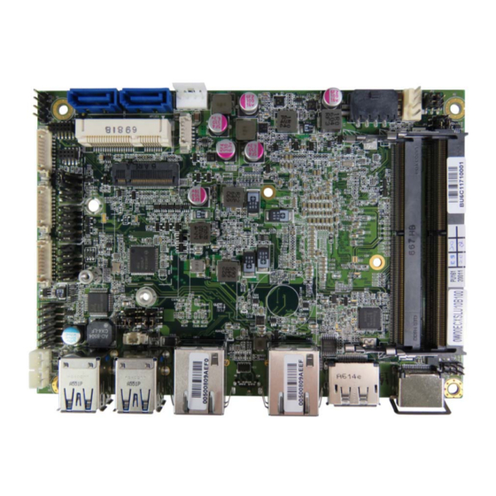
- Page 1 ECX-SLU0 / KLU0 Series 3.5" ECX Single Board Computer ® with Intel Skylake / Kaby Lake U-Series Processors User’s Guide ECX-SLU0 / KLU0 Series Use r’s Manual...
- Page 2 © 2017 Quanmax Inc. All rights reserved. The information in this user’s guide is provided for reference only. Quanmax does not assume any liability arising out of the application or use of the information or products described herein. This user’s guide may contain or reference information and products protected by copyrights or patents and does not convey any license under the patent rights of Quanmax, nor the rights of others.
-
Page 3: Table Of Contents
Content Content Content............................3 Figures ............................5 Tables ............................6 Safety Instructions........................8 Before You Begin ....................8 When Working Inside a Computer ...............8 Preventing Electrostatic Discharge ..............9 Preface ............................ 11 How to Use This Guide ..................11 Unpacking ......................11 ... - Page 4 Content Chapter 5 Driver Installation .....................54 Appendix A DIO (Digital I/O) Sample Code ..............55 Appendix B WatchDog Timer Sample Code ..............59 ECX-SLU0 / KLU0 Series Use r’s Manual...
-
Page 5: Figures
Figures Figures Figure 1 Block Diagram ..................18 Figure 2 Mechanical Dimensions................19 Figure 3 Jumper Connector .................20 Figure 4 Jumper and Connector Locations ............21 Figure 5 Rear Panel IO..................32 Figure 6 Align the SO-DIMM Memory Module with the onb oard socket ..35 Figure 7 Press down on the SO-DIMM Memory Module to lock it in place .36 ECX-SLU0 / KLU0 Series Use r’s Manual... -
Page 6: Tables
Tables Tables Table 1 ECX-BW00 Specification................17 Table 2 Jumper List ....................22 Table 3 JP1 MPCIE1 Activity LED Pin Header ..........22 Table 4 JP2 Panel & Backlight Power Selection for LVDS1......22 Table 5 JP3 NGFF M.2 Acti vity LED Pin Header ..........22 Table 6 JP4 Backlight Power Enable Selection for LVDS1......23 Table 7 JP6 AT / ATX Power Mode and NGFF mSATA/mPCIe Selection ..23 Table 8 JP7 SIM Card and MPCIE mSATA/mPCIe Selection, USB Power... - Page 7 Tables Table 34 CN12 GbE LAN1 RJ-45 Connector............33 Table 35 CN11 GbE LAN2 RJ-45 Connector ............33 Table 36 CN13 USB3.0/3.1 Port-1,3.1-1b Type-A Connector ......34 Table 37 CN14 USB3.0 Port-3,4 Type-A Connector ........34 Table 38 ECX-SLU0 / KLU0 Series BIOS Main Menu........38 Table 39 Ad vanced Menu..................39 Table 40 Ad vanced Menu –...
-
Page 8: Safety Instructions
Use extreme caution when installing or removing components. Refer to the installation instructions in this user’s guide for precautions and procedures. If you have any questions, please contact Quanmax Post-Sales Technical Support. WARNING High voltages are present inside the chassis when the unit’s power cord is plugged into an electrical outlet. -
Page 9: Preventing Electrostatic Discharge
Static electricity can harm system boards. Perform service at an ESD workstation and follow proper ESD procedure to reduce the risk of damage to components. Quanmax strongly encourages you to follow proper ESD procedure, which can include wrist straps and smocks, when servicing equipment. - Page 10 Safety Instructions When transporting a sensitive component, first place it in an antistatic container or packaging. Handle all sensitive components at an ESD workstation. If possible, use antistatic floor pads and workbench pads. Handle components and boards with care. Don’t touch the components or contacts on a board.
-
Page 11: Preface
Remove all items from the box. If any items listed on the purchase order are missing, notify Quanmax customer service immediately. Inspect the product for damage. If there is damage, notify Quanmax customer service immediately. Refer to “Warranty Policy” for the return procedure. -
Page 12: Warranty Policy
Quanmax or its authorized agent; or if the failure is caused by accident, acts of God, or other causes beyond the control of Quanmax or the manufacturer. Neglect, misuse, and abuse shall include any installation, operation, or maintenance of the product other than in accordance with the user’s guide. -
Page 13: Maintaining Your Computer
Quanmax. Limitation of Liability In no event shall Quanmax be liable for any defect in hardware, software, loss, or inadequacy of data of any kind, or for any direct, indirect, incidental, or consequential damages in connection with or arising out of the performance or use of any product furnished hereunder. - Page 14 Preface properties as electrical resistance and thermal conductivity. Extreme moisture buildup inside the system can result in electrical shorts, which can cause serious damage to the system. Buildings in which climate is controlled usually maintain an acceptable level of humidity for system equipment. However, if a system is located in an unusually humid location, a dehumidifier can be used to maintain the humidity within an acceptable range.
- Page 15 Preface Uninterruptible Power Supply Uninterruptible power supply (UPS) systems offer the most complete protection against variations on power because they use battery power to keep the server running when AC power is lost. The battery is charged by the AC power while it is available, so when AC power is lost, the battery can provide power to the system for a limited amount of time, depending on the UPS system.
-
Page 16: Chapter 1 Introduction
Chapter 1 Chapter 1 Introduction Overview ECX-SLU0 / KLU0 Series is a 3.5" ECX Single Board Computer based on Intel Skylake / Kaby Lake U-Series Processors, providing an upgraded option for high performance platform finders. It has 4 shinning features to make it distinguish from other counterparts, including (1) 2x SATA3.0 for doubling read and write speeds;... -
Page 17: Product Specifications
Chapter 1 Product Specifications Model Name ECX‐SLU0 / KLU0 Series For m Factor ECX, 146x105mm CPU Support Intel® Skylake / Kaby Lake U‐Series Processor (TDP=15W) Memory 2x DDR4 2133 SO‐DIMM Socket 1x LVDS (24‐bit, 2‐ch) 1x HDMI2.0 (on rear) Displays 1x DP (on rear) Triple Display Support Audio Chipset Realtek ALC662 2x Speaker‐out (3W) 1x Line‐in (by header) Audio Interfaces ... -
Page 18: System Block Diagram
Chapter 1 System Block Diagram Figure 1 Block Diagram ECX-SLU0 / KLU0 Series Use r’s Manual... -
Page 19: Mechanical Dimensions
Chapter 1 Mechanical Dimensions Figure 2 Mechanical Dimensions ECX-SLU0 / KLU0 Series Use r’s Manual... -
Page 20: Chapter 2 Hardware Settings
Chapter 2 Chapter 2 Hardware Settings Overview This chapter provides the definitions and locations of jumpers, headers, and connectors. Jumpers The product has several jumpers which must be properly configured to ensure correct operation. Figure 3 Jumper Connector For a three-pin jumper (see Figure 3), the jumper setting is designated “1-2” when the jumper connects pins 1 and 2. -
Page 21: Jumper Settings And Pin Definitions
Chapter 2 Jumper Settings and Pin Definitions For jumper and connector locations, please refer to the diagrams below. Figure 4 Jumper and Connector Locations ECX-SLU0 / KLU0 Series Use r’s Manual... -
Page 22: Jumper Settings
Chapter 2 Jumper Settings To ensure correct system configuration, the following section describes how to set the jumpers to enable/disable or change functions. For jumper descriptions, please refer to the table below Table 2 Jumper List Label Function MPCIE1 Activity LED Pin Header Panel &... -
Page 23: Table 6 Jp4 Backlight Power Enable Selection For Lvds1
Chapter 2 Table 6 JP4 Backlight Power Enable Selection for LVDS1 Jumper Setting Status Backlight Enable Voltage = +3.3V Backlight Enable Voltage = +5V Active High Active Low SMD 6P 2R MALE TYPE 180D P-2.0mm[PINREX 222-97-03GBB1] Table 7 JP6 AT / ATX Power Mode and NGFF mSATA/mPCIe Selection Jumper Description 1-3 Short... -
Page 24: Internal Connector Pin Assignment
Chapter 2 Internal Connector Pin Assignment Label Function BAT1 RTC Power Input Wafer FAN1 +12VDC CPU FAN Wafer DIMM1 Primary DDR4 Memory SO-DIMM Socket DIMM2 Secondary DDR4 Memory SO-DIMM Socket MPCIE1 Full Size Mini-PCI Express v1.2 Socket CON1 NGFF M.2 Key-B Socket SATA1 Serial ATA Port-0 SATA Socket SATA2... -
Page 25: Table 12 Bat1 Rtc Power Input Wafer
Chapter 2 Table 12 BAT1 RTC Power Input Wafer Signal +VBAT SMD 4P 180° Pitch: 1.25mm WAFER [Pinrex 712-73-02TWR0] Table 13 FAN1 +12VDC CPU FAN Wafer Signal +12V SENSE DIP 4P 180° Pitch: 2.54mm WAFER [FOXCONN HF2704E-M1] Table 14 MPCIE1 Full Size Mini-PCI Express v1.2 Socket Signal Signal WAKE#... -
Page 26: Table 15 Con1 Ngff M.2 Key B Socket
Chapter 2 Table 15 CON1 NGFF M.2 KEY B Socket Signal Signal CONFIG3 +3.3V +3.3V FULL CARD PWR OFF USB-D+ W DISABLE#1 USB-D- GPIO9 KEY B KEY B KEY B KEY B KEY B KEY B KEY B KEY B GPIO5 CONFI0 GPIO6... -
Page 27: Table 16 Sata1,2 Serial Ata Port-1,2 Connector
Chapter 2 Table 16 SATA1,2 Serial ATA Port-1,2 Connector Signal Nam e DIP SATA-7P 180D CONN. BLUE/double row pin/parallel positioning peg [WIN WIN WATM-07ABN4A2B8UW4] Table 17 CN1 HDD Power Wafer Signal Nam e +12V Pitch: 2.5mm, White [ZI HUI 233-041N1T0112] Table 18 CN2 DC12V Power Input Wafer Signal Nam e +12V... -
Page 28: Table 20 Cn5 Digital Input / Output Wafer
Chapter 2 Table 20 CN5 Digital Input / Output Wafer Signal Nam e SMD 10P 1R 180D MALE P = 1.25mm, Tin Plated, NY46, White Insulator [Pinrex 712-73-10TWB0] Table 21 CN6 Serial Port 1 Wafer Half Duplex Full Duplex RS-232 RS-422 RS-485 RS-485... -
Page 29: Table 23 Cn8 Usb2.0 Port 5,6 Pin Header
Chapter 2 Table 23 CN8 USB2.0 Port 5,6 Pin Header Signal Name Signal Name +USBVCC +USBVCC USB_A- USB_B- USB_A+ USB_B+ DIP 10P 2R MALE STRAIGHT TYPE Pitch: 2.54mm Remove PIN 9 [PINREX 210-72-05GY22] Table 24 CN9 Audio Input / Output Pin Header Signal Nam e Signal Nam e MIC-In_L... -
Page 30: Table 27 Cn16 Lcd Panel Power Connector For Lvds1
Chapter 2 Table 27 CN16 LCD Panel Power Connector for LVDS1 Signal Nam e BL_ADJ_PWM BL_ PWM +5V / +12V* +5V / +12V* BL_EN** 7P 1R Male, Right Angle, Pitch: 1.25mm, Tin over Nickel Plated, Nylon-6T UL94V-0 [ZI HUI W-125MRS-07] *: Backlight Power can be selected by JP2 **: BL_EN can be selected by JP4 Table 28 LVDS1 Primary 24-bit, 2-channel LVDS Panel Connector... -
Page 31: Table 30 Fp2 Front Panel Pin Header 2
Chapter 2 Table 30 FP2 Front Panel Pin Header 2 Signal Signal Power LED + Power Button + Power Button - PWRBTN Power LED - SMB_ALERT# PLED SM_ALERT# BATLOW# SMBus Data BAT_ LOW# SM_DATA SMBus Clock SM_CLK DIP 10P 2R MALE STRAIGHT TYPE Pitch: 2.54mm [PINREX 210-92-05GB01] ECX-SLU0 / KLU0 Series Use r’s Manual... -
Page 32: Rear Panel Pin Assignments
Chapter 2 Rear Panel Pin Assignments Figure 5 Rear Panel IO Table 31 Rear Panel Connector List Label Function HDMI1 HDMI Port-1 Connector DisplayPort Port-1 Connector CN12 GbE LAN1 RJ-45 Connector CN11 GbE LAN2 RJ-45 Connector CN13 USB3.0/3.1 Port-1,1b Type-A Connector USB2.0 Port-1,1bType-A Connector CN14 USB3.0 Port-3,4 Type-A Connector... -
Page 33: Table 33 Dp1 Displayport Port-1 Connector
Chapter 2 Table 33 DP1 DisplayPort Port-1 Connector Signal Signal TX0+ TX3- TX0- TX1+ AUX+ TX1- TX2+ AUX- TX2- TX3+ Table 34 CN12 GbE LAN1 RJ-45 Connector Signal Nam e Signal Nam e TX1+ TX3- TX1- TX2- TX2+ TX4+ TX3+ TX4- Table 35 CN11 GbE LAN2 RJ-45 Connector Signal Nam e... -
Page 34: Table 36 Cn13 Usb3.0/3.1 Port-1,3.1-1B Type-A Connector
Chapter 2 Table 36 CN13 USB3.0/3.1 Port-1,3.1-1b Type-A Connector USB2.0 Port-1,3.1b Type-A Connector Signal Name Signal Name +USBA_VCC* +USBB_VCC* USBA_D- USBB_D- USBA_D- USBB_D- USBA_RX- USBB_RX- USBA_RX+ USBB_RX+ USBA_TX- USBB_TX- USBA_TX+ USBB_TX+ *: The power source of +USBVCC can be selected by JP7. Table 37 CN14 USB3.0 Port-3,4 Type-A Connector USB2.0 Port-3,4 Type-A Connector Signal Name... -
Page 35: Chapter 3 System Installation
Chapter 3 Chapter 3 System Installation Memory Module Installation Carefully follow the steps below in order to install the DIMMs: To avoid generating static electricity and damaging the SO-DIMM, ground yourself by touching a grounded metal surface or use a ground strap before you touch the SO-DIMM. -
Page 36: Figure 7 Press Down On The So-Dimm Memory Module To Lock It In Place
Chapter 3 Fully insert the module into the socket until a “click” is heard. Press down on the SO-DIMM so that the tabs of the socket lock on both sides of the module Figure 7 Press down on the SO-DIMM Me mory Module to lock it in place Removing a DIMM: To remove the SO-DIMM, use your fingers or a small screwdriver to carefully push away the tabs that secure either side of the SO-DIMM. -
Page 37: Chapter 4 Ami Bios Setup
This chapter provides a description of the AMI BIOS. The BIOS setup menus and available selections may vary from those of your product. For specific information on the BIOS for your product, please contact Quanmax. NOTE: The BIOS menus and selections for your product may vary from those in this chapter. -
Page 38: Main Menu
Chapter 4 Main Menu The BIOS Setup is accessed by pressing the DEL key after the Power-On Self-Test (POST) memory test begins and before the operating system boot begins. Once you enter the BIOS Setup Utility, the Main Menu will appear on the screen. The Main Menu provides System Overview information and allows you to set the System Time and Date. -
Page 39: Advanced Menu
Chapter 4 Advanced Menu Table 39 Advanced Menu BIOS SETUP UTILITY M a i n P o w e r B o o t S e c u r i t y S a v e & E x i t A d v a n c e d Onboard LAN1 Contr oller [Enabled]... -
Page 40: Table 40 Advanced Menu - Display Configuration
Chapter 4 Table 40 Advanced Menu – Display Configuration BIOS SETUP UTILITY M a i n P o w e r B o o t S e c u r i t y S a v e & E x i t A d v a n c e d Display C onfigurati on : Select Screen... -
Page 41: Table 41 Advanced Menu - Super Io Configuration
Chapter 4 Table 41 Advanced Menu – Super IO Configuration BIOS SETUP UTILITY M a i n P o w e r B o o t S e c u r i t y S a v e & E x i t A d v a n c e d Super IO Configuration : Select Screen... -
Page 42: Table 43 Ad Vanced Menu - Super Io Configuration - Serial Port
Chapter 4 Table 43 Advanced Menu – Super IO Configuration – Serial Port 2 Configuration BIOS SETUP UTILITY M a i n P o w e r B o o t S e c u r i t y S a v e & E x i t A d v a n c e d Serial Port 2 Configuration : Select Screen... -
Page 43: Table 44 Advanced Menu - Cpu Chipset Configuration
Chapter 4 Table 44 Advanced Menu – CPU Chipset Configuration BIOS SETUP UTILITY M a i n P o w e r B o o t S e c u r i t y S a v e & E x i t A d v a n c e d CPU Chipset C onfigurati on : Select Screen... -
Page 44: Table 45 Advanced Menu - Sata Configuration
Chapter 4 Table 45 Advanced Menu – SATA Configuration BIOS SETUP UTILITY M a i n P o w e r B o o t S e c u r i t y S a v e & E x i t A d v a n c e d SATA Configuration : Select Screen... -
Page 45: Table 46 Advanced Menu - Usb Configuration
Chapter 4 Table 46 Advanced Menu – USB Configuration BIOS SETUP UTILITY M a i n P o w e r B o o t S e c u r i t y S a v e & E x i t A d v a n c e d USB Configuration : Select Screen... -
Page 46: Table 47 Advanced Menu - Tpm Configuration
Chapter 4 Table 47 Advanced Menu – TPM Configuration BIOS SETUP UTILITY M a i n P o w e r B o o t S e c u r i t y S a v e & E x i t A d v a n c e d TPM Configuration : Select Screen... -
Page 47: Table 48 Advanced Menu - Dio Configuration
Chapter 4 Table 48 Advanced Menu – DIO Configuration BIOS SETUP UTILITY M a i n P o w e r B o o t S e c u r i t y S a v e & E x i t A d v a n c e d DIO Configurati on User Configuration... -
Page 48: Table 49 Advanced Menu - H/W Monitor
Chapter 4 Table 49 Advanced Menu – H/W Monitor BIOS SETUP UTILITY M a i n P o w e r B o o t S e c u r i t y S a v e & E x i t A d v a n c e d PC Health Status >... -
Page 49: Power Menu
Chapter 4 Power Menu Table 50 Power Configuration BIOS SETUP UTILITY M a i n A d v a n c e d B o o t S e c u r i t y S a v e & E x i t P o we r Power Configuration ACPI Sleep State... -
Page 50: Boot Menu
Chapter 4 Boot Menu Table 51 Boot Menu BIOS SETUP UTILITY M a i n A d v a n c e d P o w e r S e c u r i t y S a v e & E x i t B o o t Boot Configuration : Select Screen... -
Page 51: Security Menu
Chapter 4 Security Menu Table 52 Security Menu BIOS SETUP UTILITY M a i n A d v a n c e d P o w e r B o o t S a v e & E x i t S e c u r i t y Pass word D escription If ONLY the Administrator’s password is s et, then this onl y limits acc ess to... -
Page 52: Save & Exit Menu
Chapter 4 Save & Exit Menu Table 53 Save & Exit Menu BIOS SETUP UTILITY M a i n A d v a n c e d P o w e r B o o t S e c u r i t y S a v e &... - Page 53 Chapter 4 Save Changes and Exit Exit system setup after saving the changes. Once you are finished making your selections, choose this option from the Exit menu to ensure the values you selected are saved to the CMOS RAM. The C MOS R AM is sustained by an onboard backup battery and stays on even when the PC is turned off.
-
Page 54: Chapter 5 Driver Installation
After you have finished assembling your system and connected the appropriate power source, power it up using the power supply and install the desired operating system. You can download the drivers for the ECX-SLU0 / KLU0 Series from the Quanmax website at www.quanmax.com and install as instructed there. - Page 55 Appendix A Appendix A DIO (Digital I/O) Sample Code //********************************************************************** //********************************************************************** //** //** (C) Copyright 2013-2017, Quanmax, Inc. //** //** All Rights Reserved. //** //** 5F, No.455, Ti-Ding Blvd., Sec. 2, //** Neihu District, Taipei, Taiwan 114 //** //** Phone: +886-2-2799-2789...
- Page 56 Appendix A //DO_2: memory address 0xFDAE0468 bit0 //DO_3: memory address 0xFDAE0470 bit0 //DO_4: memory address 0xFDAE0478 bit0 //============================================================== ======// #include <stdio.h> #include <stdlib.h> #include <string.h> typedef unsigned long DWORD; DWORD MEM_BASE_ADDRESS1 = 0xFDAC0000; DWORD MEM_BASE_ADDRESS2 = 0xFDAE0000; DWORD addr_offset1[4] = {0x4C0, //DI_1 0x4C8, //DI_2 0x4D0, //DI_3 0x4D8};...
- Page 57 Appendix A gGpioLvValue = RetVal & 0 x2; printf("DI_%d = %d\n",i+1 ,gGpioLvValue > 0); into_RL_mode(); system("pause"); //Read the DO pin 1~4 value into_PT_mode(); printf("Read DO_1~4 value\n"); for (i=0; i<4; i++) RetVal = read_mem_dword(MEM_BASE_ ADDRESS2 + addr_offset2[i]); gGpioLvValue = RetVal & 0 x1; printf("DO_%d = %d\n",i ,gGpioLvValue >...
- Page 58 Appendix A //Write the DO pin 1~4 to Low into_PT_mode(); printf("Write DO_1~4 value to Low\n"); for (i=0; i<4; i++) RetVal = read_mem_dword(MEM_BASE_ ADDRESS2 + addr_offset2[i]); gGpioLvValue = RetVal & 0 xFFFFFFFE; write_mem_dword(MEM_BASE_ADDRESS2 + addr_offset2[i], gGpioLvValue); printf("Read DO_1~4 value\n"); for (i=0; i<4; i++) RetVal = read_mem_dword(MEM_BASE_ ADDRESS2 + addr_offset2[i]);...
-
Page 59: Watchdog Timer Sample Code
Appendix B Appendix B WatchDog Timer Sample Code //********************************************************************** //********************************************************************** //** //** (C) Copyright 2013-2017, Quanmax, Inc. //** //** All Rights Reserved. //** //** 5F, No.455, Ti-Ding Blvd., Sec. 2, //** Neihu District, Taipei, Taiwan 114 //** //** Phone: +886-2-2799-2789... - Page 60 Appendix B outp(SIO_CONFIG_INDEX,0 xAA); void SetLDN(int LDN) outp(SIO_CONFIG_INDEX, 0 x07); outp(SIO_CONFIG_DATA, LDN); void main() int value = 0; UnlockSIO(); SetLDN(0x07); //If watchdog timeout event occurs, this bit will be set to 1. //Write a 1 to this bit will clear it to 0. //0xF5 bit6 outp(SIO_CONFIG_INDEX,0 xF5);...
Need help?
Do you have a question about the ECX-SLU0 Series and is the answer not in the manual?
Questions and answers