Table of Contents
Advertisement
Quick Links
6
Features
Ł
> 100 dB Dynamic Range - System Level
Ł
< 0.03% THD+N @ 1 W - System Level
Ł
32 kHz to 192 kHz Sample Rates
Ł
Internal Oscillator Circuit Supports 24.576 MHz
to 54 MHz Crystals
Ł
Integrated Sample Rate Converter (SRC)
–
Eliminates Clock Jitter Effects
–
Input Sample Rate Independent Operation
Ł
Power Supply Rejection Realtime Feedback
Ł
Spread Spectrum Modulation - Reduces EMI
®
Ł
PWM Popguard
PS_SYNC
XTI
XTO
SYS_CLK
DAI_MCLK
DAI_SCLK
DAI_LRCK
DAI_SDIN1
DAI_SDIN2
DAI_SDIN3
MUTE
SCL/CCLK
SDA/CDOUT
AD1/CDIN
AD0/CS
RST
INT
http://www.cirrus.com
-Channel Digital Amplifier Controller
for Single-Ended Mode
PWM
Clock
Control
Auto Fs
Detect
DAI
Serial
Port
SRC
2
SPI/I
C Host
Control Port
Copyright © Cirrus Logic, Inc. 2006
Ł
Eliminates AM Frequency Interference
Ł
Programmable Load Compensation Filters
Ł
Support for up to 40 kHz Audio Bandwidth
Ł
Digital Volume Control with Soft Ramp
–
+24 to -127 dB in 0.25 dB Steps
Ł
Per Channel Programmable Peak Detect and
Limiter
Ł
SPI™ and I²C
Ł
Separate 2.5 V to 5.0 V Serial Port and Host
Control Port Supplies
Multibit
Volume
/ Limiter
Modulator
Multibit
Volume
/ Limiter
Modulator
Multibit
Volume
/ Limiter
Modulator
(All Rights Reserved)
CS44600
®
Host Control Interfaces
PSR_RESET
Power
PSR_EN
Supply
PSR_MCLK
PSR_SYNC
Rejection
PSR_DATA
PWMOUTA1+
PWM
PWMOUTA1-
PWMOUTB1+
Conversion
PWMOUTB1-
PWMOUTA2+
PWM
PWMOUTA2-
Conversion
PWMOUTB2+
PWMOUTB2-
PWMOUTA3+
PWM
PWMOUTA3-
PWMOUTB3+
Conversion
PWMOUTB3-
GPIO0
GPIO1
PWM
GPIO2
Backend
GPIO3
Control/
GPIO4
Status
GPIO5
GPIO6
MARCH '06
DS633F1
Advertisement
Table of Contents

Related Manuals for Cirrus Logic CS44600


Summary of Contents for Cirrus Logic CS44600
- Page 1 PWMOUTB3+ / Limiter Conversion Modulator PWMOUTB3- DAI_SDIN3 MUTE SCL/CCLK GPIO0 SDA/CDOUT GPIO1 AD1/CDIN GPIO2 SPI/I C Host Backend GPIO3 Control Port AD0/CS Control/ GPIO4 Status GPIO5 GPIO6 Copyright © Cirrus Logic, Inc. 2006 MARCH '06 (All Rights Reserved) DS633F1 http://www.cirrus.com...
- Page 2 This efficiency provides for smaller device package, less heat sink requirements, and smaller power supplies. The CS44600 is ideal for audio systems requiring wide dynamic range, negligible distortion and low noise, such as A/V receivers, DVD receivers, digital speaker and automotive audio systems.
-
Page 3: Table Of Contents
CS44600 TABLE OF CONTENTS 1. CHARACTERISTICS AND SPECIFICATIONS ..................8 SPECIFIED OPERATING CONDITIONS ....................8 ABSOLUTE MAXIMUM RATINGS ......................8 DC ELECTRICAL CHARACTERISTICS ....................9 DIGITAL INTERFACE CHARACTERISTICS ..................9 PWM OUTPUT PERFORMANCE CHARACTERISTICS ..............10 PWM FILTER CHARACTERISTICS ....................11 SWITCHING CHARACTERISTICS - XTI .................... - Page 4 CS44600 7.1.1 Increment (INCR) ......................... 48 7.1.2 Memory Address Pointer (MAPx) ..................48 7.2 CS44600 I.D. and Revision Register (address 01h) (Read Only) ..........48 7.2.1 Chip I.D. (Chip_IDx) ......................48 7.2.2 Chip Revision (Rev_IDx) ...................... 49 7.3 Clock Configuration and Power Control (address 02h) ..............50 7.3.1 Enable SYS_CLK Output (EN_SYS_CLK) ................
- Page 5 CS44600 7.20 Interrupt Mode Control (address 28h) ..................62 7.20.1 Interrupt Pin Control (INT1/INT0) ..................62 7.20.2 Overflow Level/Edge Select (OVFL_L/E) ................63 7.21 Interrupt Mask (address 29h) ...................... 63 7.22 Interrupt Status (address 2Ah) (Read Only) ................63 7.22.1 SRC Unlock Interrupt (SRC_UNLOCK) ................63 7.22.2 SRC Lock Interrupt (SRC_LOCK) ..................
- Page 6 Figure 10.CS44600 Pinout Diagram ......................16 Figure 11.Typical Full-Bridge Connection Diagram .................. 20 Figure 12.Typical Half-Bridge Connection Diagram .................. 21 Figure 13.CS44600 Data Flow Diagram (Single Channel Shown) ............23 Figure 14.Fundamental Mode Crystal Configuration ................24 Figure 15.3rd Overtone Crystal Configuration ..................25 Figure 16.CS44600 Internal Clock Generation ..................
- Page 7 CS44600 LIST OF TABLES Table 1. Common DAI_MCLK Frequencies ....................24 Table 2. DAI Serial Audio Port Channel Allocations ................. 26 Table 3. Load Compensation Example Settings ..................31 Table 4. Typical PWM Switch Rate Settings ..................... 33 Table 5. Digital Audio Interface Formats ....................52 Table 6.
-
Page 8: Characteristics And Specifications
CS44600 1. CHARACTERISTICS AND SPECIFICATIONS (All Min/Max characteristics and specifications are guaranteed over the Specified Operating Conditions. Typical performance characteristics and specifications are derived from measurements taken at nominal supply voltages and T = 25°C.) SPECIFIED OPERATING CONDITIONS (GND = 0 V, all voltages with respect to ground) -
Page 9: Dc Electrical Characteristics
CS44600 DC ELECTRICAL CHARACTERISTICS (GND = 0 V, all voltages with respect to ground; DAI_MCLK = 12.288 MHz, XTAL = 24.576 MHz, PWM Switch Rate = 384 kHz unless otherwise specified.) Parameter Symbol Units Normal Operation (Note 4) Power Supply Current (Note 5) VD = 2.5 V... -
Page 10: Pwm Output Performance Characteristics
CS44600 PWM OUTPUT PERFORMANCE CHARACTERISTICS (Logic “0” = GND = 0 V; Logic “1” = VLS = VLC; VD = 2.5 V; DAI_MCLK = 12.288 MHz; XTAL= 24.576 MHz; PWM Switch Rate = 384 kHz; Fs = 32 kHz to 192 kHz; Measurement bandwidth is 10 Hz to 20 kHz unless otherwise specified;... -
Page 11: Pwm Filter Characteristics
CS44600 PWM FILTER CHARACTERISTICS (Logic “0” = GND = 0 V; Logic “1” = VLS = VLC; VD = 2.5 V; DAI_MCLK = 12.288 MHz; XTAL = 24.576 MHz; PWM Switch Rate = 384 kHz; Fs = 32 kHz to 192 kHz; Measurement bandwidth is 10 Hz to 20 kHz unless otherwise specified.) -
Page 12: Switching Characteristics - Sys_Clk
CS44600 SWITCHING CHARACTERISTICS - SYS_CLK (VD = 2.5 V, VDP = VLC = VDX = 3.3 V, VLS = 2.5 V to 5.0 V, Cload = 50 pF) Parameter Symbol Unit SYS_CLK Period 18.518 sclki SYS_CLK Duty Cycle SYS_CLK sclki Figure 3. -
Page 13: Switching Characteristics - Dai Interface
DAI_LRCK Setup Time Before DAI_SCLK Rising Edge lrcks DAI_SCLK Rising Edge Before DAI_LRCK Edge lrckd 15. After powering up, the CS44600, RST should be held low until after the power supplies and clocks are set- tled. 16. See Table 1 on page 26 for suggested MCLK frequencies. -
Page 14: Switching Characteristics - Control Port - I²C Format
CS44600 SWITCHING CHARACTERISTICS - CONTROL PORT - I²C FORMAT (VD = 2.5 V, VDX = VDP = VLS = 3.3 V; VLC = 2.5 V to 5.0 V; Inputs: Logic 0 = GND, Logic 1 = VLC, C = 30 pF) -
Page 15: Switching Characteristics - Control Port - Spi Format
CS44600 SWITCHING CHARACTERISTICS - CONTROL PORT - SPI FORMAT (VD = 2.5 V, VDP = VLS = 3.3 V; VLC = 2.5 V to 5.0 V; Inputs: Logic 0 = GND, Logic 1 = VLC, C = 30 pF) Parameter... -
Page 16: Pin Descriptions
64 63 62 61 60 59 58 57 56 55 54 53 52 51 50 49 PWMOUTA3+ PSR_EN PWMOUTA3- PS_SYNC PWMOUTB3+ PWMOUTB3- CS44600 SYS_CLK DAI_MCLK DAI_SCLK DAI_LRCK DAI_SDIN1 DAI_SDIN2 DAI_SDIN3 GPIO0 GPIO1 GPIO2 17 18 19 20 21 22 23 24 25 26 27 28 29 30 31 32 Figure 10. CS44600 Pinout Diagram DS633F1... - Page 17 CS44600 Pin Name Pin # Pin Description Power Supply Synchronization Clock (Output) - The PWM synchronized clock to the PS_SYNC switch mode power supply. Crystal Oscillator Input (Input) - Crystal Oscillator input or accepts an external clock input signal that is used to drive the internal PWM core logic.
- Page 18 CS44600 General Purpose Input, Output (Input/Output) - This pin is configured as an input follow- GPIO3 ing a RST condition. It can be configured as a general purpose input or output which can be individually controlled by the Host Controller.
-
Page 19: I/O Pin Characteristics
CS44600 I/O Pin Characteristics Power Signal Name Rail Driver Receiver Input 2.5 V and 3.3/5.0 V TTL Compatible. SCL/CCLK Input 2.5 V and 3.3/5.0 V TTL Compatible, with Hysteresis. Input / 2.5-5.0 V, SDA/CDOUT 2.5 V and 3.3/5.0 V TTL Compatible, with Hysteresis. -
Page 20: Typical Connection Diagrams
CS44600 3. TYPICAL CONNECTION DIAGRAMS +3.3 V to +5.0 V 10 µF PWMOUTA1+ PWM IN1 OUT1 +2.5 V PWMOUTA1- 0.1 µF 0.01 µF Front Left GPIO1 CONTROL STATUS 10 µF PWMOUTB1+ PWM IN2 OUT2 0.1 µF 0.01 µF PWMOUTB1- Front Right... -
Page 21: Figure 12.Typical Half-Bridge Connection Diagram
CS44600 +3.3 V to +5.0 V 10 µF PWMOUTA1+ PWM IN1 OUT1 +2.5 V PWMOUTA1- 0.1 µF 0.01 µF 10 µF Front Left PWMOUTB1+ PWM IN2 OUT2 PWMOUTB1- 0.1 µF 0.01 µF Front Right GPIO3 CONTROL CS44600 STATUS GPIO0 PWMOUTA2+ +3.3 V to... -
Page 22: Applications
90% efficiency. This efficiency provides for a smaller device package, less heat sink requirements, and smaller power supplies. The CS44600 is ideal for audio systems requiring wide dynamic range, negligible distortion, and low noise such as A/V receivers, DVD receivers, digital speaker, and automotive audio systems. -
Page 23: Clock Generation
SYS_CLK 1,2,4,8 Over Sample (OSRATE) AM Freq. Hop (AM_FREQ_HOP) Figure 13. CS44600 Data Flow Diagram (Single Channel Shown) Clock Generation The sources for internal clock generation for the PWM processing are as follows: • FsIn Domain: – DAI_MCLK, minimum 128Fs •... -
Page 24: Fsin Domain Clocking
4.3.2 FsOut Domain Clocking To ensure the highest quality conversion of PWM signals, the CS44600 is capable of operating from a fundamental mode or 3 overtone crystal, or a clock signal attached to XTI, at a frequency of 24.576 MHz to 54 MHz. -
Page 25: Figure 15.3Rd Overtone Crystal Configuration
Figure 15. 3 Overtone Crystal Configuration Appropriate clock dividers for each functional block and a programmable divider to support an output for switched-mode power supply synchronization are provided. The clock generation for the CS44600 is shown in the Figure PWM Master... -
Page 26: Fsin Clock Domain Modules
4.4.1 Digital Audio Input Port The CS44600 interfaces to an external Digital Audio Processor via the Digital Audio Input serial port, the DAI serial port. The DAI port has 3 stereo data inputs with support for I²S, left-justified and right-justified formats. -
Page 27: Figure 17.I²S Serial Audio Formats
CS44600 4.4.1.1 I²S Data Format For I²S, data is received most significant bit first, one DAI_SCLK delay after the transition of DAI_LRCK, and is valid on the rising edge of DAI_SCLK. For the I²S format, the left channel data is presented when DAI_LRCK is low;... -
Page 28: Figure 19.Right-Justified Serial Audio Formats
CS44600 4.4.1.3 Right-Justified Data Format In the right-justified format, data is received most significant bit first and with the least significant bit pre- sented on the last DAI_SCLK before the DAI_LRCK transition and is valid on the rising edge of DAI_SCLK. -
Page 29: Figure 21.One Line Mode #2 Serial Audio Format
CS44600 4.4.1.5 One Line Mode #2 In One Line mode #2 format, data is received most significant bit first on the first DAI_SCLK after a DAI_LRCK transition and is valid on the rising edge of DAI_SCLK. DAI_SCLK must operate at a 256 Fs rate. -
Page 30: Auto Rate Detect
Table 1 on page 4.4.3 De-Emphasis The CS44600 includes on-chip digital de-emphasis filters. The de-emphasis feature is included to accom- modate older audio recordings that utilize pre-emphasis equalization as a means of noise reduction. Figure 23 shows the de-emphasis curve. The frequency response of the de-emphasis curve will scale pro- portionally with changes in sample rate, Fs. -
Page 31: Fsout Clock Domain Modules
To accommodate input sample rates ranging from 32 kHz to 192 kHz the CS44600 utilizes a Sample Rate Converter (SRC) and several clock- ing modes that keep the PWM switching frequency fixed. -
Page 32: Peak Detect / Limiter
SZC[1:0] bits. 4.5.4 Peak Detect / Limiter The CS44600 has the ability to limit the maximum signal amplitude to prevent clipping. The “Peak Limiter Control Register (address 15h)” on page 60 is used to configure the peak detect and limiter engines’ op- eration. -
Page 33: Interpolation Filter
CS44600 Required XTAL Fsout (kHz) Fsin (kHz) Quant Level OSRATE Switch Rate or SYS_CLK using SRC (kHz) (MHz) 32, 44.1, 48, 88.2, 96, 24.576 176.4, 192 49.152 421.875 27.000 32, 44.1, 48, 88.2, 96, 421.875 176.4, 192 843.75 54.000 Table 4. Typical PWM Switch Rate Settings 4.5.6... -
Page 34: 4.5.10 Power Supply Rejection (Psr) Real-Time Feedback
“Typical Connection Diagrams” on page 22 for examples on how to connect the external ADC (CS4461) to the CS44600 for PSR feedback, “Recommended PSR Calibration Sequence” on page and the CS4461 datasheet. -
Page 35: Control Port Description And Timing
The control port has 2 modes: SPI and I²C, with the CS44600 acting as a slave device. SPI mode is selected if there is a high to low transition on the AD0/CS pin, after the RST pin has been brought high. I²C mode is selected by connecting the AD0/CS pin through a resistor to VLC or GND, thereby permanently selecting the desired AD0 bit address state. -
Page 36: I²C Mode
All other transitions of SDA occur while the clock is low. The first byte sent to the CS44600 after a Start condition consists of a 7 bit chip address field and a R/W bit (high for a read, low for a write). -
Page 37: Gpios
Host Interrupt The CS44600 has a comprehensive interrupt capability. The INT output pin is intended to drive the inter- rupt input pin on the host microcontroller. The INT pin may be set to be active low, active high or active low with an open-drain driver. -
Page 38: Power Supply, Grounding, And Pcb Layout
5. POWER SUPPLY, GROUNDING, AND PCB LAYOUT The CS44600 requires a 2.5 V digital power supply for the core logic. In order to support a number of PWM backend solutions, separate VDP power pins are provided to condition the interface signals to support up to 5.0 V levels. The VDP power pins control the voltage levels for all PWM interface signals, PSR interface signals and GPIO for control and status. -
Page 39: Figure 28.Recommended Cs44600 Crystal Circuit Layout
C3 and C4 should have a C0G (NPO) dielectric. Care should be taken to minimize the distance between the CS44600 XTI/XTO pins and C3. Top and bottom ground fill should be used as much as possible around and in between all crystal circuit components to minimize noise. -
Page 40: Figure 29.Recommended Psr Circuit Layout
(NPO) dielectric and be placed as close as possible to the CS4461 AIN+/- pins. The CS4461 and input buffer should be placed on the board between the CS44600 and the high voltage power supply. The sense point of the high volt- age power supply (the point at which the input buffer taps off of the high voltage power supply) should be close to the middle of the amplifier output channels. -
Page 41: Reset And Power-Up
When RST is low, the CS44600 enters a low-power mode and all internal states are reset, including the control port and registers. When RST is high, the control port becomes operational and the desired settings should be loaded into the control registers. -
Page 42: Recommended Psr Calibration Sequence
Set MIN_PULSE[4:0] to ‘00000’b. 7. Set the PDN bit to ‘0’b to take the CS44600 out of the power-down state. 8. Start all clocks on the DAI interface (DAI_MCLK, DAI_SCLK, DAI_LRCK). This will initiate the SRC to begin the lock sequence. -
Page 43: Recommended Power-Down Sequence
7. Concurrently with the ramp-down sequence, if desired, stop all clocks on the DAI interface (DAI_MCLK, DAI_SCLK, DAI_LRCK). 8. Set the PDN bit to ‘1’b to put the CS44600 in the power down state. DS633F1... -
Page 44: Register Quick Reference
6. REGISTER QUICK REFERENCE Addr Function ID / Rev. CHIP_ID3 CHIP_ID2 CHIP_ID1 CHIP_ID0 REV_ID3 REV_ID2 REV_ID1 REV_ID0 page 48 default Clock Config / Power EN_SYS_CLK SYS_CLK_DIV1 SYS_CLK_DIV0 PWM_MCLK_DIV1 PWM_MCLK_DIV0 PDN_XTAL PDN_OUTPUT_MO Control page 49. default RESERVED RESERVED Chnl Power Down PDN_PWMB3 PDN_PWMA3 PDN_PWMB2... - Page 45 Addr Function Channel Vol. Con- CHB2_FVOL1 CHB2_FVOL0 CHA2_FVOL1 CHA2_FVOL0 CHB1_FVOL1 CHB1_FVOL0 CHA1_FVOL1 CHA1_FVOL0 trol 1-Fraction page 57. default RESERVED RESERVED RESERVED RESERVED Channel Vol. Con- CHB3_FVOL1 CHB3_FVOL0 CHA3_FVOL1 CHA3_FVOL0 trol 2-Fraction page 57 default RESERVED RESERVED Channel Mute CHB3_MUTE CHA3_MUTE CHB2_MUTE CHA2_MUTE CHB1_MUTE...
- Page 46 Addr Function Chnl A3 Comp. RESERVED RESERVED CHA3_FINE5 CHA3_FINE4 CHA3_FINE3 CHA3_FINE2 CHA3_FINE1 CHA3_FINE0 Filter - Fine Adj page 61 default Chnl B3 Comp. RESERVED RESERVED CHB3_CORS5 CHB3_CORS4 CHB3_CORS3 CHB3_CORS2 CHB3_CORS1 CHB3_CORS0 Filter - Coarse Adj page 60 default Chnl B3 Comp. RESERVED RESERVED CHB3_FINE5...
- Page 47 Addr Function PWM Minimum Pulse DISABLE_ RESERVED RESERVED MIN_PULSE4 MIN_PULSE3 MIN_PULSE2 MIN_PULSE1 MIN_PULSE0 Width PWMOUTxx- page 67 default PWMOUT Delay DIFF_DLY2 DIFF_DLY1 DIFF_DLY0 CHNL_DLY4 CHNL_DLY3 CHNL_DLY2 CHNL_DLY1 CHNL_DLY0 page 68 default PSR / Power Supply PSR_EN PSR_RESET FEEDBACK_ EN RESERVED RESERVED PS_SYNC_DIV2 PS_SYNC_DIV1...
-
Page 48: Register Description
7.1.2 Memory Address Pointer (MAPx) Default = 0000001 Function: Memory address pointer (MAP). Sets the register address that will be read or written by the control port. CS44600 I.D. and Revision Register (address 01h) (Read Only) CHIP_ID3 CHIP_ID2 CHIP_ID1 CHIP_ID0... -
Page 49: Clock Configuration And Power Control (Address 02H)
CS44600 Clock Configuration and Power Control (address 02h) EN_SYS_CLK SYS_CLK_DIV1 SYS_CLK_DIV0 PWM_MCLK_DIV1 PWM_MCLK_DIV0 PDN_XTAL PDN_OUTPUT_MODE PDN 7.3.1 Enable SYS_CLK Output (EN_SYS_CLK) Default = 1 Function: This bit enables the driver for the SYS_CLK signal. If the SYS_CLK output is unused, this bit should be set to ‘0’b to disable the driver. -
Page 50: Power Down Output Mode (Pdn_Output_Mode)
CS44600 7.3.5 Power Down Output Mode (PDN_OUTPUT_MODE) Default = 0 0 - PWM Outputs are driven low during power down 1 - PWM Outputs are driven to the inactive state during power down Function: This bit is used to select the power-down state of the PWM output signals. When set to 0, each channel which has been powered down, following the ramp-down cycle if enabled, will drive the output signals, PWMOUTxx+ and PWMOUTxx-, low. -
Page 51: Misc. Configuration (Address 04H)
CS44600 Misc. Configuration (address 04h) DIF2 DIF1 DIF0 RESERVED AM_FREQ_HOP FREEZE DEM1 DEM0 7.5.1 Digital Interface Format (DIFX) Default = 001 Function: These bits select the digital interface format used for the DAI Serial Port. The required relationship be- tween the Left/Right clock, serial clock, and serial data is defined by the Digital Interface Format and the options are detailed in Figures 17 - 22. -
Page 52: Emphasis Control (Dem[1:0])
CS44600 7.5.4 De-Emphasis Control (DEM[1:0]) Default = 00 00 - no de-emphasis 01 - 32 kHz de-emphasis filter 10 - 44.1 kHz de-emphasis filter 11 - 48 kHz de-emphasis filter Function: Enables the appropriate digital filter to maintain the standard 15 ms/50 ms digital de-emphasis filter re- sponse. -
Page 53: Volume Control Configuration (Address 06H)
CS44600 Volume Control Configuration (address 06h) SNGVOL SZC1 SZC0 RESERVED MUTE_50/50 SRD_ERR SRU_ERR AMUTE 7.7.1 Single Volume Control (SNGVOL) Default = 0 Function: The individual channel volume levels are independently controlled by their respective Volume Control reg- isters when this function is disabled. When enabled, the volume on all channels is determined by the A1 Channel Volume Control register. -
Page 54: Soft Ramp-Down On Interface Error (Srd_Err)
1 - Enabled Function: The PWM converters of the CS44600 will mute the output following the reception of 8192 consecutive audio samples of static 0 or -1. A single sample of non-static data will release the mute. Detection and muting is done independently for each channel. The muting function is affected, similar to volume control changes, by the Soft and Zero Cross bits (SZC[1:0]). -
Page 55: Master Volume Control - Integer (Address 07H)
CS44600 Master Volume Control - Integer (address 07h) MSTR_IVOL7 MSTR_IVOL6 MSTR_IVOL5 MSTR_IVOL4 MSTR_IVOL3 MSTR_IVOL2 MSTR_IVOL1 MSTR_IVOL0 7.8.1 Master Volume Control - Integer (MSTR_IVOL[7:0]) Default = 00000000 Function: The Master Volume Control - Integer register allows global control of the signal levels on all channels in 1 dB increments from +24 to -127 dB. -
Page 56: Table 7. Master Fractional Volume Settings
CS44600 1. Convert the decimal integer to binary. This is MSTR_IVOL[7:0]. 2. Select the bit representation of the desired 0.25 fractional increment. This is MSTR_FVOL[1:0]. 3. Concatenate MSTR_IVOL[7:0]: MSTR_FVOL[1:0] to form a 10-bit binary value. 4. Perform a 2’s complement conversion on all 10 bits. -
Page 57: Channel Xx Volume Control - Integer (Addresses 09H - 0Eh)
CS44600 7.10 Channel XX Volume Control - Integer (addresses 09h - 0Eh) CHXX_IVOL7 CHXX_IVOL6 CHXX_IVOL5 CHXX_IVOL4 CHXX_IVOL3 CHXX_IVOL2 CHXX_IVOL1 CHXX_IVOL0 7.10.1 Channel Volume Control - Integer (CHXx_IVOL[7:0]) Default = 00000000 Function: The Channel X Volume Control - Integer register allows global control of the signal levels on all channels in 1 dB increments from +24 to -127 dB. -
Page 58: Channel Mute (Address 13H)
0 - Disabled 1 - Enabled Function: The PWM outputs of the CS44600 will mute when enabled. The muting function is affected, similar to at- tenuation changes, by the Soft and Zero Cross bits (SZC[1:0]). 7.14 Channel Invert (address 14h) -
Page 59: Peak Limiter Control Register (Address 15H)
1 - Enabled Function: The CS44600 will limit the maximum signal amplitude to prevent clipping when this function is enabled. Peak Signal Limiting is performed by digital attenuation. The attack rate is determined by the Limiter At- tack Rate register. -
Page 60: Limiter Release Rate (Address 17H)
CS44600 Binary Code Decimal Value Attack Rate - 384 kHz Attack Rate - 421.875 kHz (µs per (µs per 00000001 83.33 75.852 00010100 4.167 3.793 00101000 2.083 1.896 00111100 1.389 1.264 01011010 0.926 0.843 Table 10. Limiter Attack Rate Settings 7.17... -
Page 61: Chnl Xx Load Compensation Filter - Fine Adjust (Addresses 19H, 1Bh, 1Dh, 1Fh, 21H, 23H)
CS44600 CHXX_CORS[5:0] Coarse Filter Setting 000000 0 dB 000001 -0.1 dB 001010 -1.0 dB 011001 -2.5 dB 100000 -3.2 dB 101000 -4.0 dB Table 12. Channel Load Compensation Filter Coarse Adjust 7.19 Chnl XX Load Compensation Filter - Fine Adjust... -
Page 62: Overflow Level/Edge Select (Ovfl_L/E)
CS44600 7.20.2 Overflow Level/Edge Select (OVFL_L/E) Default = 0 Function: This bit defines the OVFL interrupt type (0 = level sensitive, 1 = edge trigger). The Over Flow status of all the audio channels when configured as “edge trigger” is cleared by reading the Channel Over Flow Status (address 2Bh) (Read Only), and by reset. -
Page 63: Src Lock Interrupt (Src_Lock)
CS44600 7.22.2 SRC Lock Interrupt (SRC_LOCK) Default = 0 Function: When high, indicates that on all active channels, the sample rate converters have achieved lock. This interrupt is an edge-triggered event. If this bit is set to a 1b, indicating a lock condition, and an SRC_UNLOCK condition is detected, then this bit will be reset to 0b before a read of the Interrupt Status Register. -
Page 64: Channel Over Flow Status (Address 2Bh) (Read Only)
CS44600 7.23 Channel Over Flow Status (address 2Bh) (Read Only) RESERVED RESERVED CHB3_OVFL CHA3_OVFL CHB2_OVFL CHA2_OVFL CHB1_OVFL CHA1_OVFL For all bits in this register, a ‘1’ means the associated condition has occurred at least once since the register was last read. A ‘0’ means the associated condition has NOT occurred since the last reading of the register. -
Page 65: Gpio Pin Level/Edge Trigger (Address 2Eh)
CS44600 7.26 GPIO Pin Level/Edge Trigger (address 2Eh) RESERVED GPIO6_L/E GPIO5_L/E GPIO4_L/E GPIO3_L/E GPIO2_L/E GPIO1_L/E GPIO0_L/E 7.26.1 GPIO Level/Edge Input Sensitive (GPIOX_L/E) Default = 0 Function: General Purpose Input - This bit defines the GPIO input type (0 = level sensitive, 1 = edge trigger) when a GPIO pin is configured as an input. -
Page 66: Gpio Interrupt Mask Register (Address 30H)
CS44600 7.28 GPIO Interrupt Mask Register (address 30h) RESERVED RESERVED RESERVED RESERVED M_GPIO3 M_GPIO2 M_GPIO1 M_GPIO0 7.28.1 GPIO Pin Interrupt Mask (M_GPIOX) Default = 0 Function: General Purpose Input - The bits of this register serve as a mask for GPIO[3:0] interrupt sources. If a mask bit is set to 1, the interrupt is unmasked, meaning that its occurrence will affect the INT pin and the Inter- rupt Status register. -
Page 67: Channel A3 Output Configuration (A3_Out_Cnfg)
CS44600 er-down state by setting the PDN bit in the register “Clock Configuration and Power Control (address 02h)” on page 51 to a 1b. Attempts to write this register while the PDN is not set will be ignored. 7.29.4 Channel A3 Output Configuration (A3_OUT_CNFG) -
Page 68: Pwmout Delay Register (Address 33H)
CS44600 Power Control (address 02h)” on page 51 to a 1b. Attempts to write this register while the PDN is not set will be ignored. Binary Code Minimum Pulse MIN_PULSE[4:0] Setting (multiply by PWM_MCLK period) 00000 0 - no minimum... -
Page 69: Psr And Power Supply Configuration (Address 34H)
CS44600 PWMOUTA1+ tdif PWMOUTA1- PWMOUTB1+ tdif PWMOUTB1- PWMOUTA2+ tdif PWMOUTA2- PWMOUTB2+ tdif PWMOUTB2- PWMOUTA3+ tdif PWMOUTA3- PWMOUTB3+ tdif PWMOUTB3- Figure 31. PWM Output Delay 7.32 PSR and Power Supply Configuration (address 34h) PSR_EN PSR_RESET FEEDBACK_EN RESERVED RESERVED PS_SYNC_DIV2 PS_SYNC_DIV1 PS_SYNC_DIV0 7.32.1 Power Supply Rejection Enable (PSR_EN) -
Page 70: Power Supply Sync Clock Divider Settings (Ps_Sync_Div[2:0])
CS44600 7.32.2 Power Supply Rejection Reset (PSR_RESET) Default = 0 0 - force reset condition 1 - remove reset condition Function: This bit is used to assert a reset condition to the on-card PSR components. When set to a ‘0’b, the PSR_RESET signal will be asserted low. -
Page 71: Decimator Scale (Dec_Scale[18:0])
CS44600 7.33.2 Decimator Scale (DEC_SCALE[18:0]) Default = 25868h Function: These bits are used to scale the power supply reading (Decimator Outd (addresses 3Bh, 3Ch, 3Dh)) dur- ing the PSR feedback calibration sequence. DEC_SCALE[18:0] has 19-bit precision, formatted as signed 1.18 with decimal values from -1 to 1-2^(-18). The combination of shift and scale factors (DEC_SCALE[18:0]*2^(DEC_SHIFT[2:0])) can be viewed as a floating point coefficient. -
Page 72: Parameter Definitions
CS44600 8. PARAMETER DEFINITIONS Dynamic Range (DR) The ratio of the rms value of the signal to the rms sum of all other spectral components over the specified bandwidth, typically 20 Hz to 20 kHz. Dynamic Range is a signal-to-noise ratio measurement over the spec- ified band width made with a -60 dBFS signal. -
Page 73: References
It is measured over a 20 Hz to 20 kHz bandwidth with units in dB. Sample Rate Converter. Converts data derived at one sample rate to a differing sample rate. The CS44600 operates at a fixed sample frequency. The internal sample rate converter is used to convert digital audio streams playing back at other frequencies to the PWM output rate. -
Page 74: 10.Package Dimensions
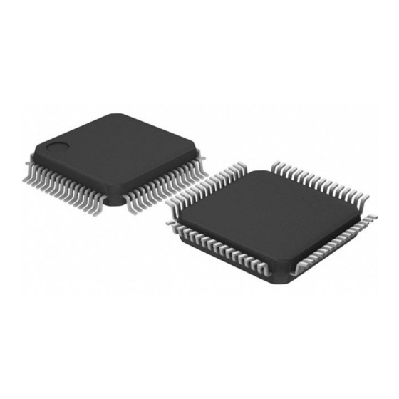
CS44600 10.PACKAGE DIMENSIONS 64L LQFP PACKAGE DRAWING Note: See Legend Below ∝ Figure 32. 64-Pin LQFP Package Drawing INCHES MILLIMETERS 0.55 0.063 1.40 1.60 0.002 0.004 0.006 0.05 0.10 0.15 0.007 0.008 0.011 0.17 0.20 0.27 0.461 0.472 BSC 0.484 11.70... -
Page 75: 11.Thermal Characteristics
Rail CS44600-DQZ fier Controller 6-Channel Digital Ampli- Tape and CS44600 LQFP -40° to +85° C CS44600-DQZR fier Controller Reel CS44600/800 Evalua- CDB44800 CDB44800 tion Board 8x50 W Half-Bridge CRD44800 CRD44800 Reference Design Board 8x60 W Full-Bridge CRD44800-ST-FB CRD44800-ST-FB Reference Design Board... - Page 76 OTHER AGENTS FROM ANY AND ALL LIABILITY, INCLUDING ATTORNEYS’ FEES AND COSTS, THAT MAY RESULT FROM OR ARISE IN CONNECTION WITH THESE USES. Cirrus Logic, Cirrus, the Cirrus Logic logo designs, and Popguard are trademarks of Cirrus Logic, Inc. All other brand and product names in this document may be trademarks or service marks of their respective owners.
Need help?
Do you have a question about the CS44600 and is the answer not in the manual?
Questions and answers