Table of Contents
Advertisement
Quick Links
User Manual
2ED4820-EM EB2 2HSV48
About this document
Scope and purpose
This document describes how to use the evaluation board 2ED4820-EM EB2 2HSV48.
Intended audience
Engineers who want to evaluate the capabilities of the 2ED4820-EM 48V high side gate driver in an easy and
flexible way, at medium current levels (up to 20A DC).
Table of contents
About this document ....................................................................................................................... 1
Table of contents ............................................................................................................................ 1
1
Introduction to the 2ED4820-EM EB2 2HSV48............................................................................. 2
1.1
Overview .................................................................................................................................................. 2
1.2
Key features ............................................................................................................................................. 4
1.2.1
Typical connection with a PC and a power supply (Common source + High side current sense) .. 4
1.3
Mandatory jumpers ................................................................................................................................. 5
1.4
Configuring the current sense position .................................................................................................. 5
1.4.1
Low side current sense:...................................................................................................................... 5
1.4.2
High side current sense: ..................................................................................................................... 6
1.5
Overview of the power configurations which can be tested ................................................................. 6
1.5.1
Common drain power configuration (1 single load): ........................................................................ 6
1.5.2
Common source power configuration, 1 single load: ....................................................................... 7
1.5.3
Common source power configuration, 2 loads: ................................................................................ 8
1.6
Level shifter and end-of-charge detector ............................................................................................. 10
2
Software user manual ............................................................................................................ 13
2.1
Prerequiresites ...................................................................................................................................... 13
2.1.1
Installing the Config Wizard for 2ED4820 EB ................................................................................... 13
2.1.2
Flashing the XMC2Go........................................................................................................................ 14
2.2
Accessing the user guide in the 'Help' menu ........................................................................................ 16
3
Board connectors description ................................................................................................. 17
3.1
Power connectors ................................................................................................................................. 17
3.2
Interface connectors ............................................................................................................................. 17
3.2.1
Connector J1 .................................................................................................................................... 17
3.2.2
Connector J2 .................................................................................................................................... 17
3.2.1
Connector J3 .................................................................................................................................... 18
3.3
Test points ............................................................................................................................................. 18
4
Schematic ............................................................................................................................ 19
5
Bill of Material ...................................................................................................................... 21
1
PCB: layers ........................................................................................................................... 23
Revision history ............................................................................................................................. 25
www.infineon.com
Please read the Important Notice and Warnings at the end of this document
page 1 of 26
1.0
2022-01-20
Advertisement
Table of Contents

Subscribe to Our Youtube Channel
Related Manuals for Infineon 2ED4820-EM EB2 2HSV48


Summary of Contents for Infineon 2ED4820-EM EB2 2HSV48
- Page 1 2ED4820-EM EB2 2HSV48 About this document Scope and purpose This document describes how to use the evaluation board 2ED4820-EM EB2 2HSV48. Intended audience Engineers who want to evaluate the capabilities of the 2ED4820-EM 48V high side gate driver in an easy and flexible way, at medium current levels (up to 20A DC).
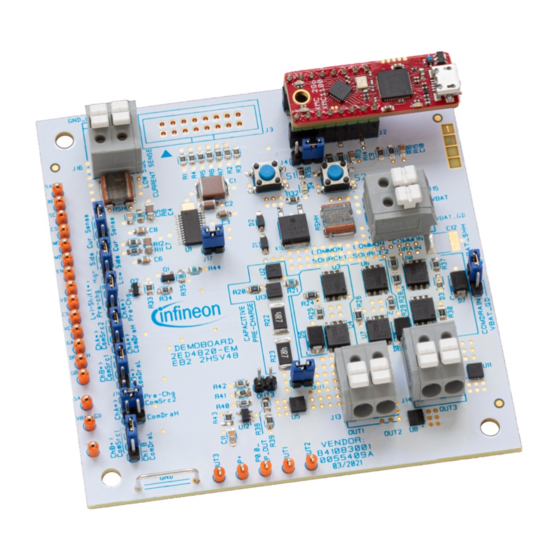
- Page 2 Introduction to the 2ED4820-EM EB2 2HSV48 Overview The 2ED4820-EM EB2 2HSV48 from Infineon Technologies is a flexible evaluation board designed to showcase the capabilities of the 2ED4820-EM. This board includes Infineon’s XMC1100 XMC2Go daughter board to interface to a PC over a USB cable.
- Page 3 2ED4820-EM EB2 2HSV48 Introduction to the 2ED4820-EM EB2 2HSV48 Figure 2 Power section overview User Manual www.infineon.com page 3 of 26 2022-01-20...
-
Page 4: Key Features
2ED4820-EM EB2 2HSV48 Introduction to the 2ED4820-EM EB2 2HSV48 Key features • The evaluation board is able to deliver a continuous DC current up to 20A per channel It comes with a jumper-based configurability, to test various topologies. Warning: make sure to completely configure the jumpers before turning ON the power supply!! - Page 5 2ED4820-EM EB2 2HSV48 Introduction to the 2ED4820-EM EB2 2HSV48 Mandatory jumpers The 2ED4820-EM EB2 2HSV48 comes with two jumpers: J4 for supply selection and J17 for GND connection. Both jumpers have to be kept on the board for proper operation: Figure 4 Mandatory jumpers.
- Page 6 2ED4820-EM EB2 2HSV48 Introduction to the 2ED4820-EM EB2 2HSV48 1.4.2 High side current sense: This configuration is used to sense the current thanks to a low ohmic shunt connected to the supply node: Figure 6 Configuration for low side current sense.
- Page 7 2ED4820-EM EB2 2HSV48 Introduction to the 2ED4820-EM EB2 2HSV48 Figure 8 Configuring the jumpers & connecting the load. 1.5.2 Common source power configuration, 1 single load: Channel A drives the ohmic path to pre-charge capacitor(s), connected thanks to a jumper on J7 •...
- Page 8 2ED4820-EM EB2 2HSV48 Introduction to the 2ED4820-EM EB2 2HSV48 Figure 10 Configuring the jumpers & connecting the load. 1.5.3 Common source power configuration, 2 loads: Channel A drives the low-ohmic path on OUT2 • Channel B drives the low-ohmic path on OUT1 •...
- Page 9 2ED4820-EM EB2 2HSV48 Introduction to the 2ED4820-EM EB2 2HSV48 Figure 12 Configuring the jumpers & connecting the load. User Manual www.infineon.com page 9 of 26 2022-01-20...
- Page 10 2ED4820-EM EB2 2HSV48 Introduction to the 2ED4820-EM EB2 2HSV48 Level shifter and end-of-charge detector The 2ED4820-EM 2HSV48 EB comes with two features external to 2ED4820-EM: 1. High voltage level shifter, to optionally drive the resistive path for capacitor pre-charge either from an MCU GPIO (P0.14_LSh) or from an external waveform generator (using TP23)
- Page 11 2ED4820-EM EB2 2HSV48 Table of contents Figure 14 End of charge detector. The voltage out of the resistive path, which is charging the capacitor, is compared to a reference voltage generated from the supply voltage supplying the board. R38 & R39 divide the voltage on the capacitor: CP+ is biased to 12/(270+12) = 4.255 % of OUT1 voltage.
- Page 12 2ED4820-EM EB2 2HSV48 Table of contents Figure 15 End of charge detector: scope capture. User Manual www.infineon.com page 12 of 26 2022-01-20...
- Page 13 XMC2Go daughter board by sending/receiving messages over USB: Config Wizard for 2ED4820 EB. Prerequiresites 2.1.1 Installing the Config Wizard for 2ED4820 EB For your PC to interact with the XMC2Go over USB, install the Infineon Developer Center launcher from this link: Infineon Developer Center Launcher, using a web browser: Figure 16 Installing the Infineon Developper Center.
- Page 14 PC thanks to a micro USB cable. To ensure consistency with the Config Wizard for 2ED4820 EB software running on the PC, it is necessary to flash the firmware of the XMC microcontroller. step: launch the Config Wizard for 2ED4820 EB software on the PC, from the Infineon Developer Center: Figure 18 Launching the program.
- Page 15 2ED4820-EM EB2 2HSV48 Table of contents step: establish the connection with the XMC2Go board: Figure 20 Selecting the Com Port & activating the connection. step: flash the firmware in the XMC MCU memory Figure 21 Flash the XMC MCU code.
- Page 16 2ED4820-EM EB2 2HSV48 Table of contents Accessing the user guide in the ‘Help’ menu Access the help menu to discover the functionality of the Config Wizard for 2ED4820 EB software (the help opens in a web browser, as an html file): Figure 22 On-line user guide.
-
Page 17: Power Connectors
2ED4820-EM EB2 2HSV48 Table of contents Board connectors description Power connectors Name Connector Type Description VBAT J15/1 Power supply Positive power supply 48V J16/2 Ground power Ground GND_Load J16/1 Ground power Ground connection for the load, in low side current sense configuration... -
Page 18: Test Points
2ED4820-EM EB2 2HSV48 Table of contents 3.2.1 Connector J3 Note: J3 is not assembled, reference = 09195166324 from Harting or compatible connector Name Type Description No connected Ground Ground No connected P0.14_LSh Supply 5V supply, connects to VDD pin of 2ED4820-EM if a jumper is positioned on pins 2 &... - Page 19 2ED4820-EM EB2 2HSV48 Table of contents Schematic Figure 23 Schematic: power section User Manual www.infineon.com page 19 of 26 2022-01-20...
- Page 20 2ED4820-EM EB2 2HSV48 Table of contents Figure 24 Schematic: gate driver section User Manual www.infineon.com page 20 of 26 2022-01-20...
-
Page 21: Bill Of Material
2ED4820-EM EB2 2HSV48 Table of contents Bill of Material Item Identifier Value Charact. Footprint 4.7µF 100V/X7R 2220 2.2µF 25V/X7R 1206 220nF 100V/X7R C4, C7 1µF 16V/X7R 1206 C5, C9, C10, C11 100nF 16V/X7R C6, C8 100p 16V/X7R 2220 MMSZ5256BT1G Zener 30V... - Page 22 2ED4820-EM EB2 2HSV48 Table of contents TP17, TP18, TP19, TP20, TP21, TP22, TP23 2ED4820-EM SPI gate TSDSO24 driver U2, U5, U8, U11, U13 IAUZ40N08S5N100 10mΩ NMOS S3O8 U3, U4, U6, U7, U9, U10 IAUC100N08S5N043 4.3mΩ NMOS SSO8 IPD50N10S3L-16 15mΩ NMOS...
-
Page 23: Pcb: Layers
2ED4820-EM EB2 2HSV48 Table of contents PCB: layers Figure 25 Top and bottom layers Figure 26 Inner planes User Manual www.infineon.com page 23 of 26 2022-01-20... - Page 24 2ED4820-EM EB2 2HSV48 Table of contents Figure 27 Top assembly User Manual www.infineon.com page 24 of 26 2022-01-20...
-
Page 25: Revision History
2ED4820-EM EB2 2HSV48 Revision history Revision history Document Date of release Description of changes version Rev 1.0 2022-01-20 Initial version User Manual www.infineon.com page 25 of 26 2022-01-20... - Page 26 (“Beschaffenheitsgarantie”) . dangerous substances. For information on the types With respect to any examples, hints or any typical Infineon Technologies AG in question please contact your nearest Infineon values stated herein and/or any information Technologies office. 81726 Munich, Germany...
Need help?
Do you have a question about the 2ED4820-EM EB2 2HSV48 and is the answer not in the manual?
Questions and answers