
Related Manuals for CIS VCC-5CL1R


Summary of Contents for CIS VCC-5CL1R
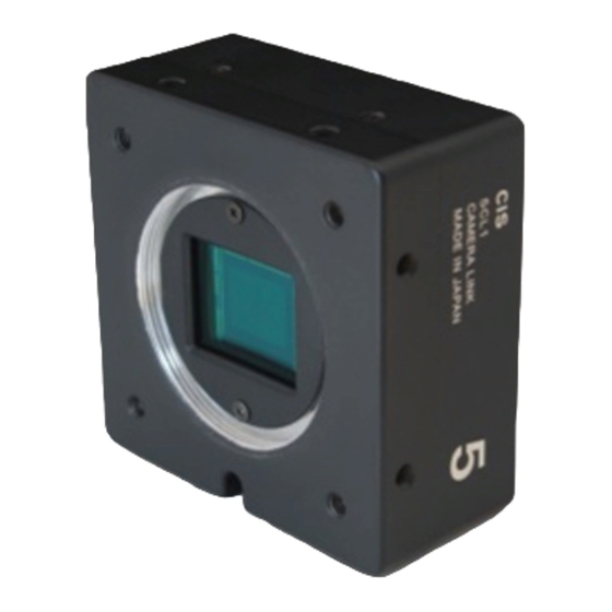
- Page 1 VCC-5CL1R Rev. 905-0022-02 English Camera Link I/F 5.2M Pixels CMOS Color (RAW) Camera VCC-5CL1R Product Specifications & Operational Manual CIS Corporation ©2015 CIS Corporation. All rights reserved.
-
Page 2: Table Of Contents
CC mode ..............................32 13.3. Precaution and Instruction ........................33 Factory Settings ..............................34 CMOS Optical Axis Accuracy ..........................35 Dimensions ................................. 36 Cases for Indemnity (Limited Warranty) ........................ 37 CMOS Pixel Defect ............................... 37 ©2015 CIS Corporation. All rights reserved. - Page 3 VCC-5CL1R Rev. 905-0022-02 Product Support ..............................37 Ordering Information ............................37 μT-License ................................37 ©2015 CIS Corporation. All rights reserved.
-
Page 4: Scope Of Application
VCC-5CL1R Rev. 905-0022-02 Scope of Application This is to describe VCC-5CL1R, 1-inch type CMOS, 5.2M resolution, Camera Link Color (RAW) Camera. All specifications contained herein are subject to change without prior notice. Reproduction in whole or in part is prohibited. -
Page 5: Product Outline
VCC-5CL1R Rev. 905-0022-02 3. Product Outline VCC-5CL1R is a Camera Link interfaced, 1-inch type CMOS, 5.2M resolution industrial Color camera. Entire pixels can be read out within 1/59s at Medium Configuration output Features Global shutter CMOS sensor. □ Camera Link Base, Medium, Full, and Deca configuration are supported. -
Page 6: Specification
Refer to drawing for CMOS Optical Axis Accuracy. (16) Gain variable range 0dB ~ +18dB (17) Shutter speed variable range OFF ~ 1/99000s (at 10Tap Configuration) (18) Trigger shutter mode Fixed Shutter Trigger Mode/ Pulse Width Shutter Trigger Mode ©2015 CIS Corporation. All rights reserved. - Page 7 Camera operation guaranteed temperature: -5℃ ~ +45℃ with no condensation ※All the camera functions operate normally under operation guaranteed temperature. RH 20~80% with no condensation. Humidity (24) Storage Environment -25℃ ~ +60℃ Temperature RH 20~80% with no condensation. Humidity ©2015 CIS Corporation. All rights reserved.
-
Page 8: Camera Input/Output Signals Specification
White Clip Level At Digital 8bit : FFh Setup Level At Digital 8bit : 01±01h (Condition: Gain 0dB) Dark Shading At Digital 8bit : Both horizontal and vertical should be under 04h. (Condition: Gain 0dB) ©2015 CIS Corporation. All rights reserved. - Page 9 ・At high level, regardless of input voltage, the photo coupler operates with 4mA current circuit and drive. ・The delay time of the photo coupler input/output transmission is approx. 5μs with t_on, and 35μs with t_off 6 pin 10 pin TLP291SE (Toshiba) ©2015 CIS Corporation. All rights reserved.
- Page 10 ・Please refer to the Table below for the output voltage with the combination of pull up voltage and pull up register Pull up voltage(V) at the user side Pull up resistor(Ω) Output voltage(V) 4.7k 4.7k 2.7k 1.2k ©2015 CIS Corporation. All rights reserved.
-
Page 11: Spectral Response
Bayer Pattern will also be reversed if horizontal flip function for the output images is set to "flip ※ horizontal." (1) 2Tap Base Configuration Mode : 30fps Full Frame 2560pixel ・・・ (2) 4Tap Medium Configuration Mode : 59fps Full Frame (Factory setting) 2560pixel ・・・ ©2015 CIS Corporation. All rights reserved. - Page 12 VCC-5CL1R Rev. 905-0022-02 (3) 8Tap Full, 8Tap 10bit Configuration Mode : 117fps Full Frame 2560pixel ・・・ (4) 10Tap 8bit Configuration Mode : 140fps Full Frame 2560pixel ・・・ 9 10 ©2015 CIS Corporation. All rights reserved.
-
Page 13: Camera Function Settings
Manual Gain (refer to Address 21) Manual Gain 0 ~ 768: 0 ~ +18dB (1dig=0.0234375dB) 0 ~ 15: Preset Shutter * Refer to the Section 5.2 Table for Preset Shutter Value Shutter Manual Shutter (refer to the Address 24) ©2015 CIS Corporation. All rights reserved. - Page 14 Sequence Parameter Set 7 6 Params Manual Calibration RECAL None Execute sensor calibration manually. Initial Setting INIT None Set the settings back to the initial settings. Data Save SAVE None Save the camera settings. ©2015 CIS Corporation. All rights reserved.
-
Page 15: Note For Functions
1/1000 1/1000 1/2000 1/2000 1/2000 1/2000 1/2500 1/2500 1/2500 1/2500 1/5000 1/5000 1/5000 1/5000 1/11000 1/10000 1/10000 1/10000 1/14000 1/16000 1/16000 1/15000 1/26000 1/26000 1/25000 1/24000 1/44000 1/44000 1/53000 1/49000 1/44000 1/68000 1/93000 1/99000 ©2015 CIS Corporation. All rights reserved. - Page 16 1/1300 1/1300 1/2700 1/2600 1/2700 1/2700 1/3400 1/3300 1/3300 1/3300 1/6600 1/6500 1/6700 1/6600 1/15000 1/14000 1/13000 1/14000 1/18000 1/20000 1/20000 1/20000 1/32000 1/32000 1/32000 1/31000 1/53000 1/53000 1/63000 1/59000 1/53000 1/78000 1/103000 1/108000 ©2015 CIS Corporation. All rights reserved.
-
Page 17: Calculation Of Exposure Time
External Connector Pin Assignment 6.1. 12 pins Circular Connector HR10-10R-12PA (HIROSE) equivalent Pin No. Signals Power Input (DC+10.8V~25V) TRIGGER Input +(isolated) EXPOSURE/FVAL Output +(isolated) EXPOSURE/FVAL Output (TTL) TRIGGER Input −(isolated) TRIGGER Input (TTL) EXPOSURE/FVAL Output −(isolated) ©2015 CIS Corporation. All rights reserved. -
Page 18: Camera Link Connector 12226-1100-00Pl (Sumitomo 3M)
Blinking :Power supply via only CL1 cable or via only CL2 cable Lighting : Power supply via both CL1 cable and CL2 cable *Since the required current exceeds the tolerable range of one PoCL cable, please make sure to supply power via two cables. ©2015 CIS Corporation. All rights reserved. -
Page 19: Timing Diagram
LVAL of FVAL outputs Lo for approx. 1H at start-up. □ The delay time between the completion of exposure (The down edge of exposure time) to the start-up of □ FVAL includes uncertain delay time less than 1H. ©2015 CIS Corporation. All rights reserved. -
Page 20: Horizontal Synchronous Signals Timing (4Tap Medium Configuration Mode: 59Fps) *Factory Setting
LVAL of FVAL outputs Lo for approx. 1H at start-up. □ The delay time between the completion of exposure (The down edge of exposure time) to the start-up of □ FVAL includes uncertain delay time less than 1H. ©2015 CIS Corporation. All rights reserved. -
Page 21: Horizontal Synchronous Signals Timing (8Tap Full, 8Tap 10Bit Configuration Mode: 117Fps)
DVAL is not output at 8Tap 10 bit mode. SP Out is not output either. (Exposure Out can be output only via □ 12pin circular connector). The delay time between the completion of exposure (The down edge of exposure time) to the start-up of □ FVAL includes uncertain delay time less than 1H. ©2015 CIS Corporation. All rights reserved. -
Page 22: Horizontal Synchronous Signals Timing (10Tap 8Bit Configuration Mode: 140Fps)
LVAL of FVAL outputs Lo for approx. 1H at start-up. □ The delay time between the completion of exposure (The down edge of exposure time) to the start-up of □ FVAL includes uncertain delay time less than 1H. ©2015 CIS Corporation. All rights reserved. -
Page 23: Fixed Trigger Shutter Mode
Effective Line Invalid Video Out Line Exposure Time LVAL Out DVAL Out FVAL Out Exposure Time Delay Effective Line : 2048H Trigger input ignore period TRIG IN SP Out Exposure time delay (Exposure Out) ©2015 CIS Corporation. All rights reserved. -
Page 24: Pulse Width Trigger Shutter Mode
Any trigger input between Exposure Time start and Read-out start shall be ignored in the camera as □ shown (A) below. When a read-out period (FVAL=1) and the exposure start (start-up of Exposure Time) are overlapped, LVAL and DVAL output Low for 4H, and stop outputting images. ©2015 CIS Corporation. All rights reserved. -
Page 25: Shading Correction
Shoot a uniform object such as a pattern box, to full screen, then turn shading detection ON (address 44), to calculate and save the correction data automatically in the camera. *When setting a shading correction data, please make sure that Horizontal Partial Mode, Vertical Partial Mode, and Binning Mode are OFF. ©2015 CIS Corporation. All rights reserved. -
Page 26: Vertical Partial Scan Mode
51 and 52. Either method provides the same operation. However, please be noted that the above settings are reflected only when “1” is written in the address 54. Write “0” in the address 54 to set vertical partial setting OFF. □ ©2015 CIS Corporation. All rights reserved. -
Page 27: Horizontal Partial Mode (Selection Of Horizontal Pixel Number)
10Tap mode 2560pixel × 2048Line 29.9 fps 59.4 fps 116.9 fps 140.3 fps 2048pixel × 2048Line 37.1 fps 74.2 fps 148.4 fps 175.4 fps 1920pixel × 2048Line 39.8 fps 78.8 fps 156.5 fps 186.7 fps ©2015 CIS Corporation. All rights reserved. -
Page 28: Binning Mode
2Tap mode 4Tap mode 8Tap mode 10Tap mode 2×2 binning (1280pixels × 1024lines) 59.1 fps 177.3 fps 231.1 fps 277.3 fps 4×4 binning (640pixels × 512lines) 115.5 fps 229.2 fps 451.5 fps 541.7 fps ©2015 CIS Corporation. All rights reserved. -
Page 29: Serial Communication Function
[¥r] [¥n] [Linefeed] [sp]=Space(0x20) [Returned value] >[sp] [Prompt + Space] 【Example for Set Command】 To set 30 to the address 10 [Send] SU[sp]10[sp]30[¥r]or[¥n] [Returned value] [¥r] [¥n] [Linefeed] [Returned value] >[sp] [Prompt + Space] ©2015 CIS Corporation. All rights reserved. - Page 30 Input “INIT” to return to the factory settings. (Data are not saved at this point.) Data Save Input “SAVE” to save the camera settings. [Returned value] [¥r] [¥n] [Linefeed] [Returned value] >[sp] [Prompt + Space] ©2015 CIS Corporation. All rights reserved.
-
Page 31: Sequence Control Function
The limitation of the trigger input timing at Sequence Control is the same as the one at Normal Mode. (Refer to the Section 7.9 and Section 7.10.) The signal level of CC2~4 signals have to be stable by the time of trigger input. (setup time = 50[ns]) ©2015 CIS Corporation. All rights reserved. -
Page 32: Auto Mode
Auto Mode Flow Chart Sequence Index (Address 73) Link each Index and the parameter sets. Sequence Index repeat (Address 74) Sequence Index range (Address 72) Repeating counts of each Index Range of Index to execute ©2015 CIS Corporation. All rights reserved. -
Page 33: Cc Mode
This is a mode to specify the Index number directly with CC2, CC3, and CC4 signals. Whenever a trigger is input, the Index specified by the CC signal is selected and the corresponding parameter set values are applied to the camera. CC Mode Flow Chart Sequence Index (Address 73) Link each Index and the parameter sets. Input Output Index No. ©2015 CIS Corporation. All rights reserved. -
Page 34: Precaution And Instruction
6033 6612 Unit: fps Effective Line (Exposure Line Count) Unit: line Total Line Number Unit: line Horizontal 1920 Pixels Cycle 400.13 238.88 157.23 147.23 Unit: µs Frame Rate 2499 4186 6360 6792 Unit: fps ©2015 CIS Corporation. All rights reserved. -
Page 35: Factory Settings
200: 200[%] Gamma Correction Shading Correction Vertical Partial Mode OFF (2048 lines) Horizontal Partial Mode 2560 pixels (Selection of Horizontal Pixel Number) Binning Mode Sequence Control (ON/OFF) PoCL side Power Supply Switch at rear ©2015 CIS Corporation. All rights reserved. -
Page 36: Cmos Optical Axis Accuracy
VCC-5CL1R Rev. 905-0022-02 CMOS Optical Axis Accuracy ©2015 CIS Corporation. All rights reserved. -
Page 37: Dimensions
VCC-5CL1R Rev. 905-0022-02 Dimensions ©2015 CIS Corporation. All rights reserved. -
Page 38: Cases For Indemnity (Limited Warranty)
CMOS pixel defects might be noted with time of usage of the products. Cause of the CMOS pixel defects is the characteristic phenomenon of CMOS itself and CIS is exempted from taking any responsibilities for them. Should you have any questions on CMOS pixel defects correction, please contact us.
Need help?
Do you have a question about the VCC-5CL1R and is the answer not in the manual?
Questions and answers