
Related Manuals for CIS VISION:mini VCC-GC20V41CL


Summary of Contents for CIS VISION:mini VCC-GC20V41CL
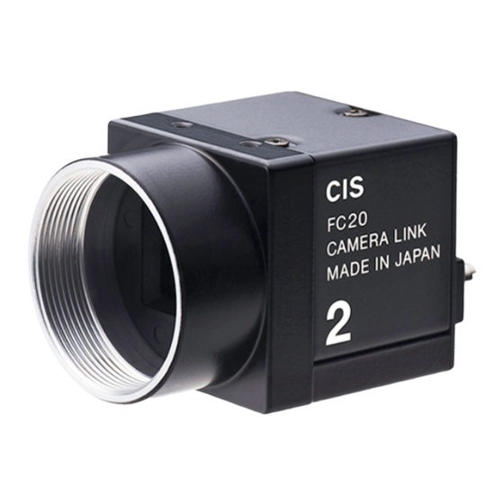
- Page 1 VCC-GC20V41CL Rev.900-721-32-00 English 29mm cubic VGA High-Speed B/W CMOS Camera VCC-GC20V41CL Product Specification & Operational Manual CIS Corporation ©2011 CIS Corporation. All rights reserved.
-
Page 2: Table Of Contents
Remote Interface Function ........................... 18 Initial Settings ..............................19 CMOS Optical Axis Accuracy ..........................20 Dimensions ................................. 21 Cases for Indemnity (Limited Warranty) ........................ 22 Sensor Pixel Defect .............................. 22 Product Support ..............................22 ©2011 CIS Corporation. All rights reserved. -
Page 3: Scope Of Application
AC leaks from the connected devices may cause damages or destroy the camera. Do not apply excessive voltage. (Use only the specified voltage.) Unstable or improper power supply voltage may cause damages or malfunction of the camera. ©2011 CIS Corporation. All rights reserved. - Page 4 The rising time of camera power supply voltage shall be less than +10V, Max 60ms. Please avoid noises like chattering when rising. Voltage Rising Time [ ms ] In case of abnormal operation, contact the distributor from whom you purchased the product. ©2011 CIS Corporation. All rights reserved.
-
Page 5: Notes On Partial Scan Mode Operation
□ Shutter Speed: 1/500s ~1/50,000s □ Fixed Trigger Shutter Mode □ Pulse Width Trigger Shutter Mode □ Partial Scan Mode (Vertical) □ Free sample control software for evaluation purpose only is downloadable via our web. ©2011 CIS Corporation. All rights reserved. -
Page 6: Specification
(17) Gamma 1(Fixed) (18) Shutter speed OFF(1/500),1/750s,1/1000s,1/1500s,1/2000s,1/2500s,1/4000s,1/5000s,1/10000s,1/15000s, variable range 1/20000s,1/25000s,1/30000s,1/40000s,1/50000s ・Fixed Trigger Shutter Mode (19) Trigger shutter mode ・Pulse Width Trigger Shutter Mode (Exposure time is set with the pulse width of trigger signal.) ©2011 CIS Corporation. All rights reserved. - Page 7 (100G) for ±X, ±Y, and ±Z, 6 Shock directions. (without package) Operation guaranteed: -5℃~+45℃ Temperature Performance guaranteed: 0℃~+40℃ (22) Operation environment Humidity RH 20~80% with no condensation -25℃ ~ +60℃ Temperature (23) Storage environment RH 20~80% with no condensation Humidity ©2011 CIS Corporation. All rights reserved.
-
Page 8: Camera Output Signal Specification
100Ω VD,HD HD74LV1GT32ACME Exposure Output (RENESAS) 47pF Voh 3.8V (Min) Vol 0.55V (Max) 100Ω Trigger Input HD74LV1GT14 ACME (RENESAS) 1KΩ 470pF Vih 2.0V (Min) Vil 0.8V (Max) 6pins Circular Connector at rear: GPIO interface ©2011 CIS Corporation. All rights reserved. -
Page 9: Cmos Spectral Response (Representative Value)
VCC-GC20V41CL Rev.900-721-32-00 CMOS Spectral Response (Representative value) 5.3. ※Lens characteristics and illuminant characteristics are not considered. Video Output Format 5.4. VGA 500fps Mode: 2Tap Interleaved DA DB DA DB From Camera (2 Tap Output) ©2011 CIS Corporation. All rights reserved. -
Page 10: Camera Link Port Data Bit Assignment (Base Configuration)
Not in use DB:bit2 Port C3 Not in use DB:bit3 Port C4 Not in use DB:bit4 Port C5 Not in use DB:bit5 Port C6 Not in use DB:bit6 Port C7 Not in use DB:bit7 ©2011 CIS Corporation. All rights reserved. -
Page 11: Function Settings
1line Time [s] = ((output pixels/2tap)+5)×1/79.99MHz Manual Shutter Control 009&010 At full frame scan, output pixels = 480 1line Time ≒ 4.06μs ※Address 002 data shall be 016. Address 009 MSB and Address 010 LSB make 11bit in total. ©2011 CIS Corporation. All rights reserved. - Page 12 Address 019 MSB and Address 020 LSB make 11bit in total. ※Address 005 data shalla be 002. 9600bps 19200bps Remote Communication 38400bps Baud Rate Setting 57600bps 115200bps 5~255: 9600bps Input 083 to save address 000 ~ 031 to EEP-ROM. Data Save ©2011 CIS Corporation. All rights reserved.
-
Page 13: External Connector Pin Assignment
Trigger IN(TTL level) Exposure 26pins Mini Camera Link Connector 12226-1100-00 PL (SUMITOMO 3M) 7.2. Pin No. Pin No. Xclk- Xclk+ SerTC+ SerTC- SerTFG- SerTFG+ CC1- (Trigger IN-) CC1+ (Trigger IN+) CC2+ CC2- CC3- CC3+ CC4+ CC4- ©2011 CIS Corporation. All rights reserved. -
Page 14: Timing Chart
LVAL Output · · · · · · · 479 480 DVAL Output · · · · · · · FVAL Output 10 H 480 H ※Video output signal delays by 2H from Exposure Time. ©2011 CIS Corporation. All rights reserved. -
Page 15: Fixed Trigger Shutter Mode
479 480 DVAL Output ・ ・ ・ ・ ・ FVAL Output 480 H 10 H Trigger Input Exposure Time Exposure Time Delay(Fixed) (nHD ×4.06μs ) 330ns ※Video output signal delays by 2H from Exposure Time. ©2011 CIS Corporation. All rights reserved. -
Page 16: Pulse Width Trigger Shutter Mode
479 480 DVAL Output ・ ・ ・ ・ ・ FVAL Output 480 H 10 H Trigger Input Delay(Fixed) Delay(Fixed) 330ns 270ns Exposure Time Exposure Time ※Video output signal delays by 2H from Exposure Time. ©2011 CIS Corporation. All rights reserved. -
Page 17: Partial Scan Mode
The set manual shutter lines ≦ Vertical partial scan output lines If the condition above is not met, shutter lines to be set will be the same number as vertical partial scan output lines. ©2011 CIS Corporation. All rights reserved. -
Page 18: Remote Interface Function
Note: Once the data was saved into EEPROM, it may not be reset to t he initial settings. C is the code to send the data back from the camera. Note: Do not set code C when sending the data from PC side. ©2011 CIS Corporation. All rights reserved. -
Page 19: Initial Settings
Manual Gain Control 0: 0dB Manual Shutter Control 009&010 480: 1/500s Trigger Polarity 0: Positive Input Input Trigger Port Selection 0: Camera Link connector (12226-1100-00 PL) Output Data Selection 0: 8bit Output Data Baud Rate 0:9600bps ©2011 CIS Corporation. All rights reserved. -
Page 20: Cmos Optical Axis Accuracy
Inclination of effective pixels, Theta,?, to datum plane shall be ?? ±0.5° The center of effective pixels shall be within f 0.6 to the center of C lens mount (*) Dimensions from datum plane to the center of the lens mount 910-006-01-01 (Unit:mm) ©2011 CIS Corporation. All rights reserved. -
Page 21: Dimensions
Product Label Position (M2 size) *2)C mount screws comply with ANSI/ASME B1.1, 1-32UN(2B). *1)Screw length from the lens mount surface shall be under 6mm. And protruding portion shall be less than 10mm. 999-547-00-00 (Unit:mm) ©2011 CIS Corporation. All rights reserved. -
Page 22: Cases For Indemnity (Limited Warranty)
Sensor Pixel Defect Sensor pixel defects might be noted with time of usage of the products. Cause of the Sensor pixel defects is the characteristic phenomenon of CMOS itself and CIS is exempted from taking any responsibilities for them. Product Support When defects or malfunction of our products occur, and if you would like us to investigate on the cause and repair, please contact your distributors you purchased from to consult and coordinate.
Need help?
Do you have a question about the VISION:mini VCC-GC20V41CL and is the answer not in the manual?
Questions and answers